1. Introduction
Benefit from the excellent material properties of third-generation wide bandgap semiconductors, including large critical breakdown fields and low on-resistance. Gallium nitride (GaN) devices can provide higher drain-source voltage (
Uds) and much lower on-resistance (
Rdson) than traditional silicon devices. From the system level, gallium nitride devices can achieve low on-off loss and switching loss, as well as better system efficiency and power density by virtue of their excellent switching performance and high frequency operation capability. Therefore, it has a wide range of application prospects [
1]. At present, GaN power devices are predominantly applied in DC/DC converters [
2,
3]. For instance, the authors of [
4] presented a power supply prototype based on an active-clamp forward converter that utilizes GaN devices as the primary-side main switches, which feature a low gate charge, a low output capacitance, and zero reverse recovery loss, achieving a high efficiency and power density. While some applications extend to inverters, the majority remain in single-phase configurations [
5]. A representative case is presented in [
6], in which a comparative study was conducted on single-phase inverters employing silicon (Si), silicon carbide (SiC), and gallium nitride (GaN) power devices. However, the application of GaN in three-phase inverters remains largely unexplored in the current literature.
Table 1 compares the typical parameters of three mass-produced switching transistors currently available on the market. As can be seen from the table, under the same rated voltage and current specifications, GaN power devices exhibit lower on-resistance compared to the other two silicon-based devices, translating to lower conduction losses and higher efficiency. The gate charge (Qg) of this model of GaN power device is only 2.2 nC. This indicates that GaN devices require less charge to be transferred during switching transitions. Such characteristics demonstrate GaN power devices’ capability to complete state transitions (off-to-on or on-to-off) within shorter time windows, thereby enabling higher switching frequencies. The switching delay parameters in
Table 1 reveal that the turn-on delay (
td_on) of Si-based power devices is nearly 3 times longer than GaN-based counterparts, while the turn-off delay (
td_off) shows an even greater disparity of 5 to 8 times. Furthermore, GaN devices exhibit significantly lower input capacitance (
Ciss) compared to silicon solutions—a critical advantage for high-frequency applications. The reduced
Ciss not only minimizes driver current requirements but also simplifies gate drive circuitry design and decreases associated switching losses.
Anticipated comparative analysis reveals that GaN-based three-phase inverters demonstrate superior switching frequencies, reduced power losses, enhanced energy conversion efficiency, and more compact form factors compared to their traditional Si-based counterparts.
Consequently, implementing GaN power devices in three-phase inverters to achieve high-frequency operation and system miniaturization carries substantial technical significance. However, next-generation converters characterized by high-frequency operation, high efficiency, and a high-power density impose more stringent requirements on system control strategies.
Researchers have made substantial improvements and innovations to existing control strategies targeting diverse challenges [
7,
8]. Notably, the authors of [
9] proposed a novel control design method based on the off-policy IRL method, presented to deal with the problem of the TTP grid-connected power quality degradation caused by uncertain parameters under grid voltage disturbance. Other researchers proposed a new dual-mode robust model predictive control (RMPC) strategy, which is suitable for three-phase inverters with LCL filters in two operating modes, GC (grid-connected), and SA (off-grid), under the condition of uncertain filter parameters [
10]. Reference [
11] addressed unbalanced loads by proposing a separate sequential control strategy, which enables rapid restoration to target values during load transients and enhances voltage stability. Although numerous studies have been conducted on three-phase inverter composite control strategies, they are predominantly based on IGBT-based three-phase inverter topologies [
12,
13]. Moreover, most of these control strategy studies are based on the switching frequency of 0~20 kHz, which cannot guarantee the control effect under >100 kHz.
The implementation of GaN devices in high-frequency three-phase inverters necessitates stringent control methodologies, primarily due to their ultra-fast switching speeds (ns-range), steep voltage/current transients, dead-time sensitivity, and the inherent challenge of balancing low on-resistance with switching losses. Furthermore, parasitic elements (e.g., inductances/capacitances) exhibit amplified effects at elevated frequencies, requiring system dynamics to achieve enhanced responsiveness—exemplified by microsecond-level adjustments during load transients. Conventional control schemes (e.g., PI-based approaches) struggle to reconcile bandwidth requirements with robustness, thereby necessitating advanced control architectures featuring the following:
Strong disturbance rejection;
Adaptive modulation schemes;
Real-time parameter optimization.
Such methodologies are critical to fully exploit GaN’s high-frequency potential while ensuring operational stability.
Therefore, to address the high-frequency control requirements of GaN-based three-phase inverters, a linear active disturbance rejection control (LADRC) strategy is introduced. After performing PARK transformation on the three-phase voltages, predictive tracking of the transformed dq-axis voltages is achieved through a linear extended state observer (LESO). A simulation model is developed using Simulink (R2023a); the digital control algorithm design is completed based on DSP28034. Finally, a 500 W three-phase digital inverter prototype is constructed. The prototype has the following features:
- (1)
The main topology employs GaN power devices for all switching components;
- (2)
Digital control implementation is achieved using DSP28034, with space vector pulse width modulation (SVPWM) as the modulation scheme;
- (3)
The output stage adopts LCL filtering, significantly reducing the output capacitance value.
3. Key Parameter Design
The prototype design indicators are as follows:
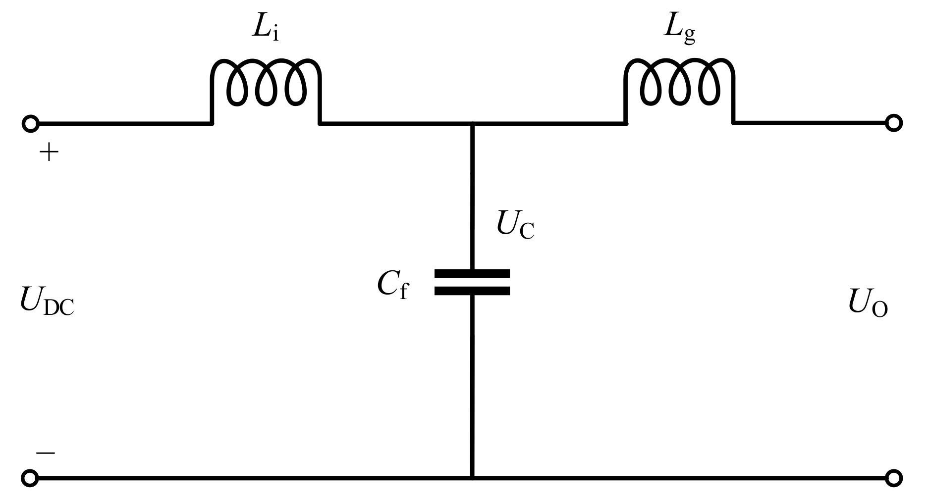
The output filter adopts the LCL structure. Taking phase A as an example, the specific parameter calculation process is as follows:
First, LCL is equivalent to a single phase as shown in
Figure 2 below:
According to the inductance current Δ
I1 formula, the following can be observed:
where
UDC is the filter capacitor voltage,
Ton is the inductor,
Li, current rise time and the switching tube opening time. Under SVPWM, this is a quantity that varies with the sine function, then we can see the following:
where
m is the modulation coefficient,
Tsw = 1/
fSW, and can be obtained by synthesizing the above formula:
Considering only the resistive load, the filter capacitance voltage,
UC, is approximately equal to the fundamental component of the output voltage,
UDC, of the bridge arm. So
Since the maximum value of Δ
I1 occurs at sin
ωt = 1/2,
m = 311/350 ≈ 0.89. Current ripple rate
r = Δ
I1/
I, substituting the inductance,
Li, can be calculated as follows:
where
I =
Iga_max indicates the peak output current. Generally, the rated inductance current needs to be 1.2 to 1.5 times higher than the maximum load current to avoid core saturation. Considering the sufficient margin,
I = 2A, and the current ripple rate
r = 40%. By substituting these data,
Li ≥ 437.5 µH is calculated.
By using the formula,
the filter capacitor,
Cf, value is calculated, where
X is the total reactive power absorbed by the capacitor and
X = 3.5%.
Q is the rated power of phase A,
F = 50 Hz is the output frequency, and
Ug_max is the peak value of the output voltage
Uo;
Cf ≈ 1.15 µF is calculated by substituting these data. Considering the actual filtering effect, the selection of capacitance value should usually be greater than the theoretical calculation value, that is,
Cf ≥ 1.15 µF.
The ratio between two inductors is defined as
R, i.e.,
Lg =
RLi, and it is calculated using the following formula:
where
Iat denotes the ripple attenuation coefficient between inductors
Li and
Lg, defined as 10%. Substituting the data yields
R ≈ 1.13%, enabling the calculation of
Lg ≈ 4.94 µH. Due to the tolerance of the actual value of the inductance (usually ±10%), if the nominal value of 5 µH inductance is selected, the actual value may be 4.5–5.5 µH. The minimum 4.5 µH May not meet the attenuation demand. After 7 µH is selected, the actual inductance value ranges from 6.3 to 7.7 µH, and the minimum 6.3 µH is still higher than the calculated value, ensuring the lower limit of attenuation performance. Therefore, to ensure normal attenuation, a larger nominal inductance value of
Lg = 7 µH is ultimately selected.
4. Scheme Design
4.1. Control Scheme
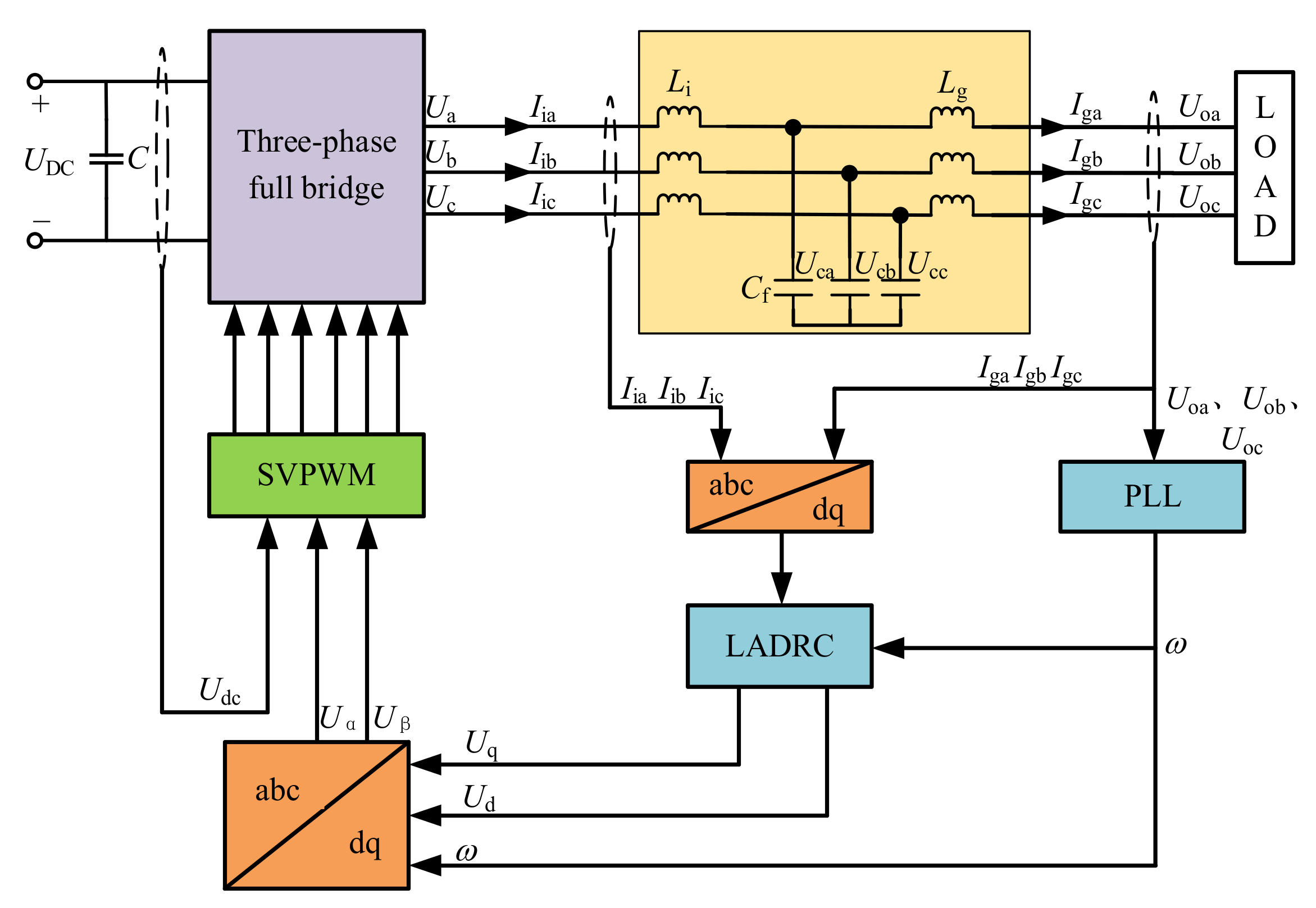
The core advantages of Linear Active Disturbance Rejection Control (LADRC) lie in its strong disturbance rejection capability and model adaptability. By utilizing a Linear Extended State Observer (LESO), it can estimate and compensate for both internal and external system disturbances in real-time. This significantly reduces the dependence on precise mathematical models. Additionally, its simple linear structure facilitates engineering implementation. Compared to traditional PID control, this method improves dynamic response speed and robustness, making it particularly suitable for high-frequency, high-interference operating conditions in GaN inverters. Moreover, the parameter tuning of LADRC is intuitive, effectively balancing disturbance rejection performance and stability. It compensates for the shortcomings of traditional control methods in suppressing broadband interference. So, the system employs a linear active disturbance rejection control (LADRC) strategy, and a control block diagram is depicted in
Figure 3. The three-phase full-bridge configuration utilizes space vector pulse width modulation (SVPWM). The sample signals include the following:
Simultaneously, the phase angle θ of the output-side voltage is acquired through a phase-locked loop (PLL). The sampled signals undergo CLARK and PARK transformations using phase angle θ, converting them into two-phase rotating coordinate system components:
Iid and Iiq: inverter-side dq-axis currents;
Igd and Igq: grid-side dq-axis currents;
Uod and Uoq: output dq-axis voltages.
The output-side dq-axis voltages Uod and Uoq are fed as inputs to the LADRC controller.
4.1.1. Design of Active Disturbance Rejection Controller
Based on the theory of LADRC, a LADRC controller is designed. Its core idea is to estimate and compensate for both internal and external system disturbances through linearization, to reduce computational complexity while maintaining high control performance. Taking the
d-axis as an example, the overall structure of the controller is shown in
Figure 4 below.
Here, Udref is the input reference voltage, and Ud is the controller output voltage.
z1: This is the system output estimated by the LESO. It represents the actual output value of the controlled object and can be understood as the observer’s estimation of the system output.
z2: This is LESO’s estimation of the first derivative of the system output, which represents the rate of change in the output. It can be understood as the observer’s estimation of the system output’s rate of change.
z3: This is the total disturbance estimated by the LESO, including model errors, external disturbances, etc. It represents the impact of all unmodeled or unknown interferences on the system and is one of the key factors for LADRC to achieve good control performance.
b0 is the gain coefficient, and u is the control variable.
4.1.2. Linear Extended State Observer (LESO) Design
According to
Figure 4, a linear extended state observer (LESO) was constructed. According to active disturbance rejection control theory, the equation of the state of the LESO can be set to
where
,
, and
are the first derivatives of the above corresponding predicted values.
α,
β, and
γ are the gain coefficients of the LESO, where
α = 3
ω0,
β = 3
, and
γ =
, with
ω0 being the bandwidth of the LESO.
Step 1: The LESO treats internal dynamic uncertainties and external disturbances as “total disturbances” and constructs virtual extended state variables.
Step 2: The observer tracks the error between the system output and model prediction in real-time, dynamically adjusting three state estimations—the third of which captures the real-time changes in total disturbances.
Step 3: By directly superimposing the estimated disturbance value in reverse onto the control command, the LESO neutralizes the negative impact of actual disturbances before the controller output, thereby reducing the controlled object to a linear integrator structure that is easy to regulate.
This process does not rely on an exact model. Instead, it rapidly estimates and actively compensates for disturbances through the observer’s dynamic error feedback mechanism. This significantly enhances the system’s anti-interference capability and robustness.
4.1.3. Controller Parameters Were Set
Based on the above analysis, the loop control block diagram of LADRC is shown in
Figure 5 below:
Where
G1(
s) is the equivalent prefilter,
G2(
s) is the equivalent feedback compensator, and
G3(
s) is the controlled object. The controller transfer function is derived as follows:
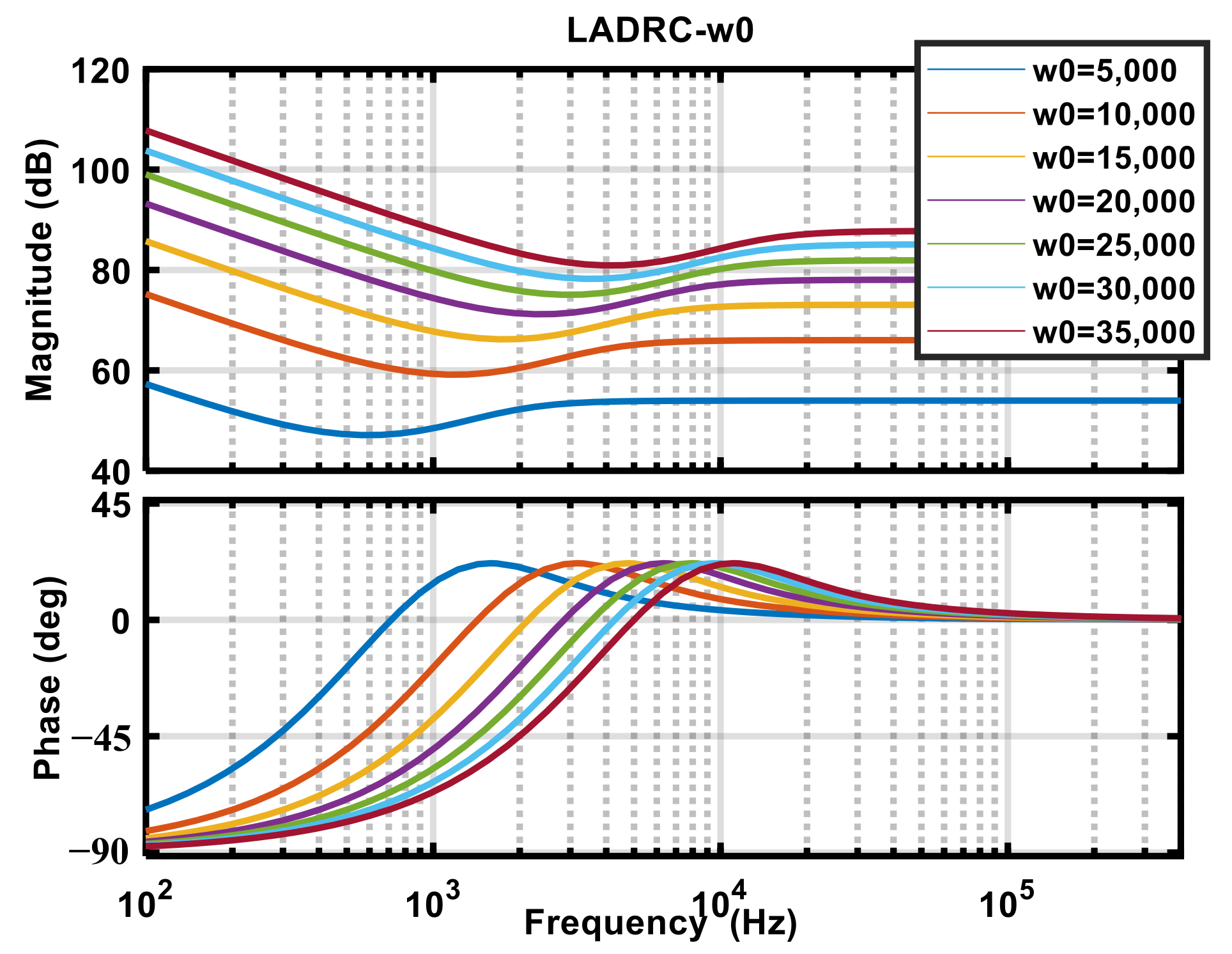
In engineering design,
ω0 = 2~10
ωc is usually selected to determine
ωc. With
b0 = 8000 unchanged and
ω0 gradually increased, the corresponding Bode diagram of the controller is drawn as shown in
Figure 6.
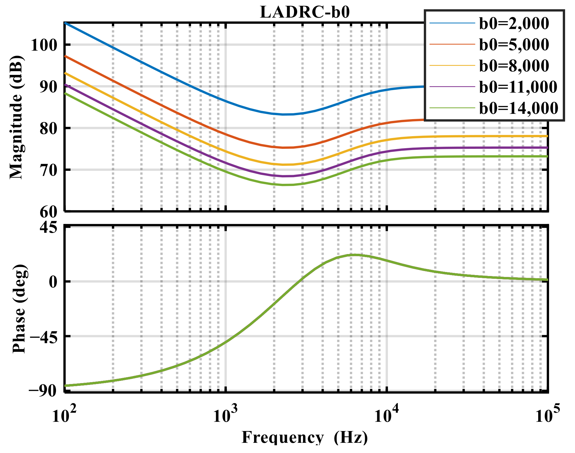
It can be seen that the controller gain increases gradually with the increase of ω0. Take ω0 = 20,000; gradually increasing b0, plot the Bode as follows:
As shown in
Figure 7, the overall gain of the controller gradually decreases with the increase in
b0. By changing the values of
b0 and
ω0 to observe the control effect, and combining the constraint relationship between
ω0 and
ωc, the relevant parameters of the controller are finally determined in
Table 2:
To realize the LADRC algorithm in DSP better, taking
d-axis as an example, the realization flow of controller is deduced. From the LESO output results, calculate the error between the given reference signal
Udref and the state estimate:
State feedback control law:
Disturbance compensation:
The formula for the target voltage vector
Ud can be converted into the following:
The DSP28034 used is a 32-bit fixed-point computing processor with a main frequency of 60 MHz. To ensure the real-time performance of the control algorithm, floating-point arithmetic is transformed into fixed-point arithmetic through IQ_Math library to improve the arithmetic speed. DMA is used to transmit data and reduce CPU load. Finally, the redundant data are cleared in real time.
4.2. Driver Circuit Design
The GaN switch tube used in the prototype is driven by a voltage range of −10~7 V. There is parasitic inductance in the gate drive loop of GaN devices. In addition to the parasitic capacitance of GaN devices,
UGS is prone to voltage spikes and oscillations in high frequency operating environments. This is not conducive to the normal operation of GaN devices, and in serious cases, it will lead to GaN devices exploding tubes [
14]. The main reasons for voltage spikes and oscillations in GaN device
UGS are as follows:
Lg and parasitic capacitors (
CGS,
CGD) constitute
LC resonant circuits. When the drive signal jumps, the step response of
UGS can be modeled as a second-order
RLC oscillator circuit, whose transfer function is as follows:
where
Udrv is the driving voltage. The damping ratio
ζ can be obtained by the transfer function, and the damping ratio determines whether
UGS oscillates:
If ζ < 1, the system is underdamped and UGS oscillates. If ζ ≥ 1, the system is critically damped or overdamped, and the oscillation is suppressed.
Based on the above analysis, the voltage spike of GaN device,
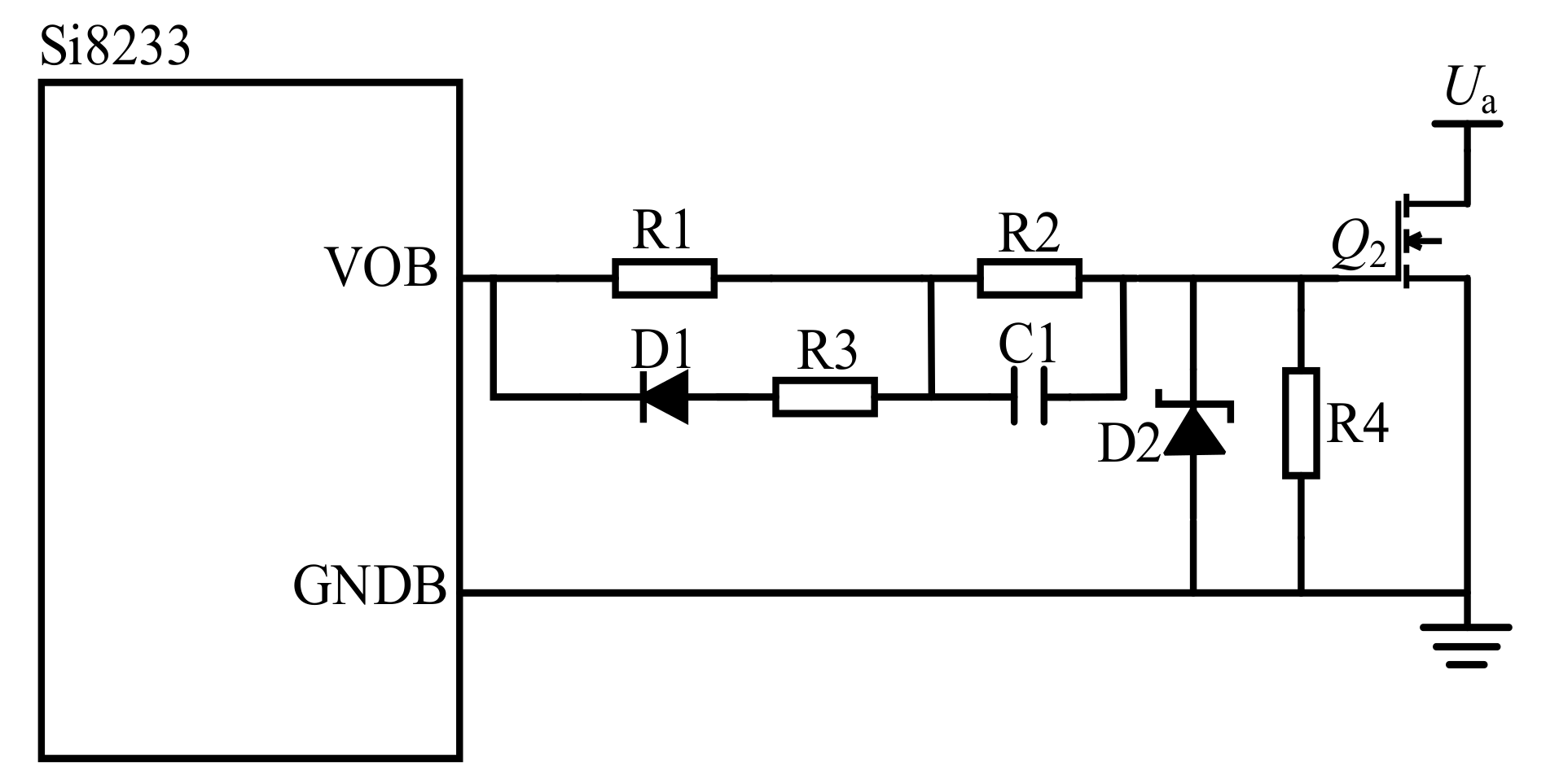
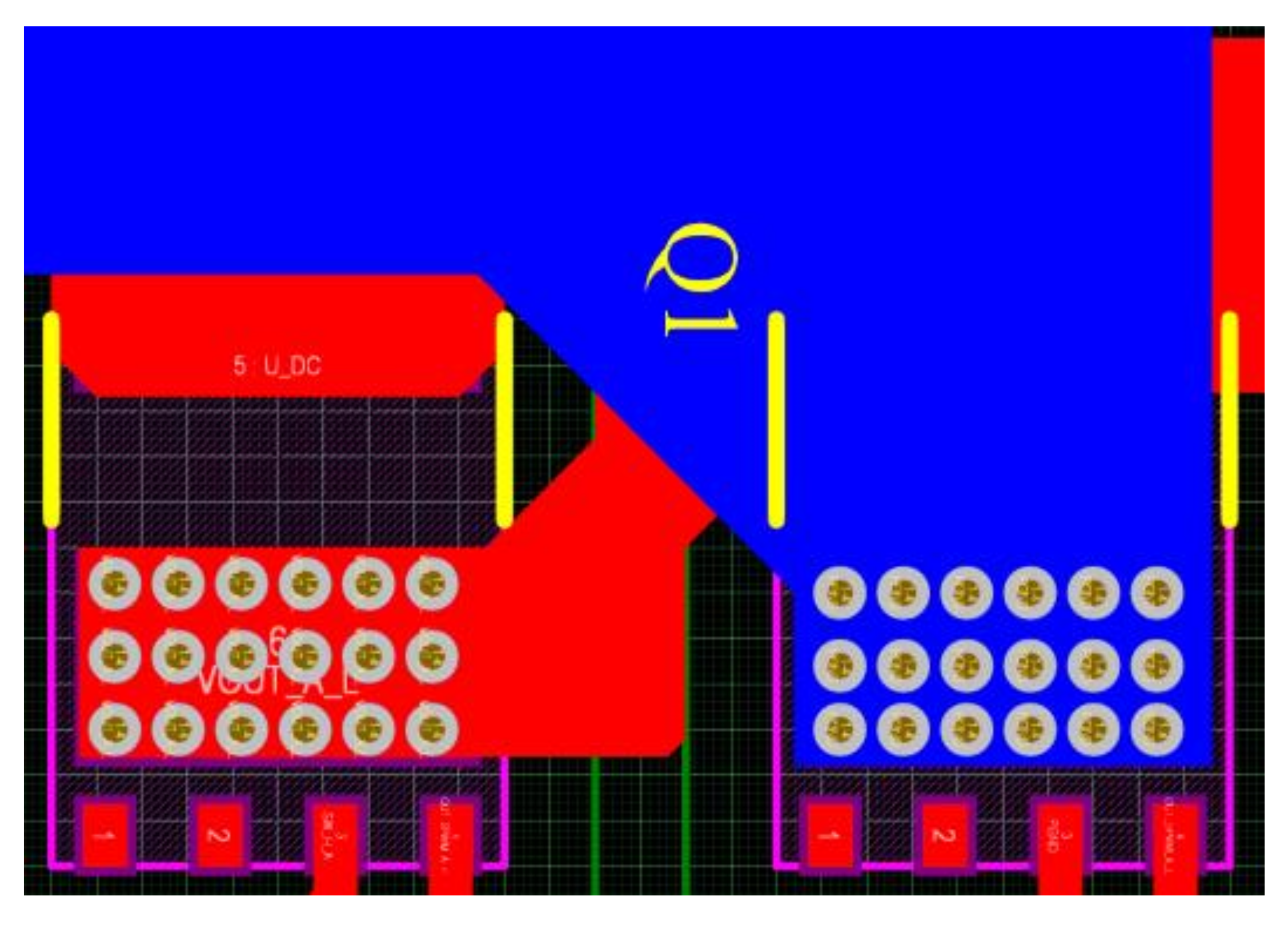
UGS, is absorbed by an external buffer circuit. In this paper, a simple and practical buffer circuit is designed. The buffer circuit and GaN device driver circuit constitute a new driver circuit. Taking the Q2 tube as an example, the driving circuit design is shown in
Figure 8 below.
R1 is the on resistor and R3 is the off resistor. At the same time, the S pole is led back to the GNDB pin of the chip as a reference voltage. When the upper tube is driven, the pin is connected to the input power supply of the driver chip through the bootstrap capacitor to raise the upper tube drive voltage and ensure that the UGS of the high side tube meets the requirements through the bootstrap mode.
Diode D1 is a single-channel device. In the circuit, when the drive signal is transmitted forward, diode D1 is switched on, allowing the current to pass through. When there is a reverse voltage (such as the reverse electromotive force that may be generated in the moment when the GAN device is turned off), diode D1 shuts off to prevent the reverse current from causing damage to the driver chip or other devices and plays a role in protecting the circuit.
C1 and resistor R2 constitute RC filter circuits, which are mainly used to absorb voltage spikes generated by parasitic capacitance when driving the waveform is on and off. It can filter out high-frequency noise and interference in the drive signal, make the drive signal smoother and more stable, and improve the reliability of gallium nitride devices. At the same time, the capacitor C1 can also play a certain role in charge storage and release during the switching moment of the gallium nitride device, helping to stabilize the gate voltage.
D2 is a voltage regulator used to rapidly drain the charge from the gate of gallium nitride devices. When the gallium nitride device needs to be turned off, D2 quickly switches on, quickly releases the charge on the gate, accelerates the turn-off speed of the gallium nitride device, improves the switching performance of the circuit, and prevents the gate from appearing overvoltage.
R4 is a shunt voltage regulator resistor connected between the G and S terminals. It ensures reliable operation of GaN devices during switching and enhances overall circuit performance and stability by limiting gate current, stabilizing gate voltage, suppressing spikes, and optimizing switching characteristics.
5. Simulation Analysis
On the basis of the above control strategy, a Simulink simulation model is built, and the active disturbance rejection controller is used to track the d- and q-axis voltages. The load and LCL filtering parameters are set in
Table 3.
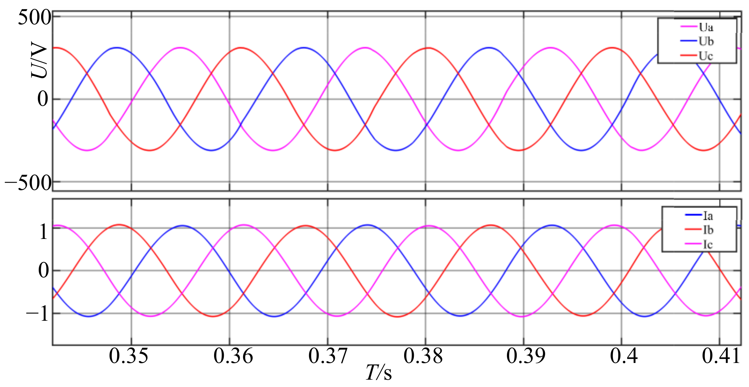
The system is connected to a 500 W three-phase load.
Figure 9 shows the simulation output voltage and current waveforms at the rated power.
As can be seen in the output waveform in
Figure 9, the linear active disturbance rejection control still has a good control effect at 200 kHz, thus meeting the use requirements at a high frequency.
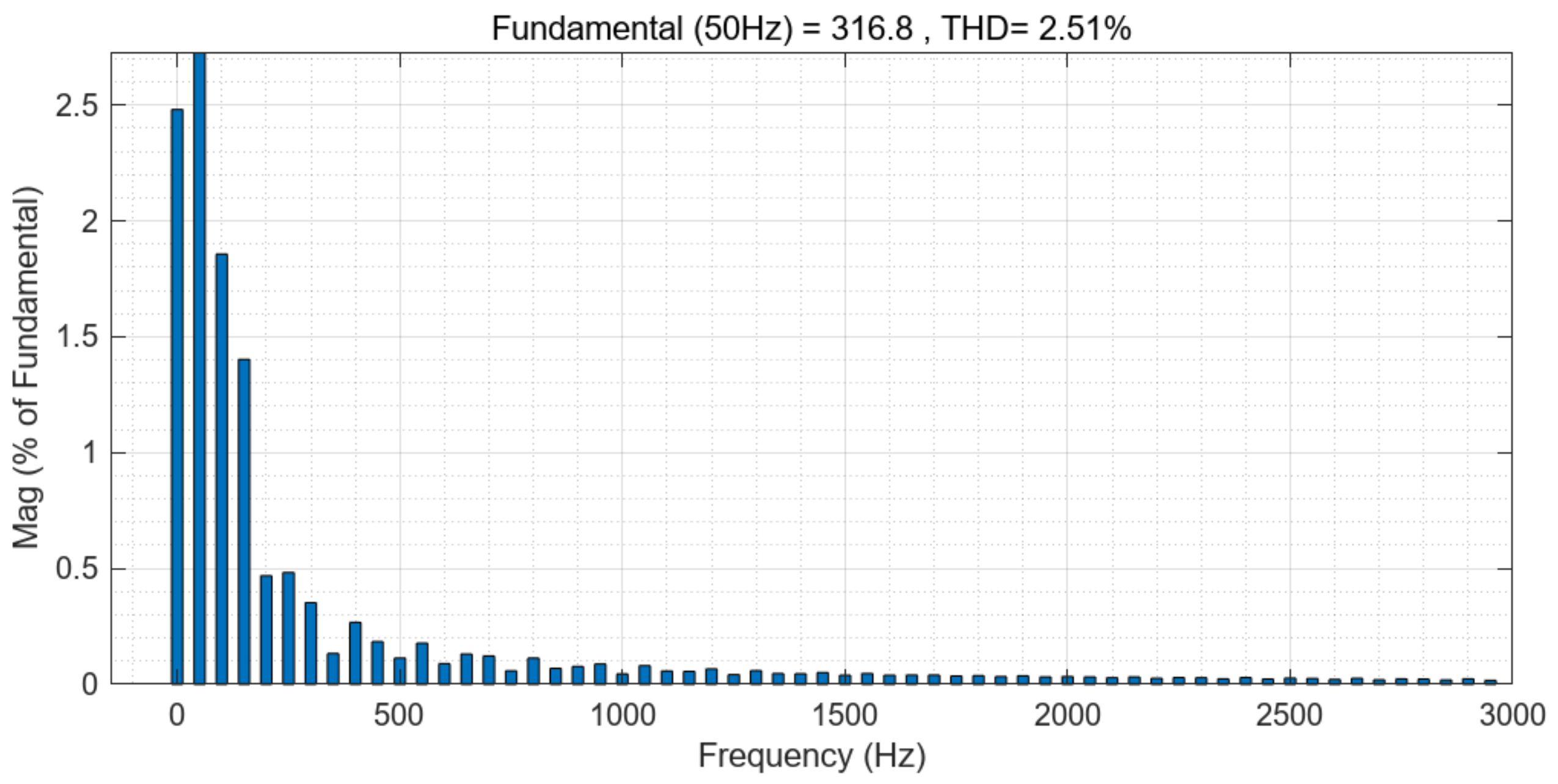
The harmonic analysis of output voltage is carried out by using FFT tool built in POWERGUI in Simulink platform. The corresponding voltage output harmonics THD are calculated as shown in
Figure 10:
As can be seen from
Figure 10, output harmonics THD = 2.51% < 5%, indicating that LADRC has a good suppression effect on harmonics in high-frequency inverter.
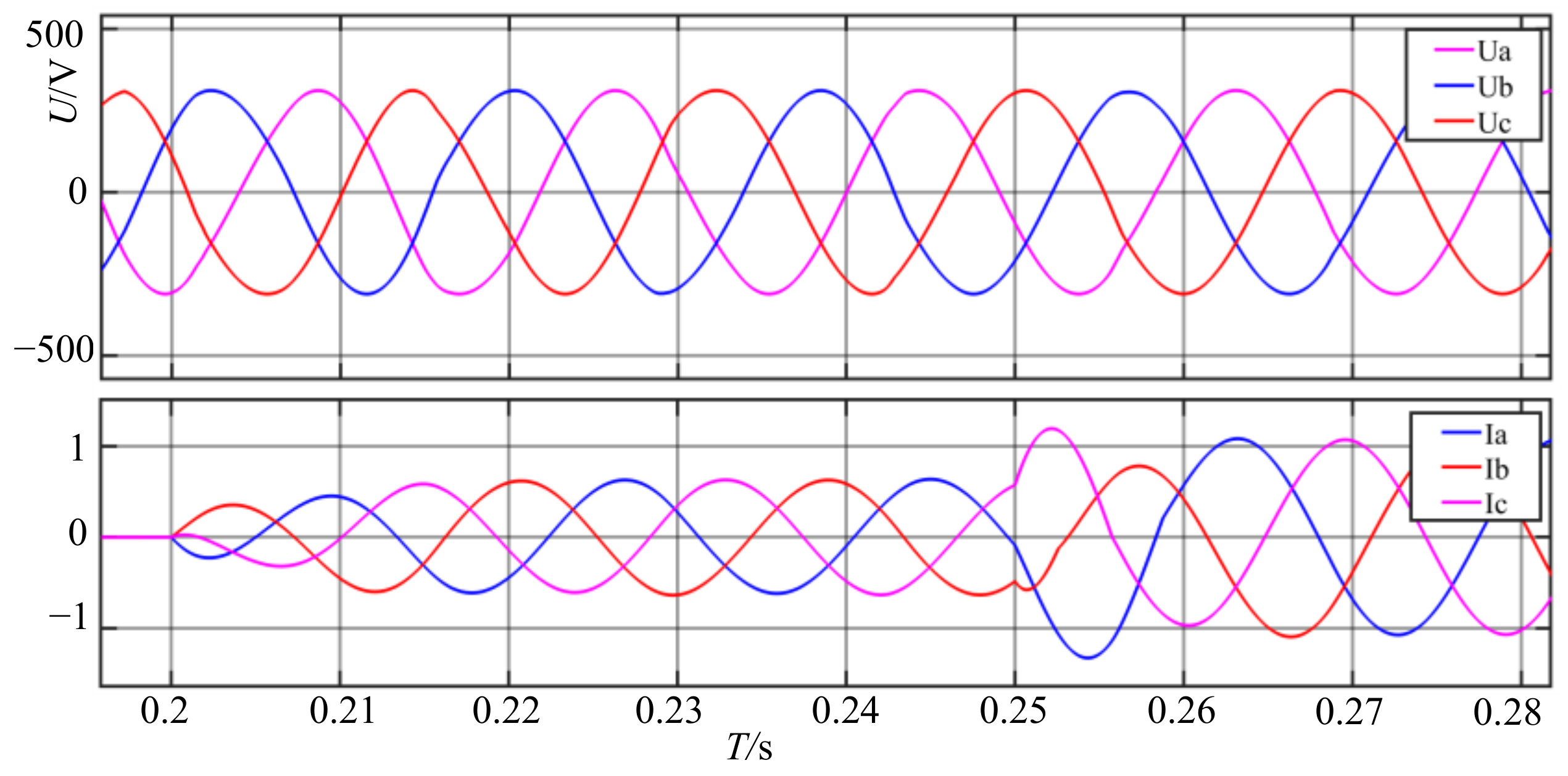
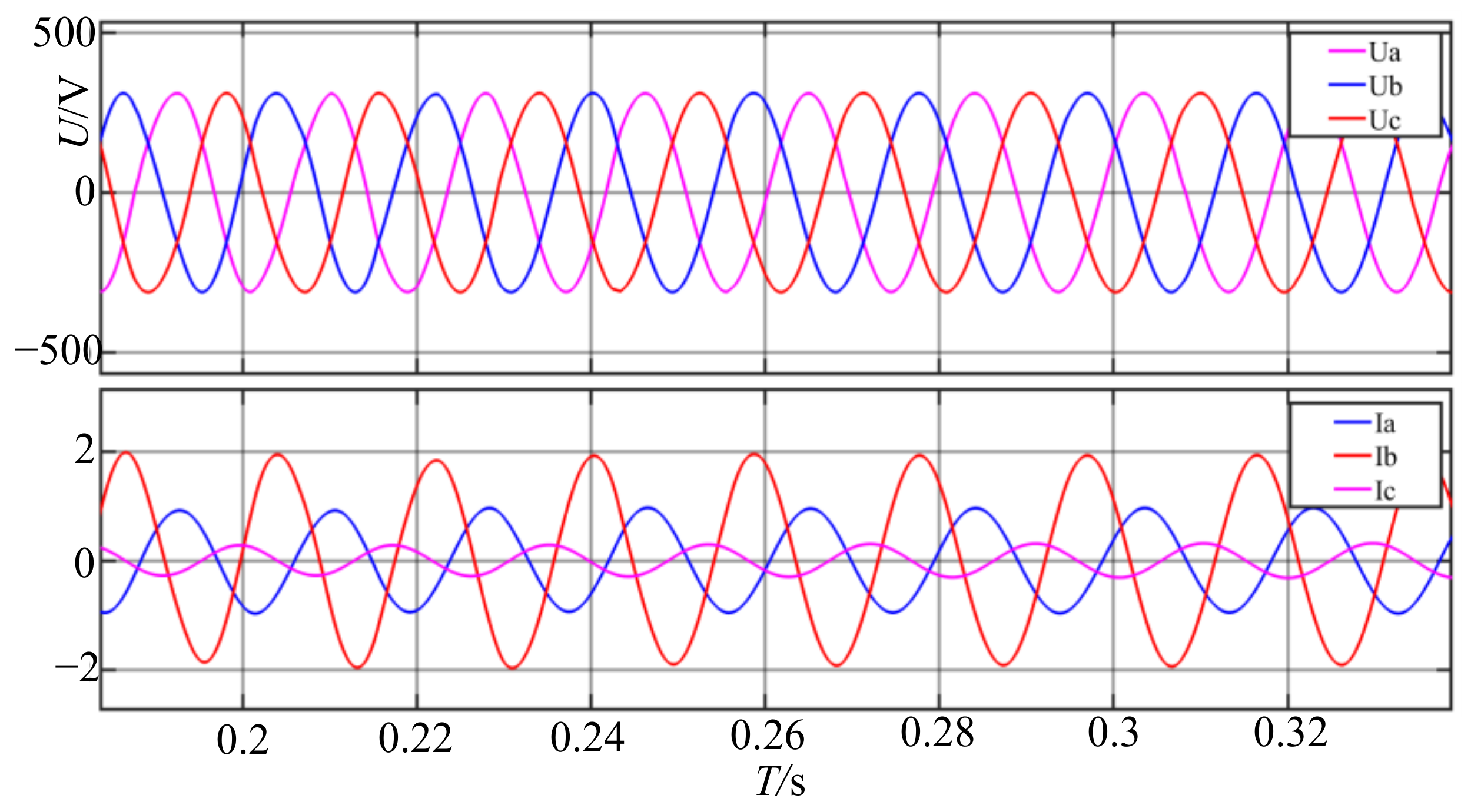
The load is switched from no load to a light load when T = 0.2 s and from a light load to a full load when T = 0.25 s; the system simulation output voltage and current waveforms are shown below.
As can be seen in
Figure 11, when the different loads are switched between
T = 0.2 s and
T = 0.25 s, the output voltage does not fluctuate significantly, the output current can respond quickly, and the subsequent output is stable, thus proving the effectiveness of the control strategy.
The three-phase unbalanced load access system is used for testing, and the output voltage and current waveforms are shown in
Figure 12 below.
As can be seen in
Figure 12, under the three-phase unbalanced load, the system can still work normally, and the output voltage and current waveforms are stable. This shows that the system has strong adaptability and robustness under linear active disturbance rejection control.
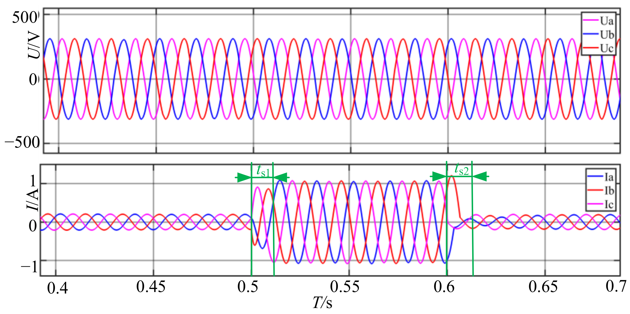
Then, the transient highly inductive load response is tested. Set at 0.5 s when the load is switched back to 20% from 20% to 100% (500 W) for 0.1 s. The reactive power of inductive load is set
QLA =
QLB =
QLC = 100 var. Record the output voltage and current waveform as shown in
Figure 13:
It can be seen from
Figure 13 that the adjustment time
ts1 ≈ 0.013 s and
ts2 ≈ 0.017 s when the highly inductive load changes abruptly. It shows that LADRC has good anti-disturbance ability in high frequency control.
Next, a three-phase, three-wire inverter simulation model and a controller simulation model are built. The effect of the control strategy is tested at 200 kHz in various experiments, such as load hopping experiments, and the feasibility and effectiveness of the control strategy are verified.
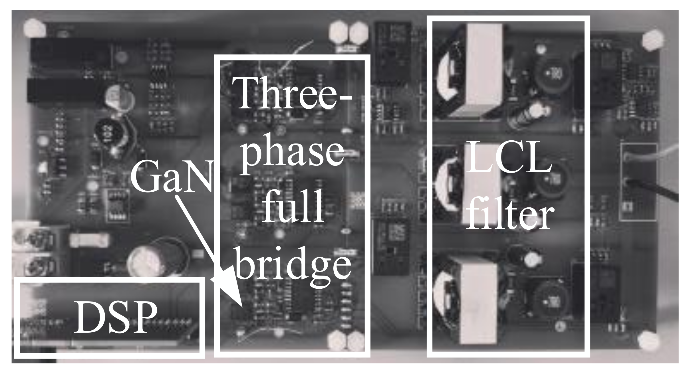
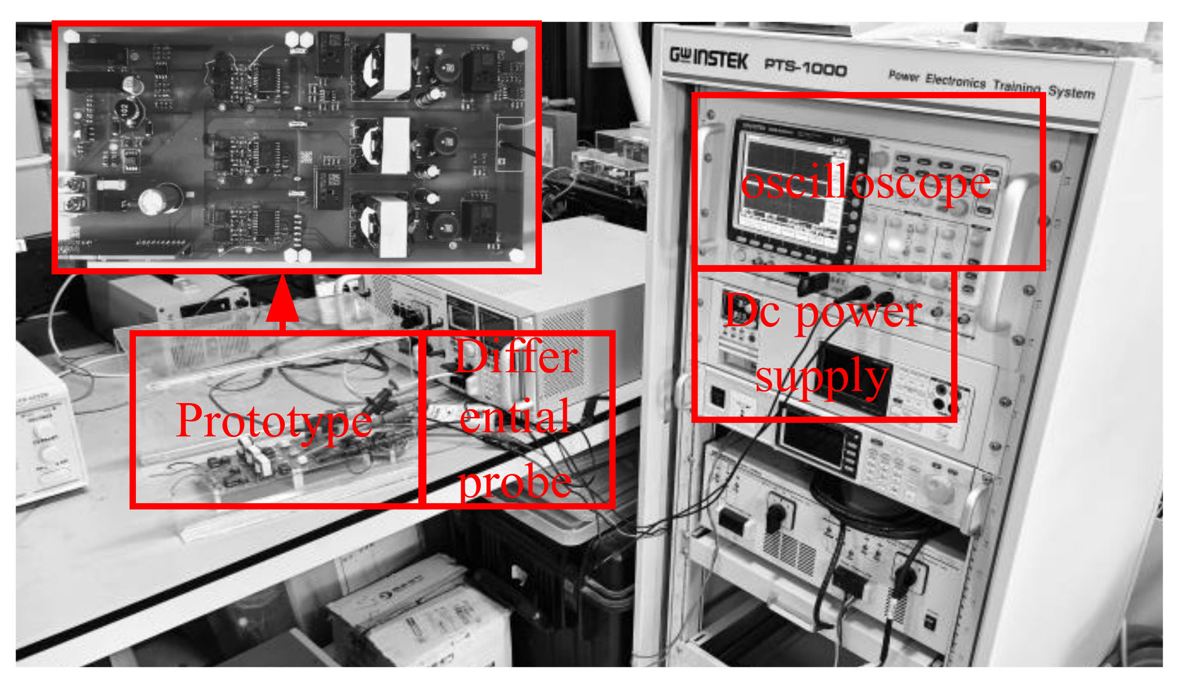
6. Experimental Verification
A 500 W gallium nitride three-phase digital inverter is built based on GaN power devices. The specifications of the selected GaN power devices are shown in
Table 1. The main control is DSP28034, which adopts space vector modulation technology (SVPWM). The main equipment used in the experiment are a DC power supply, oscilloscope, high-voltage differential probe, and gallium nitride three-phase inverter prototype. The built prototype and experimental test environment are shown in
Figure 14 and
Figure 15.
Considering the heat dissipation problem, when designing the PCB, copper is laid on the bottom of the GaN power device to facilitate heat dissipation. Thermal grease and heat sink are added on GaN power device during experimental tests as shown in
Figure 16 below:
First, the drive circuit is tested, with a switching frequency of
fsw = 200 kHz and phase A taken as an example. The upper and lower gate source voltage
UGS is measured by the oscilloscope probe. The source voltage UGS waveforms of the upper tube and lower tube gate in phase A are shown in
Figure 17.
It can be seen from
Figure 17 that the gate-source voltage is
UGS = 6.6 V, thus meeting the driving requirements of the GaN power devices used. The upper and lower tube drive dead zone time is set as shown in
Figure 18.
fsw = 200 kHz, period
T = 5 us, the dead zone is 1.66%, and the dead zone time is about 83.3 ns. According to the GaN power device parameters given in
Table 1, turn-on delay
td_on = 5 ns, turn-off delay
td_off = 8 ns. Query the data manual of the driver chip. Propagation delay
tprop = 5 ns. Keep the margin of
tmargin = 10 ns and calculate the minimum dead zone time.
The minimum dead zone time DTmin = 18 ns < 83.3 ns can be calculated by substituting the data.
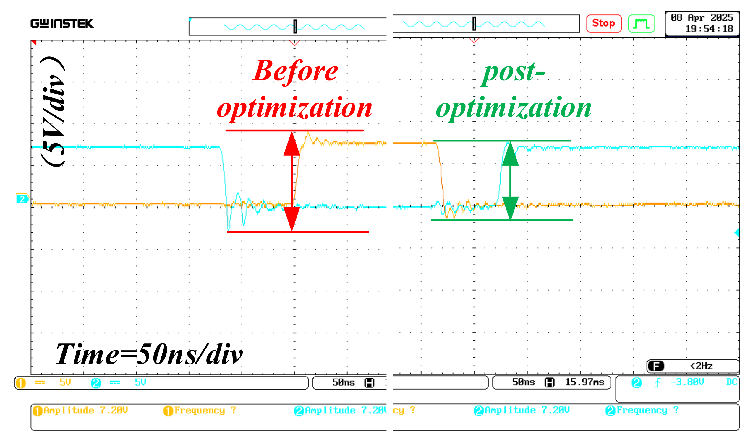
Compared with the drive circuit waveform before optimization, it can be seen from
Figure 19 that the voltage peak of the designed drive circuit is significantly improved. The on and off is smoother, and voltage overshoot and oscillation are significantly weakened, conducive to a high-frequency switching tube drive.
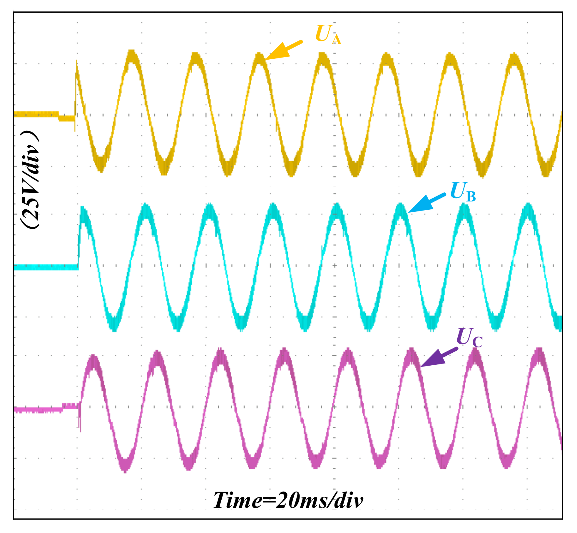
In the no-load state, the output voltage waveforms of
UA,
UB, and
UC are tested, as shown in
Figure 20.
As can be seen from
Figure 20, the three-phase waveform output of the GaN three-phase inverter prototype is relatively ideal, and the output amplitude does not fluctuate and distort significantly. The output frequency is stable at 50 Hz, and the three-phase phase is normal. The correctness of the prototype design is proved.


