1. Introduction
The IPT system enables contactless power transmission, offering distinct advantages in safety, reliability, and maintenance convenience compared to plug-in power supply methods [
1,
2,
3]. In recent years, IPT technology has gained widespread adoption across multiple domains, including electric vehicles, automated guided vehicles, and smartphones [
4].
Load variations adversely affect transmission efficiency and output voltage stability during the practical operation of the IPT system. To address this challenge, researchers globally have conducted focused investigations across three primary domains: impedance matching optimization, constant voltage control implementation, and enhancement of composite control strategies [
5,
6,
7,
8].
In the field of impedance matching research, ref. [
9] proposed an efficiency optimization method based on full-current-mode impedance matching, which utilizes a Buck converter for impedance matching on the secondary side of the IPT system. However, this control method has a limited impedance matching range. In the work of [
10], a four-switch Buck–Boost circuit for impedance matching was employed on the secondary side of the IPT system. Still, this impedance matching circuit exhibits a complex structure and higher costs.
In the field of constant voltage control research, Ref. [
11] analyzed different topologies to derive the impact of parasitic parameters on output characteristics, achieving stable output voltage regulation through primary-side control. However, this control method exhibits a relatively large load regulation rate. Ref. [
12] implemented a three-level buck circuit on the secondary side of the IPT system, proposing a composite control strategy that integrates active disturbance rejection control with a disturbance observer. In Ref. [
13], a composite observer design is proposed considering the impact of high-frequency noise on ADRC. This design predicts the output voltage and current of the secondary-side Buck circuit through state prediction to suppress high-frequency noise interference. Ref. [
14] proposes a composite anti-disturbance control strategy that achieves constant voltage control in an IPT system by introducing sliding mode control and integrating it with an extended state observer.
In the research on composite control strategies, Ref. [
15] achieves maximum efficiency tracking by controlling the phase-shift angle of the inverter on the primary side of the IPT system while implementing constant voltage control on the secondary side via a Buck–Boost circuit. However, the secondary-side controller employs a PID controller, which exhibits limited disturbance rejection capabilities. Ref. [
16] similarly utilizes phase-shift control for maximum efficiency tracking on the primary side. A T-S fuzzy event-triggered H
∞ control framework is proposed for secondary-side constant voltage control, significantly enhancing disturbance rejection performance. Ref. [
17] addresses the low efficiency of IPT systems under light-load conditions by designing a sensorless observer. This observer estimates the AC equivalent load, which is then integrated with a maximum efficiency tracking control algorithm to achieve optimal efficiency. Ref. [
18] analyzes the efficiency degradation of LCC-S topology-based IPT systems under load fluctuations and proposes a primary-side variable inductance-based constant-current output control. Additionally, maximum efficiency tracking is realized by adjusting the conduction angle of the secondary-side rectifier circuit. Ref. [
19] improves system efficiency by regulating the secondary-side variable inductance while enabling seamless switching between constant voltage and constant current modes through a secondary-side Boost circuit.
Based on the above analysis, to rapidly suppress output voltage fluctuations under load transients and realize maximum efficiency tracking in IPT systems, this paper proposes a composite control strategy integrating maximum efficiency tracking with an improved ADRC for IPT systems. By analyzing the relationship between the maximum efficiency operating point of the LCC-S-compensated IPT system and the duty cycle of the secondary-side DC-DC converter, the primary-side Buck converter is utilized to regulate the duty cycle of the secondary-side DC-DC converter, thereby achieving maximum efficiency tracking.
An improved active disturbance rejection controller is proposed for constant voltage control to enhance the IPT system’s dynamic voltage regulation capability. The composite control strategy, combining these two methods, ensures that the IPT system operates at the maximum efficiency point while rapidly suppressing output voltage fluctuations under large load variation scenarios.
2. System Analysis and Maximum Efficiency Tracking Control
The circuit diagram of the LCC-S IPT system is shown in
Figure 1. The Buck circuit consists of a capacitor
Ca, power semiconductor switch
Sa, diode
Da, inductor
La, and capacitor
Cb. The inverter converts DC power into high-frequency AC power, with the LCC-S compensation network formed by
LR,
CP,
CR, and
CS.
LP,
LS,
M,
RP, and
RS represent the self-inductance of the transmitting coil, self-inductance of the receiving coil, mutual inductance between coils, internal resistance of the transmitting coil, and internal resistance of the receiving coil, respectively. The rectifier converts high-frequency AC power back to DC power. Components
Cc,
Sb,
Ct,
Lb,
Lc, and
Cd constitute the Zeta circuit. The load resistance is denoted as
RL.
The primary-side Buck circuit indirectly adjusts the duty cycle of the secondary-side DC-DC circuit to achieve maximum efficiency tracking. The gain range of the secondary-side DC-DC circuit should be maximized to accommodate efficiency optimization across wide load ranges. Among non-isolated DC-DC topologies, both Buck–Boost and Zeta circuits can achieve bidirectional voltage conversion. In most power conversion applications, consistent input–output voltage polarity is required. Compared with the Buck–Boost configuration, the Zeta circuit maintains identical input–output voltage polarities while exhibiting reduced current stress and enhanced conversion efficiency. Therefore, this paper adopts the Zeta circuit for the implementation of secondary-side constant voltage control.
2.1. Efficiency Analysis of LCC-S Inductive Power Transfer System
Based on the fundamental harmonic analysis method, the mutual inductance model of the LCC-S IPT system is illustrated in
Figure 2, where
denotes the inverter output voltage;
,
, and
represent the currents of the resonant inductor, transmitting coil, and receiving coil, respectively; and
Req corresponds to the AC equivalent load.
Based on Kirchhoff’s Voltage Law, the circuit equations of the mutual inductance model are derived as follows:
In the Equations,
denotes the resonant angular frequency of the system. When the circuit operates under resonant conditions, the following relationship is satisfied:
Therefore, the voltage gain
and transmission efficiency
of the LCC-S IPT system can be derived as
By setting
, the AC equivalent load
corresponding to the maximum efficiency operating point
of the IPT system is derived as
2.2. Control Strategy for Maximum Efficiency Tracking
Based on the analysis above, the IPT system operates at the maximum efficiency point when its AC equivalent load equals . To ensure both maximum efficiency tracking and constant output voltage under varying load conditions, the primary-side Buck circuit adjusts the input voltage of the inverter, thereby modifying the rectifier output voltage. Since the Zeta circuit inherently maintains a constant output voltage under steady-state conditions, its duty cycle dynamically adapts to the rectifier output voltage variation. This adaptation mechanism effectively regulates the AC equivalent load , enabling real-time maximum efficiency tracking.
Assuming the Zeta circuit operates in continuous conduction mode and neglecting its power losses, the output impedance
of the rectifier is expressed as
In the equations,
D represents the duty cycle of the Zeta circuit. Since the secondary-side rectifier is a full-bridge configuration, the relationship between the AC equivalent load
and the rectifier output impedance
is expressed as
When the AC equivalent load
satisfies the following condition:
When the system operates at the maximum efficiency point, by simultaneously solving Equations (5)–(7), the duty cycle
of the Zeta circuit required to achieve maximum efficiency tracking in the IPT system is derived as
Let
and
denote the output voltages of the Zeta circuit and the rectifier, respectively. Thus, the following relationship holds:
By adjusting the output voltage
of the Buck circuit, the output voltage
of the rectifier is regulated, thereby controlling the duty cycle
equals
of the Zeta circuit. Combining Equations (3), (8) and (9), the inverter output voltage
must satisfy the following condition:
The primary-side inverter adopts a full-bridge configuration. Therefore, the reference voltage of the Buck circuit is determined as follows:
By regulating the output voltage
of the Buck circuit to match the reference voltage
, maximum efficiency tracking is achieved on the primary side. The designed control block diagram for maximum efficiency tracking is shown in
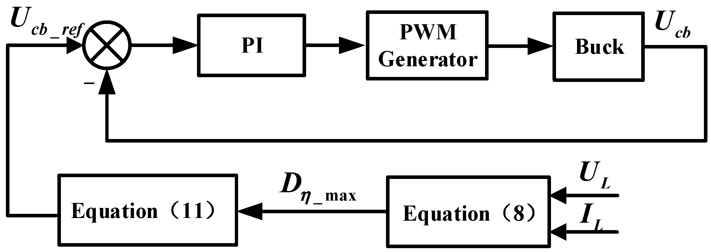
Figure 3.
In
Figure 3, as load
and
vary, the Bluetooth communication module transmits the real-time output voltage
and current
of the Zeta converter to the Buck circuit controller. The equivalent load resistance
equals
. The target duty cycle
is subsequently computed using Equation (8), followed by the derivation of the Buck converter’s reference voltage
based on Equation (11). Considering that maximum efficiency tracking requires no fast dynamic response, a proportional-integral controller provides adequate performance for achieving maximum efficiency tracking in the IPT system through Buck converter regulation.
3. Controller Design and Stability Analysis
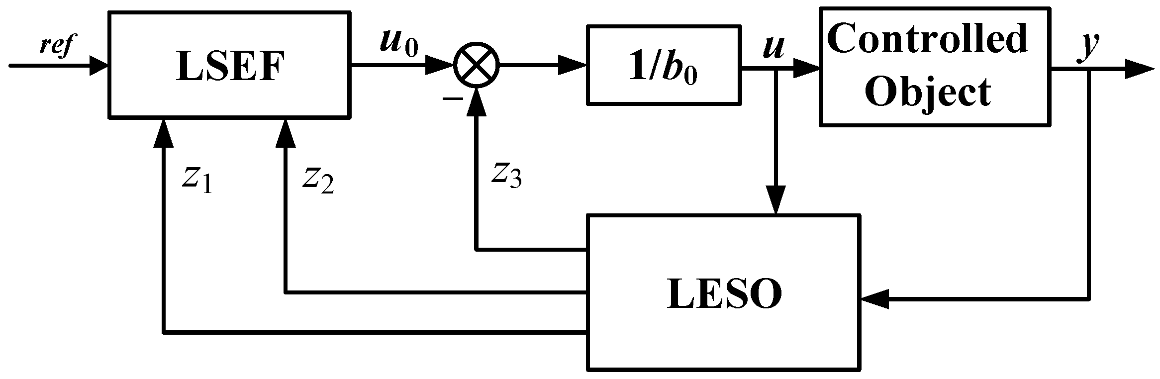
The core concept of ADRC lies in real-time estimation and compensation of system disturbances through dedicated observers, thereby effectively attenuating their operational impacts [
20]. As illustrated in
Figure 4, LADRC architecture is implemented for secondary-side constant voltage regulation of the Zeta converter in the IPT system. This advanced controller comprises three essential components:
A linear extended state observer (LESO) for simultaneous tracking of system states and disturbance estimation;
Disturbance compensation module with feedforward cancelation;
Linear state error feedback (LSEF) control law generating the final actuation signal.
In
Figure 4,
,
, and
are observed variables,
is the reference quantity,
y is the controlled object output,
b0 is the controller gain, and
u is the controller output.
3.1. Linear Extended State Observer Design
To ensure output voltage stabilization of the IPT system across broad load fluctuation ranges, a Zeta converter is employed on the secondary side for voltage regulation. The state-space averaged model of the Zeta converter is formulated as follows [
21]:
In the equation,
represents the current flowing through inductor
,
denotes the current flowing through inductor
, and
is the voltage across capacitor
. The Zeta circuit is a fourth-order system, which increases the complexity of controller design. To simplify the design, it is necessary to reduce the order of the Zeta circuit [
22]. By setting
equals
, a second-order model of the Zeta circuit is obtained:
For ease of analysis, Equation (13) is reformulated into the following form:
In the Equation,
,
, and
are the corresponding system parameters,
represents the external disturbance,
is the duty cycle
D of
, and
y denotes the output voltage of the Zeta circuit. Based on the above formulation, the corresponding LESO is designed as follows:
In the Equation,
,
f represents the total disturbance that combines both external and internal disturbances. Following the method in [
23], the LESO characteristic equation is configured at
using the pole placement method, where
denotes the observer bandwidth. The observer matrix corresponding to Equation (15) is given by
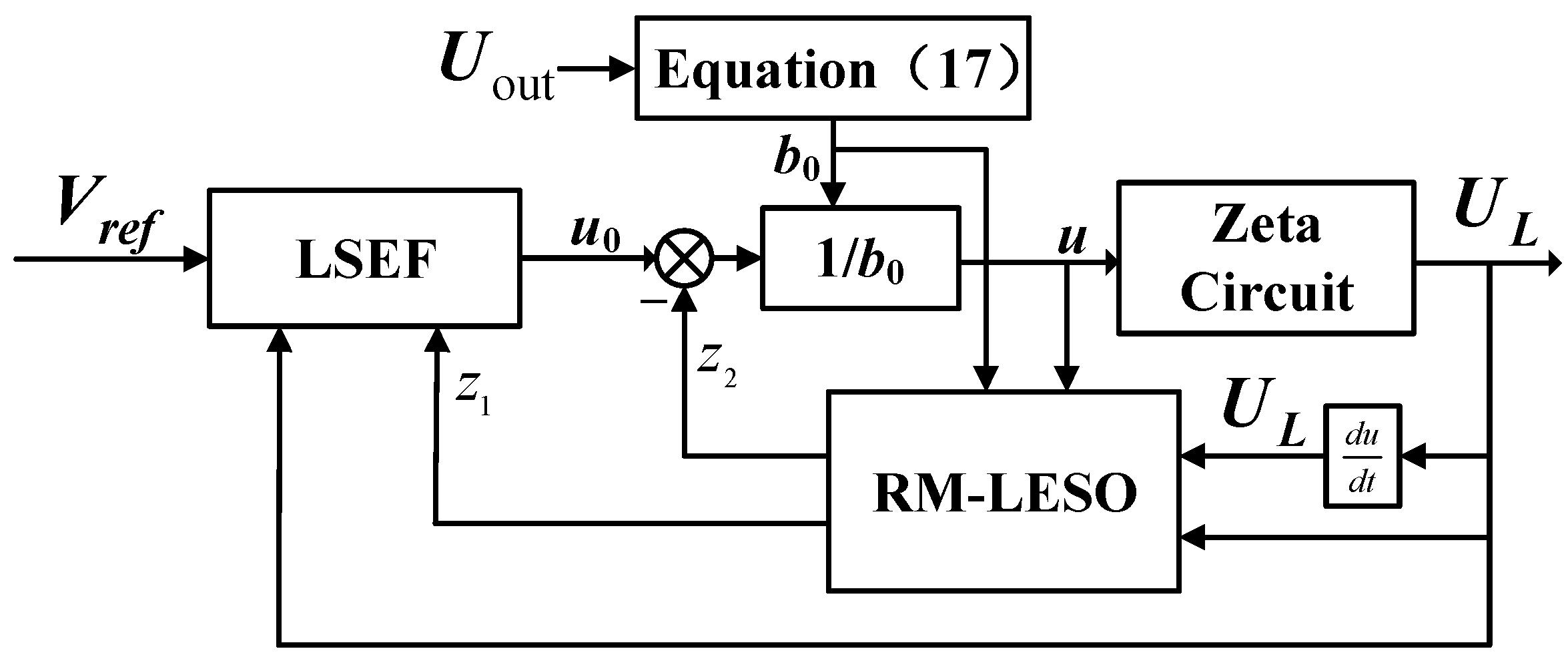
3.2. Model-Assisted Reduced-Order LESO Design
A reduced-order design is implemented to enhance the LESO’s convergence rate and reduce its computational complexity. Since the Zeta circuit’s output voltage
can be measured accurately, it is unnecessary to estimate
. Instead, the derivative of the output voltage
is utilized as feedback, resulting in a reduced-order linear extended state observer (R-LESO).
For system with partial prior knowledge of the model, integrating these known dynamics into the LESO can either reduce the required observer bandwidth or enhance disturbance estimation accuracy without sacrificing bandwidth, thereby improving overall control performance [
24]. Based on the preceding analysis of the Zeta circuit, the known terms are
The parameter
b0 denotes the controller gain. Since the rectifier’s output voltage
Uout can be directly measured, tuning is not required. Leveraging model-assisted knowledge, the observer matrix for the LESO is designed as follows:
Since
can be directly measured, a reduced-order reformulation of Equation (19) is implemented, resulting in the reduced-order model-assisted linear extended state observer (RM-LESO).
To simplify the controller design, the poles of the RM-LESO characteristic equation are placed at
via pole placement, and the observer gain matrix is given by
Since the system disturbances can be estimated and compensated, the error integral term is no longer required. The LSEF is designed as
In the equation,
denotes the reference voltage, while
and
represent the proportional gain and derivative gain, respectively. According to the parameterization configuration method,
is the square of
and
is set as
, where
is the controller bandwidth. The block diagram of the proposed reduced-order model-assisted linear active disturbance rejection control (RM-LADRC) is illustrated in
Figure 5:
3.3. Controller Parameter Analysis
Taking the Laplace transform of Equation (20) yields the Laplace-domain expression of the observed variables:
Taking the Laplace transform of Equation (14), the relationship between the system output
y and the total disturbance
f is derived as follows:
By combining Equations (23)–(25), the transfer function of the RM-LADRC is derived as follows:
In the equation, the parameters
and
are introduced to simplify the transfer function expression. From Equation (26), it can be observed that the system output comprises both the reference term
and the disturbance term
f. When the reference term is neglected, the system output solely reflects the disturbance term, yielding the disturbance-to-output transfer function of the RM-LADRC as follows:
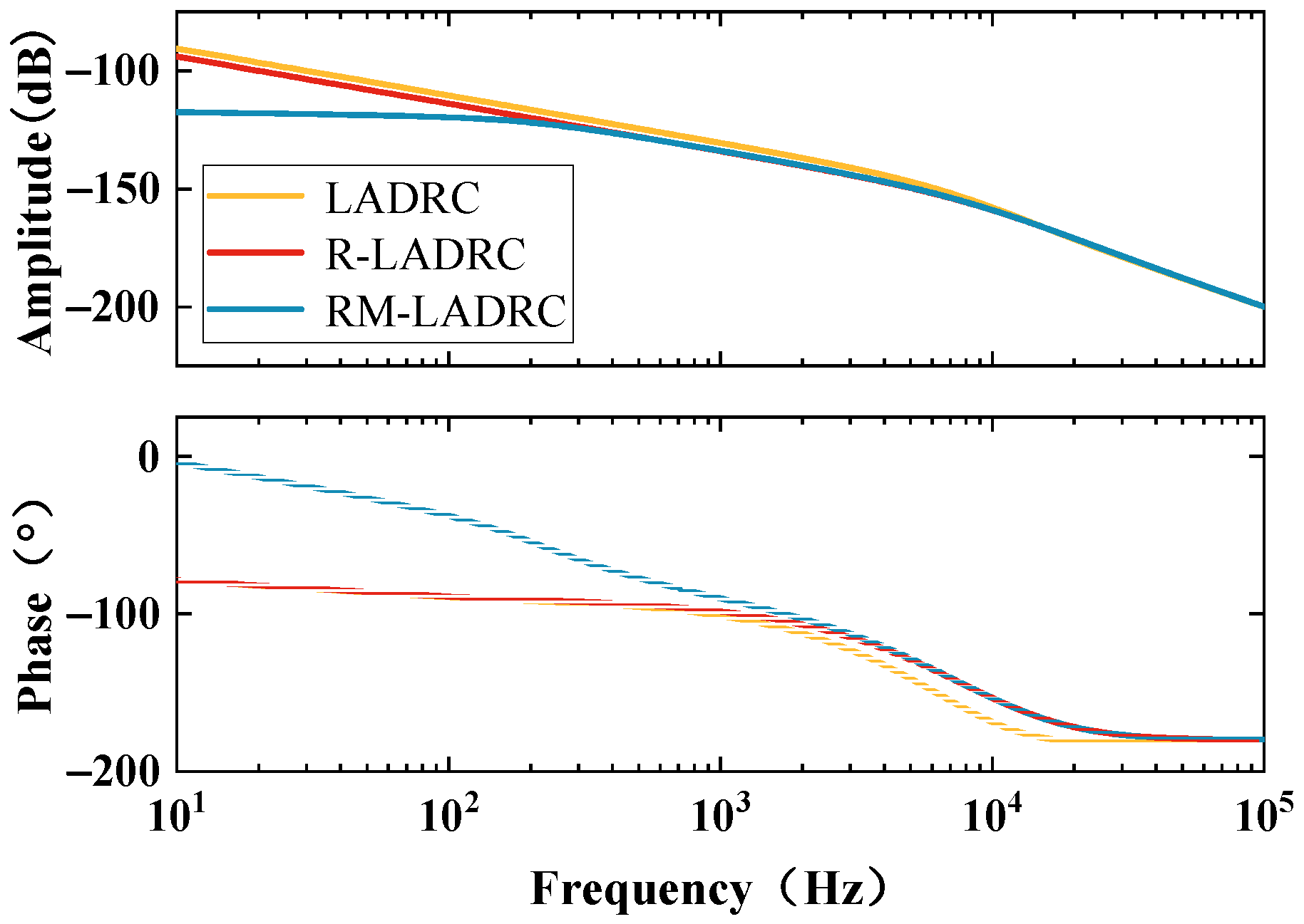
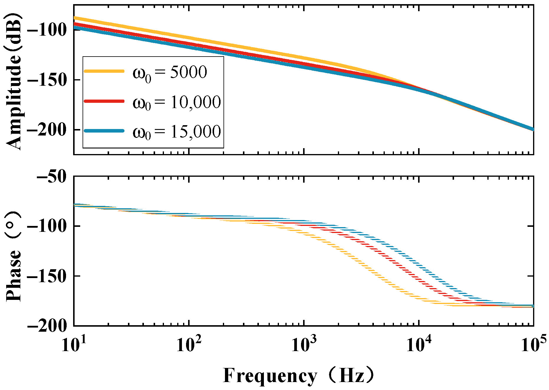
Figure 6 shows the comparison of frequency domain characteristics of different LADRC disturbances.
Figure 6 reveals that compared to conventional LADRC, the R-LADRC demonstrates a slight reduction in mid-to-low frequency gain while exhibiting less phase lag in the mid-frequency range. Notably, the RM-LADRC shows significantly lower gain than both LADRC and R-LADRC in the mid-low frequency band, endowing it with superior disturbance rejection capability at lower frequencies. The phase lag characteristics of RM-LADRC substantially outperform those of LADRC and R-LADRC in the mid-low frequency range, with all three controllers exhibiting overlapping curves in the high-frequency domain. These findings demonstrate that observer order reduction and model information incorporation can effectively improve disturbance rejection characteristics in low-frequency regimes, enhance dynamic performance in mid-frequency ranges, and avoid high-frequency gain amplification.
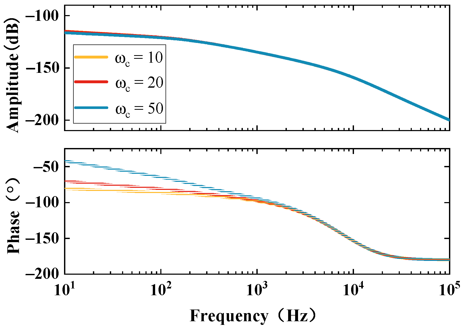
The frequency domain characteristics of RM-LADRC disturbances under different
values are comparatively presented in
Figure 7.
The observer bandwidth
primarily governs the gain characteristics of the LESO. An increased
leads to enhanced disturbance suppression efficacy, thereby strengthening the system’s rejection capability. Furthermore, in the mid-frequency range, the phase lag magnitude is progressively attenuated with higher
values, resulting in further refined dynamic response characteristics.A comparative analysis of RM-LADRC disturbance frequency-domain characteristics under different
values is systematically illustrated in
Figure 8.
Figure 8 demonstrates that increasing the controller bandwidth
reduces low-frequency gain magnitude, which enhances disturbance rejection capability. However, excessive bandwidth enlargement may compromise the phase margin and induce high-frequency instability. This requires adopting a progressive tuning strategy: initializing
at a low value, then gradually increasing it until attaining the desired dynamic response speed while ensuring adequate stability margins.
3.4. Controller Stability Analysis
The closed-loop transfer function from reference voltage
to output voltage
in the Zeta converter, as described in Equation (26), can be simplified to
The stability of the system can be determined via the Routh–Hurwitz stability criterion [
25]. The necessary conditions for system stability are expressed as follows:
By synthesizing Equation (29), the necessary and sufficient conditions for closed-loop system stability can be derived as follows:
As demonstrated by Equation (31), controller parameters and model fidelity may critically influence system stability. The design methodology necessitates a two-stage procedure: initial parameter tuning followed by stability validation via Equation (31) to ensure compliance with operational constraints. For instance, in the Zeta converter prototype studied herein, system instability manifests when load resistance falls below a critical threshold. Consequently, post-tuning verification must explicitly establish the allowable range of compatible with the designed parameters, thereby precluding instability induced by modeling inaccuracies or load excursions.
As comprehensively analyzed, the RM-LADRC design encompasses three critical parameters: , , and . Notably, is uniquely determined by Equation (18) through rigorous model derivation, thereby reducing the tuning effort to only two degrees of freedom: observer bandwidth and controller bandwidth .
To achieve the dual objectives of maximum efficiency tracking and constant voltage output in the IPT system,
Figure 9 delineates the architecture of the proposed hybrid control strategy, which synergistically integrates adaptive frequency tuning and phase-shift regulation.
In
Figure 9, the load resistance
can be calculated by measuring the output voltage
and output current
of the Zeta converter. These parameters (
and
) are transmitted to the primary-side Buck converter controller via Bluetooth communication. The maximum duty cycle
is calculated based on Equation (8), and the reference voltage
for the Buck converter is derived from Equation (11). By regulating the duty cycle of the Zeta converter through Buck circuit control, maximum efficiency tracking is achieved. The rectifier circuit output voltage
is sampled to determine the controller gain
, while parameter
defines coefficient
and duty cycle
D determines coefficient
. The constant voltage output of the IPT system is realized through the RM-LADRC controller. The combined control strategy integrating these two approaches enables the simultaneous implementation of maximum efficiency tracking and constant voltage output in the system.
4. Experimental Verification
To verify the effectiveness of the proposed control strategy, an IPT system experimental platform was constructed, as shown in
Figure 10. The platform consists of a DC power supply, electronic load (Chroma 63804, Chroma Systems Solutions, Taoyuan City, Taiwan, China), Buck converter, full-bridge inverter, LCC-S compensation network, magnetic coupling mechanism, rectifier, Zeta converter, and Bluetooth communication module (HC-06, Guangzhou HC information Technology Co., Ltd., Guangzhou, China). Experimental waveforms were recorded using an oscilloscope (DSO-X 2024A, Keysight Technologies, Santa Rosa, CA, USA) with a current probe (RP1001C, RIGOL Technologies, Beijing China) and a differential probe (RP1025D, RIGOL Technologies, Beijing China). The magnetic coupling mechanism employs circular coils wound with 16-turn (primary) and 18-turn (secondary) Litz wire, operating at an air gap distance of 50 mm.
4.1. Experimental Parameters
Table 1 summarizes the controller parameters employed in the experiments. The PI controller parameters were tuned using the PID Tuner toolbox in MATLAB/Simulink R2024b. In contrast, the parameters for the LADRC, R-LADRC, and RM-LADRC controllers were designed following the methodology outlined in [
18]. The design objective prioritized zero overshoot and minimized settling time during the step reference voltage transition from 0 to 24 V for the Zeta converter output voltage.
The key parameters of the IPT system experimental platform are summarized in
Table 2.
The experimental platform employs an STM32F334C8T6 microcontroller to implement the maximum efficiency tracking control algorithm and generate gate drive signals for the Buck converter. Simultaneously, an STM32G474RBT6 processor executes the constant voltage control algorithm for the Zeta converter, including real-time generation of its drive signals. Theoretical analysis combining parameters from
Table 2 with Equation (31) confirms system stability when load resistance
RL exceeds 0.62 Ω. Consequently, implementation of the RM-LADRC algorithm requires explicit constraints on the calculated load values to satisfy this stability boundary condition.
4.2. Experimental Results
To validate the effectiveness of the proposed constant voltage controller, comparative experiments were conducted using four distinct control strategies—PI, LADRC, R-LADRC, and RM-LADRC—for regulating the Zeta converter’s output voltage. A comprehensive comparative analysis was performed under three critical operational scenarios: (1) closed-loop startup transient, (2) load step change, and (3) reference voltage step variation.
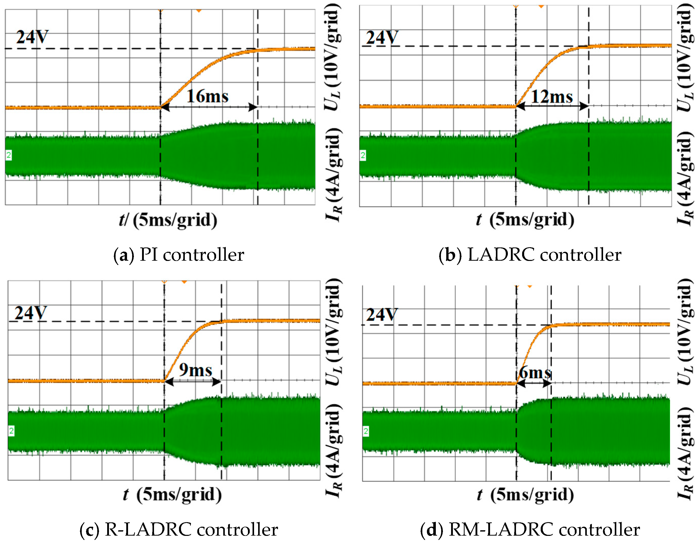
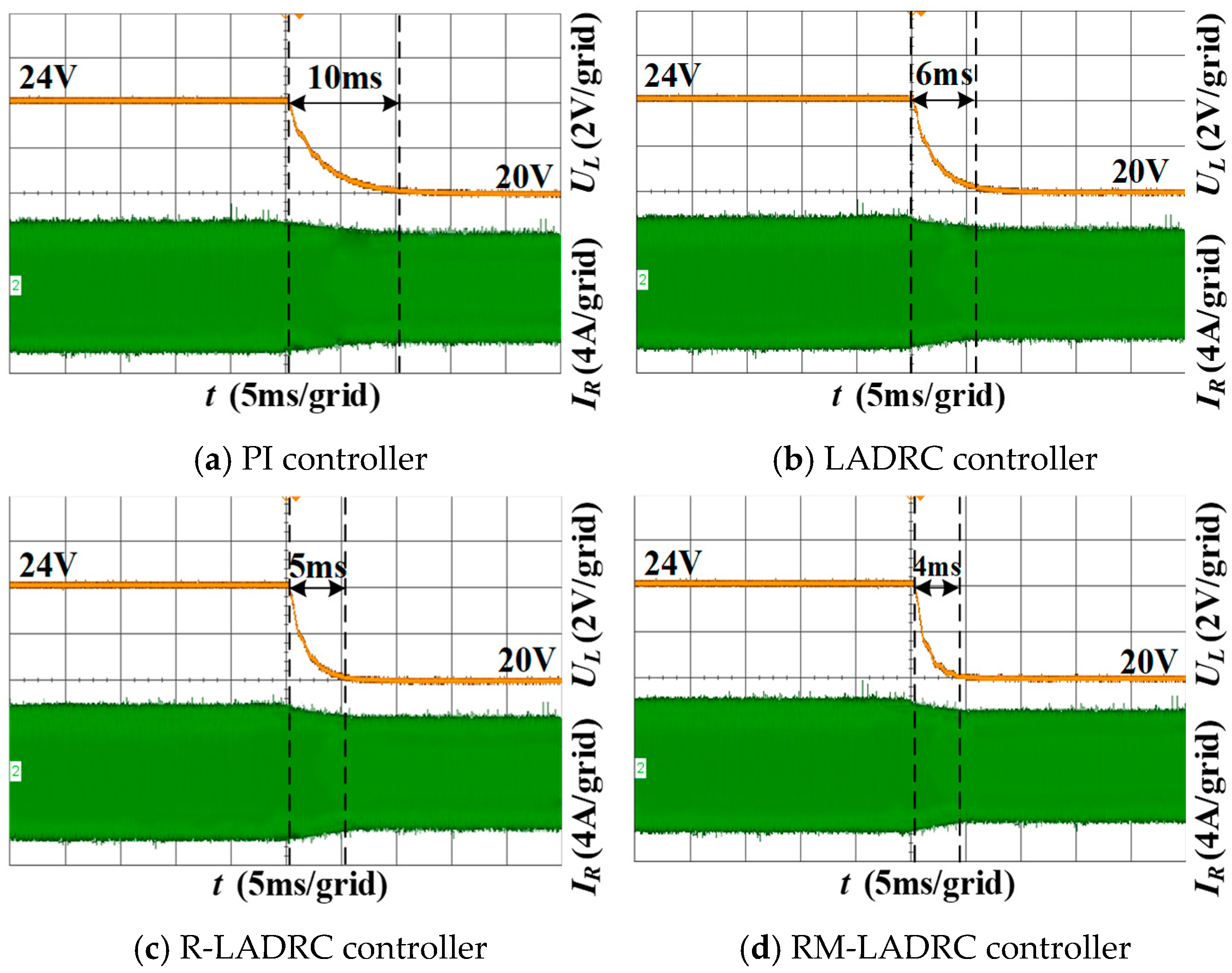
4.2.1. Closed-Loop Voltage-Controlled Startup Experiment
A comparative evaluation of closed-loop startup performance was conducted for the PI, LADRC, R-LADRC, and RM-LADRC controllers. The test scenario involved a step reference voltage transition from 0 V to 24 V with a constant load resistance of 3.2 Ω. Experimental waveforms capturing the voltage regulation dynamics during system initialization are comparatively presented in
Figure 11.
As evidenced by
Figure 11, all four controllers successfully eliminated output voltage overshoot. The PI controller required approximately 16 ms to reach a steady state, while LADRC, R-LADRC, and RM-LADRC achieved stabilization in 12 ms, 9 ms, and 6 ms, respectively. This comparative analysis conclusively demonstrates that the RM-LADRC exhibits superior dynamic response characteristics during closed-loop startup transients, attaining the reference voltage 33% faster than conventional LADRC and 62.5% quicker than baseline PI controller.
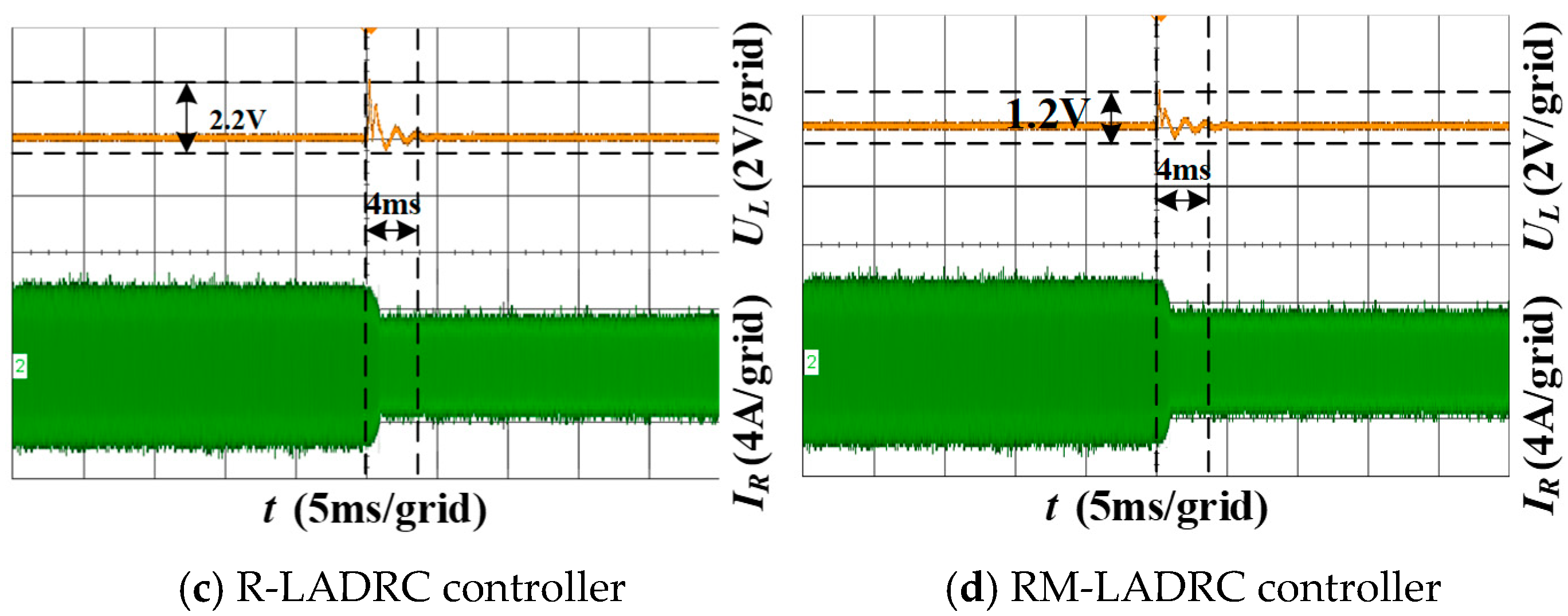
4.2.2. Load Step Experiment
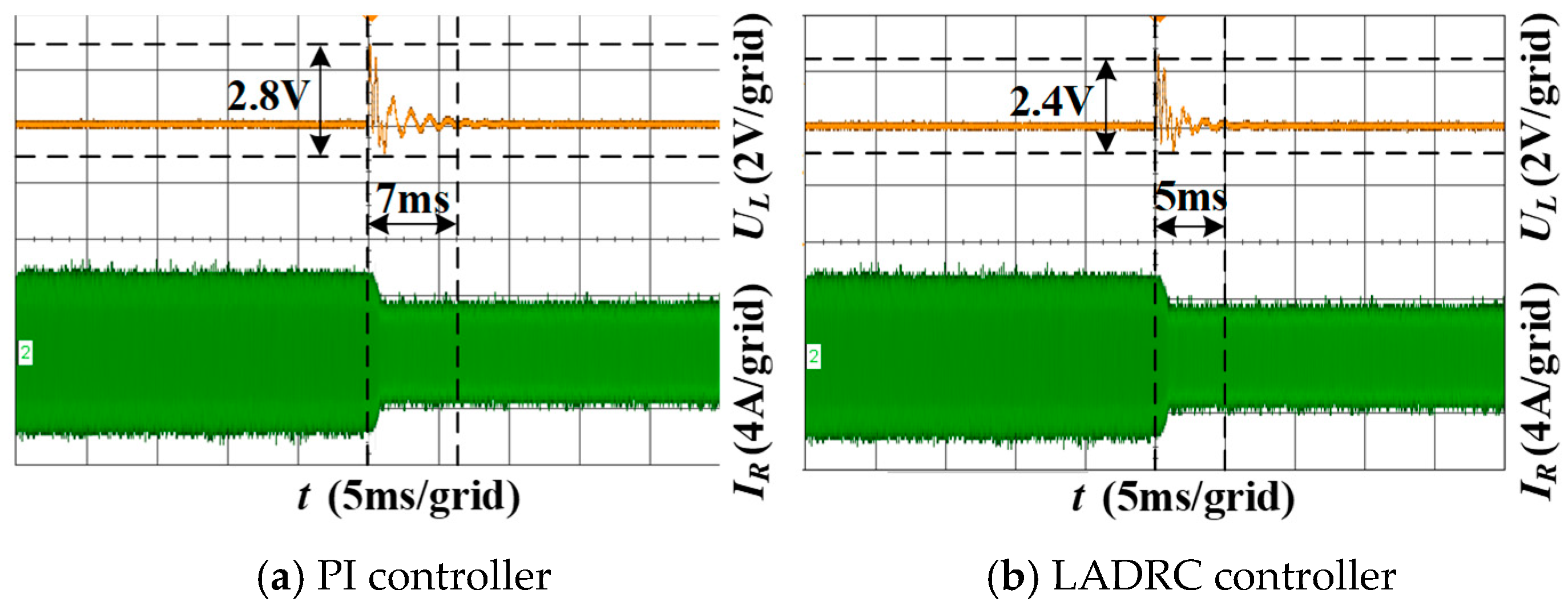
Figure 12 presents the load step response waveforms of different controllers. The experiment was configured with the Zeta converter’s reference voltage set to 24 V, while the electronic load resistance was switched from 3.2 Ω to 6.4 Ω.
As shown in
Figure 12, under the load step-change condition, the PI controller exhibits a settling time of 7 ms, with a voltage fluctuation range of 2.8 V. The LADRC achieves a settling time of 5 ms and a voltage fluctuation range of 2.4 V. In comparison, the R-LADRC further reduces the settling time to 4 ms, with a voltage fluctuation range of 2.2 V. Notably, the proposed RM-LADRC demonstrates a settling time of 4 ms and significantly suppresses the voltage fluctuation range to 1.2 V. Compared to the PI controller, the RM-LADRC shortens the settling time by 3 ms and reduces the voltage fluctuation range by 1.6 V, confirming its superior load disturbance rejection capability.
4.2.3. Reference Voltage Step Experiment
Figure 13 comparatively illustrates the reference voltage step-change responses of different controllers. During the experiment, the reference voltage was abruptly changed from 24 V to 20 V under a constant electronic load resistance of 3.2 Ω. The output voltage waveforms of all four controllers were systematically recorded to evaluate their dynamic regulation characteristics under this transient condition.
As evidenced in
Figure 13, all four controllers exhibit no overshoot during the reference voltage step-change. The PI controller requires 10 ms to settle to the reference value, while the LADRC, R-LADRC, and the proposed RM-LADRC achieve stabilization in 6 ms, 5 ms, and 4 ms, respectively. These experimental results demonstrate that the RM-LADRC achieves the shortest settling time under reference voltage transients, outperforming both the PI controller and other LADRC variants, thereby validating its superior dynamic response performance.
Based on the comprehensive analysis under three experimental conditions—closed-loop startup, load step change, and reference voltage step change—the proposed controller in this study demonstrates rapid and precise voltage regulation capability for the IPT system. Compared with PI controllers and other LADRC controllers, the RM-LADRC exhibits significantly improved response speed, which verifies its enhanced disturbance observation performance. Notably, this control strategy requires only two tuning parameters, making it more practical for engineering implementation.
4.2.4. System Transfer Efficiency Analysis
The system transmission efficiency is defined as the ratio of the output power from the Zeta converter to the input power of the Buck converter.
Figure 14 illustrates the relationship between the system transmission efficiency and load resistance
.
As shown in
Figure 14, under open-loop conditions (without composite control), with reference output voltages set at 24 V for the Zeta converter and 35 V for the Buck converter, the system transmission efficiency exhibits significant fluctuations across the load variation range of 3.2 Ω to 100 Ω. The average transmission efficiency measures only 72%, plummeting to 56% when
= 100 Ω. With the proposed composite control strategy, the system achieves substantial efficiency improvement—the average transmission efficiency rises to 84% while maintaining 80% efficiency even at
= 100 Ω.
The theoretical ceiling of transmission efficiency is determined by the sequential product of three constituent efficiencies; the power conversion efficiency of the Buck converter stage multiplied by the operational efficiency of the Zeta converter stage, further multiplied by the idealized (loss-neglected) energy transfer efficiency between the inverter and rectifier modules. This multiplicative relationship establishes the fundamental efficiency limit for the complete power transfer chain.
4.2.5. Comparison with Existing Literature
The proposed composite control method in this paper is compared with methods presented in other literature, as shown in
Table 3. In [
10], constant voltage control is achieved on the primary side based on the FSBB circuit. Although a feedforward + PI control strategy is employed, the improvement in settling time is limited due to the complexity of the IPT system and issues such as communication delays. In [
13], incorporating a state observer enhances the active disturbance rejection controller. However, the state observer introduces delays, resulting in minimal improvement in dynamic response. In [
14], combining feedforward compensation and non-smooth suppression strategies with an extended state observer improves the dynamic response speed. However, the method involves up to four tuning parameters, complicating its practical implementation. In [
15], maximum efficiency tracking is achieved through phase-shift control. The average transmission efficiency is relatively high since there is no cascaded DC-DC circuit on the primary side. Constant voltage control is implemented on the secondary side using a PID controller. However, the settling time is prolonged due to the inherent trade-off between speed and stability in PID control.
The advantage of the proposed method in this paper lies in its full utilization of model information to achieve constant voltage control on the secondary side based on the Zeta circuit, thereby enhancing the continual voltage control capability of the IPT system. Simultaneously, maximum efficiency tracking is realized on the primary side, ensuring the high-efficiency operation of the IPT system. In comparison, the proposed composite control method guarantees the high-efficiency operation of the IPT system and achieves a shorter settling time. Moreover, it involves only two tuning parameters, making it more conducive to practical engineering implementation.


