

Enhanced Charge Pump Architecture with Feedback Supply Selector for Optimized Switching Performance

 ,
,  and
and
Abstract
1. Introduction
2. Design and Implementation
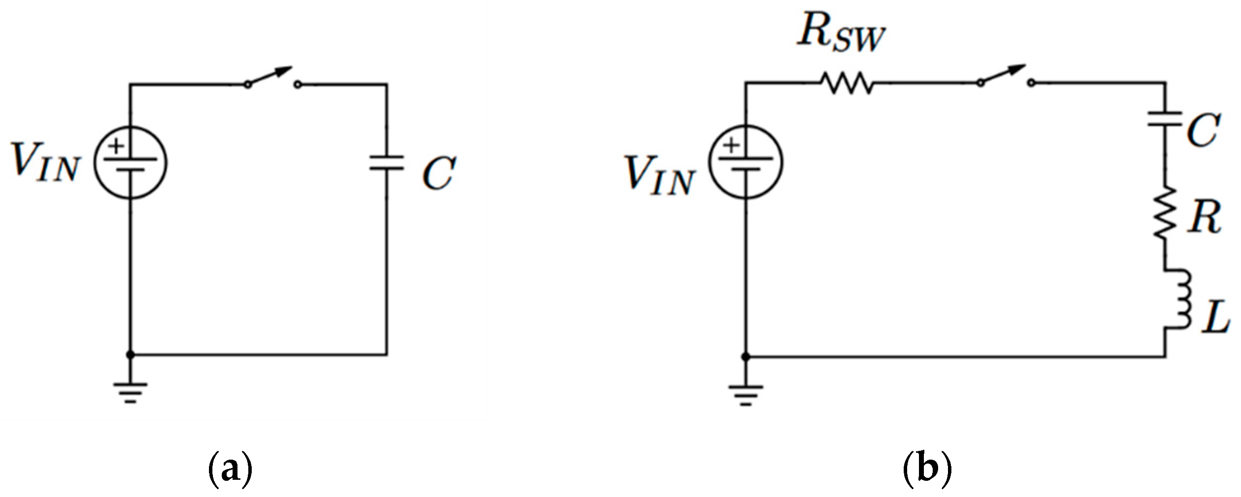
2.1. Charge Pump Principle
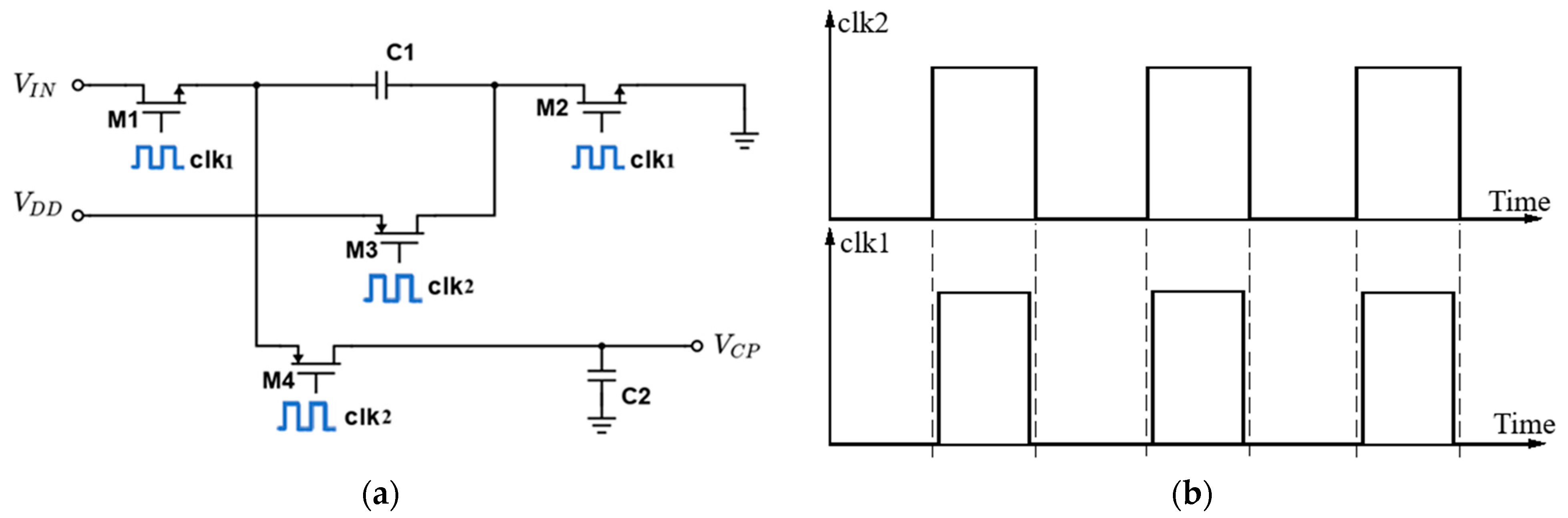
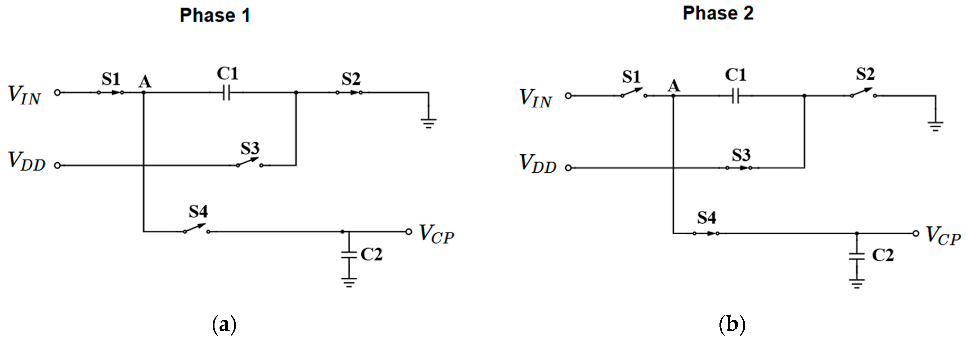
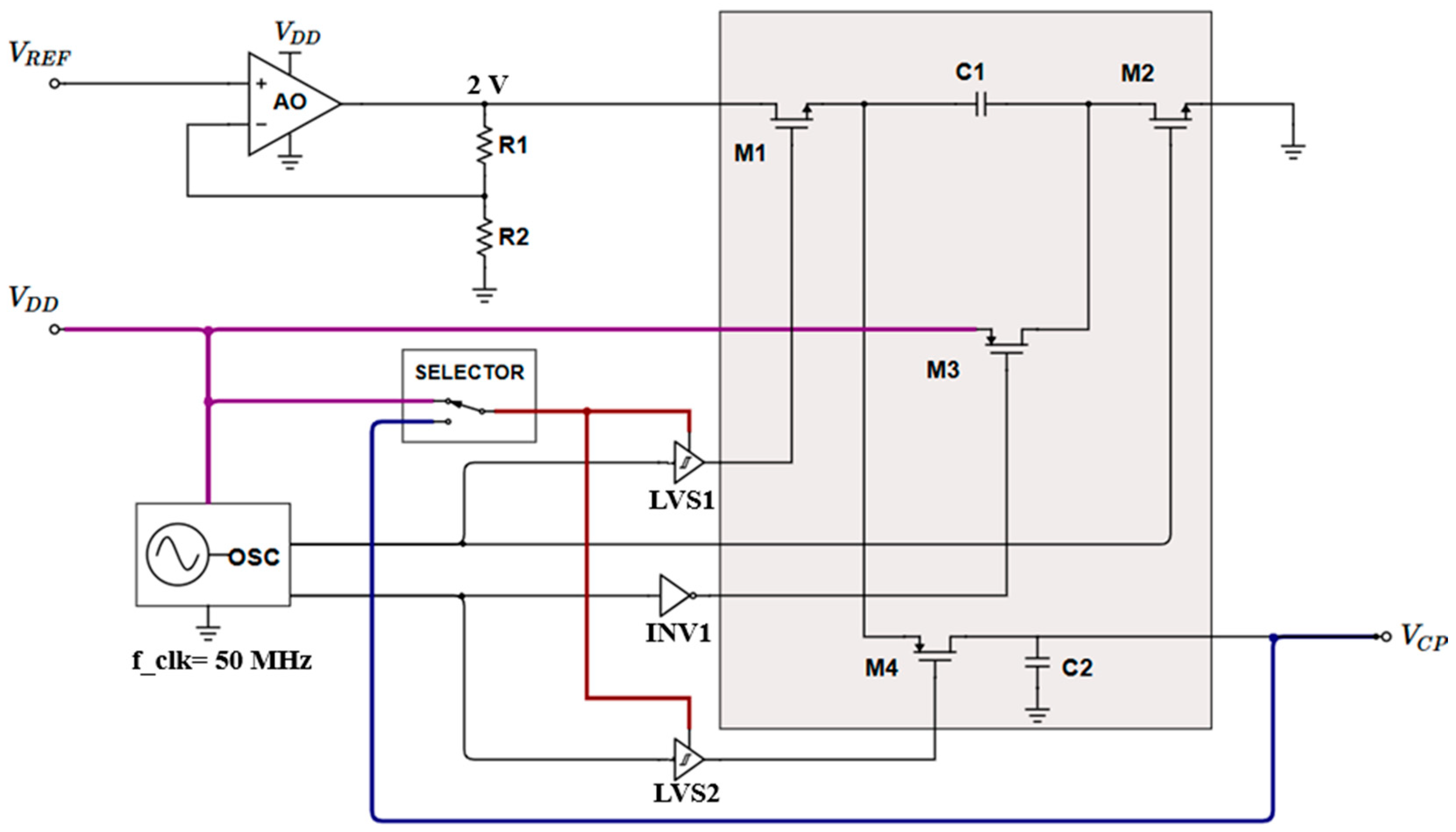
2.2. Proposed Switched-Capacitor Charge Pump
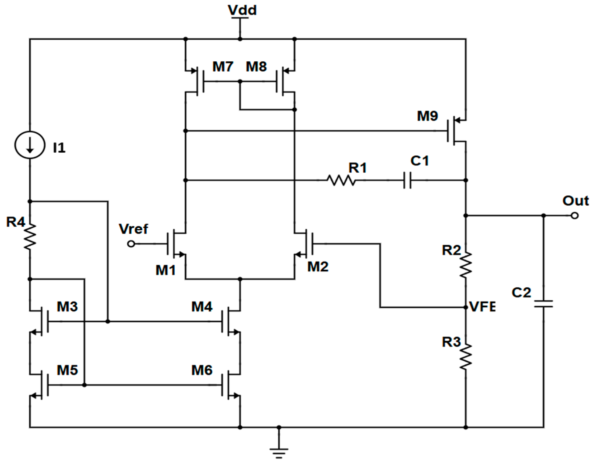
2.3. Low-Dropout Regulator (LDO)
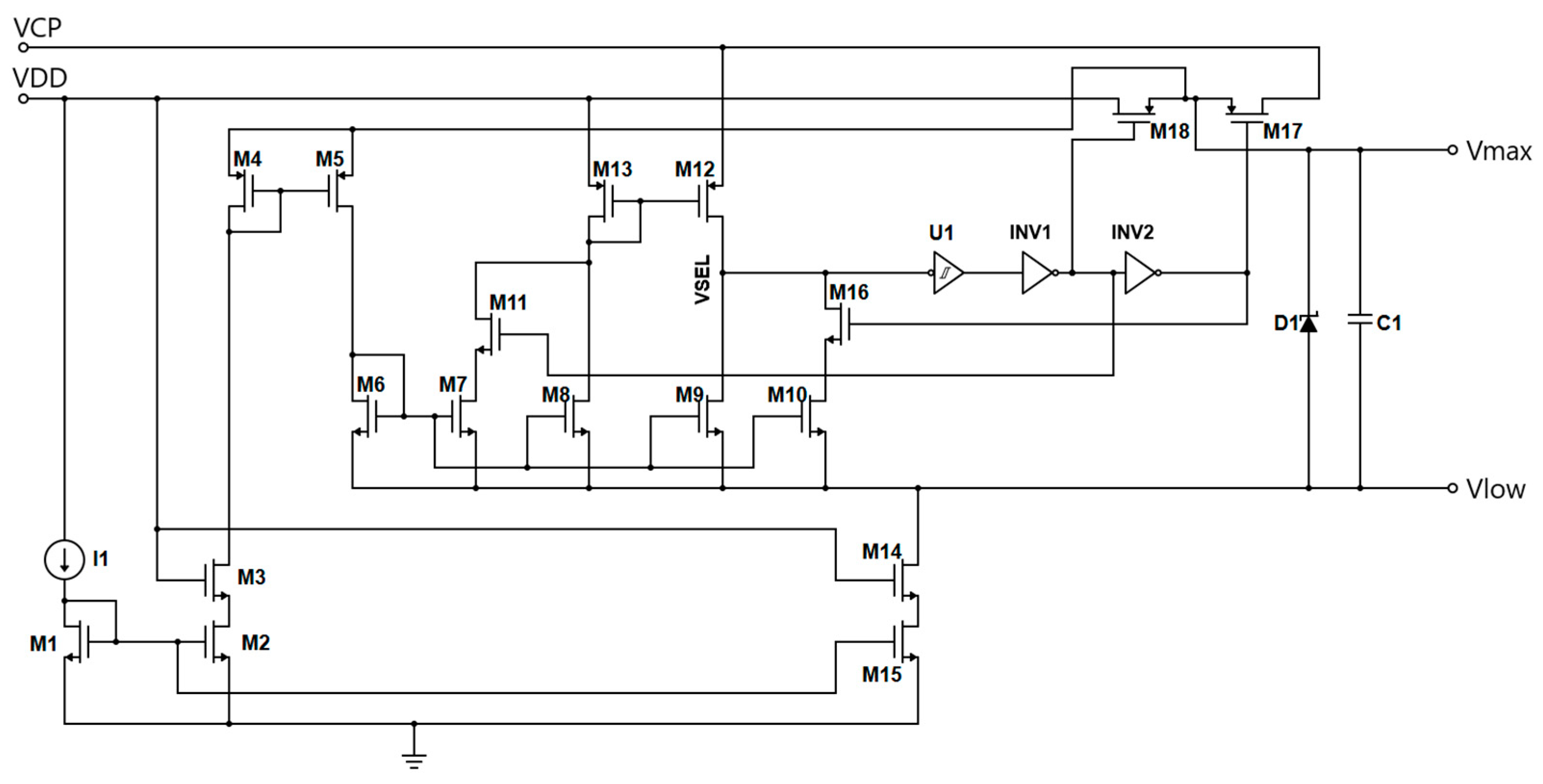
2.4. Innovative Supply Selector Circuit
2.5. Top-Level View of the Proposed Charge Pump
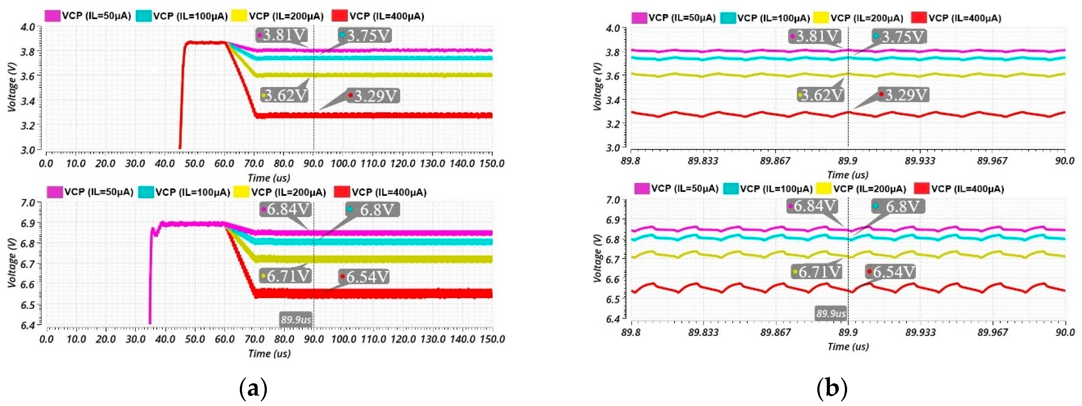
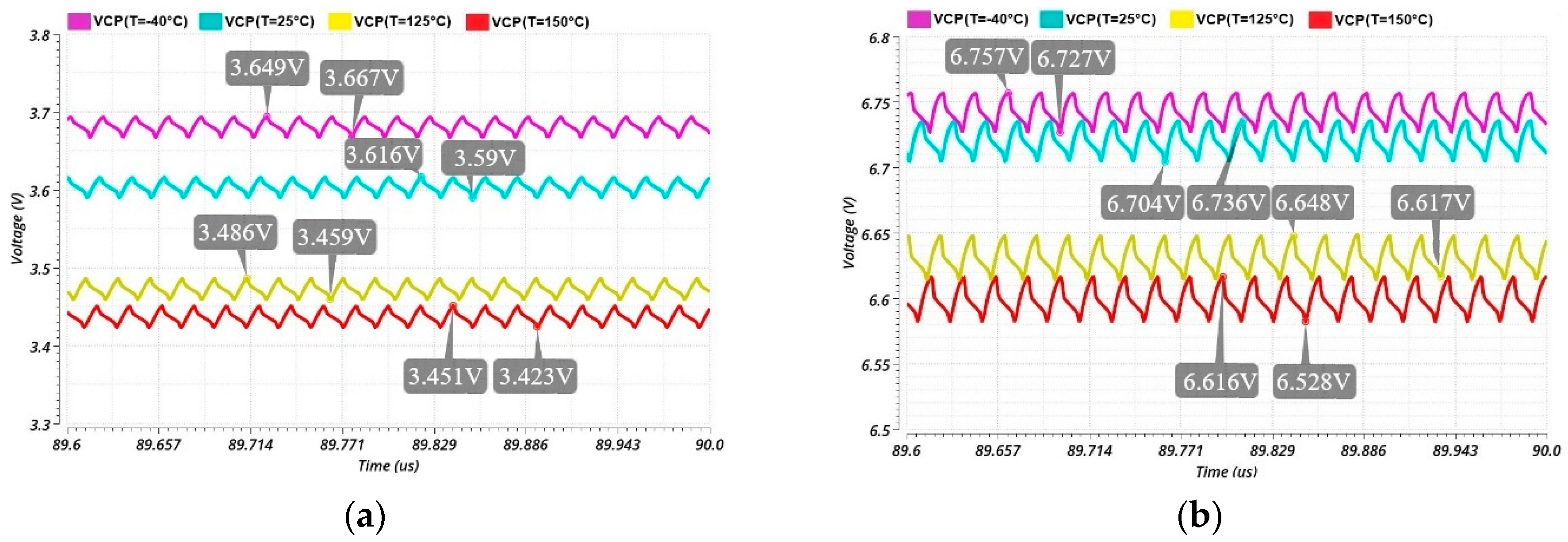
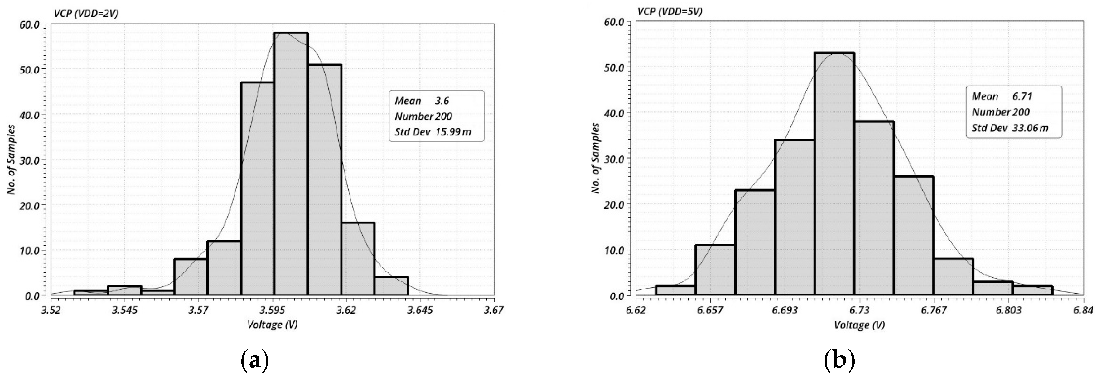
3. Simulations and Results
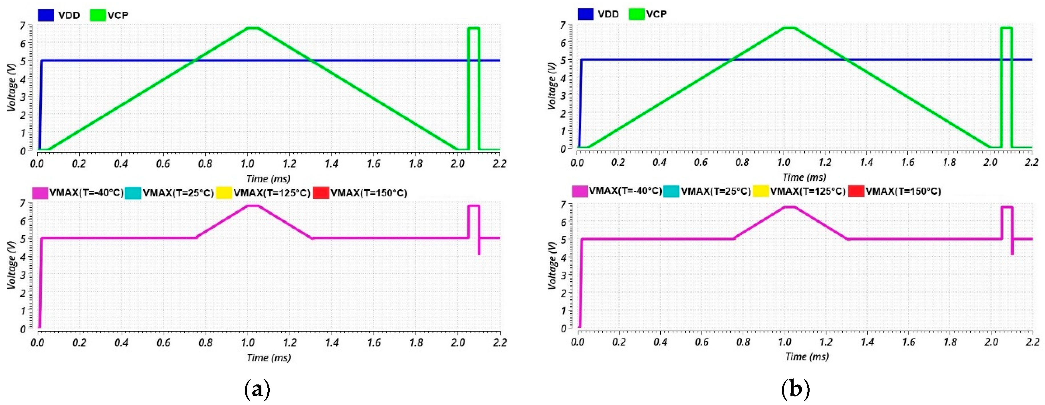
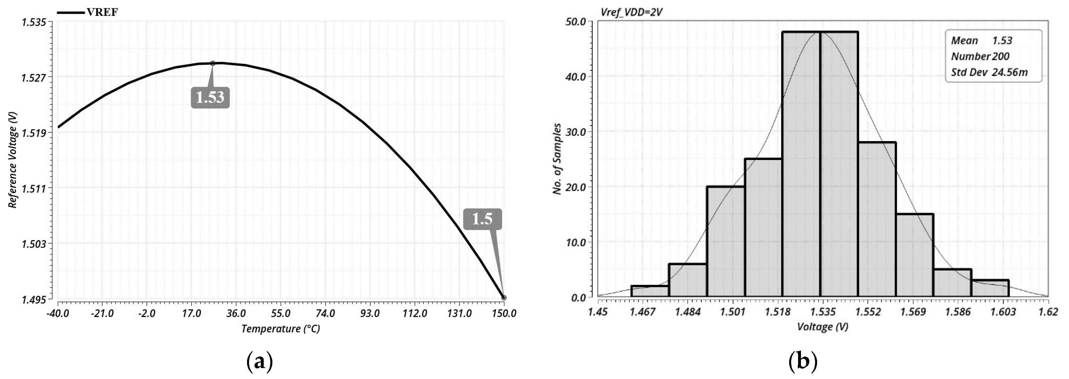
3.1. Schematic Level Simulations
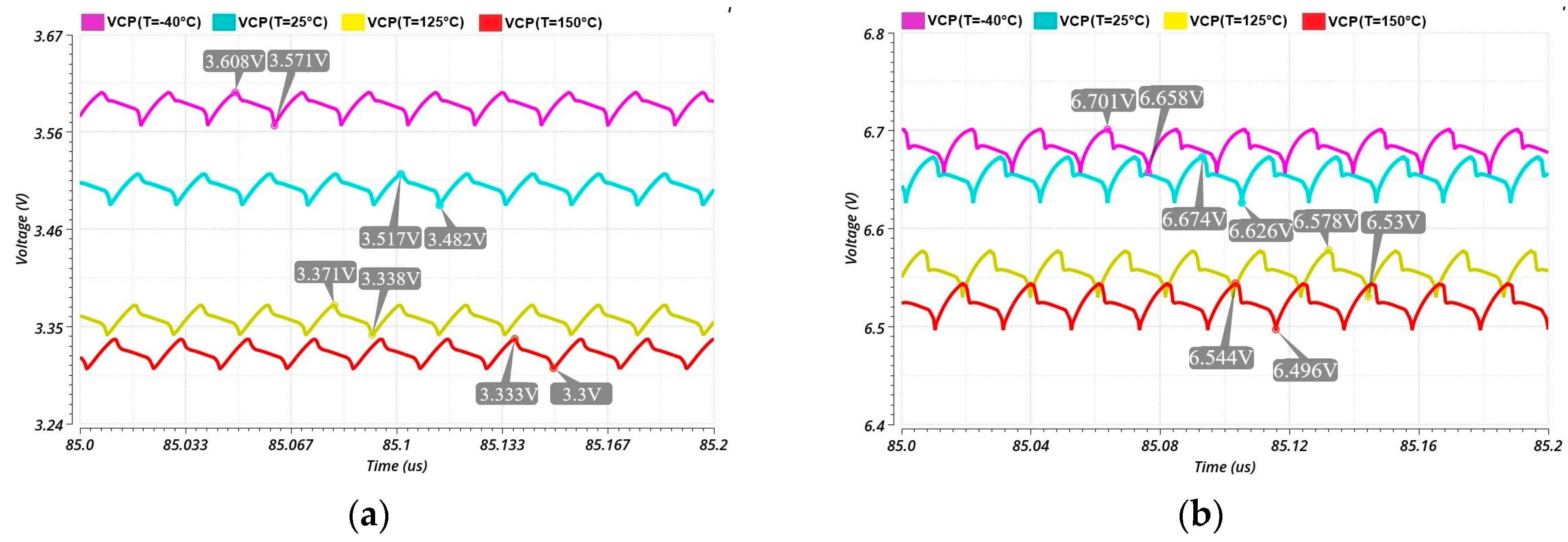
3.2. Post-Layout Simulations
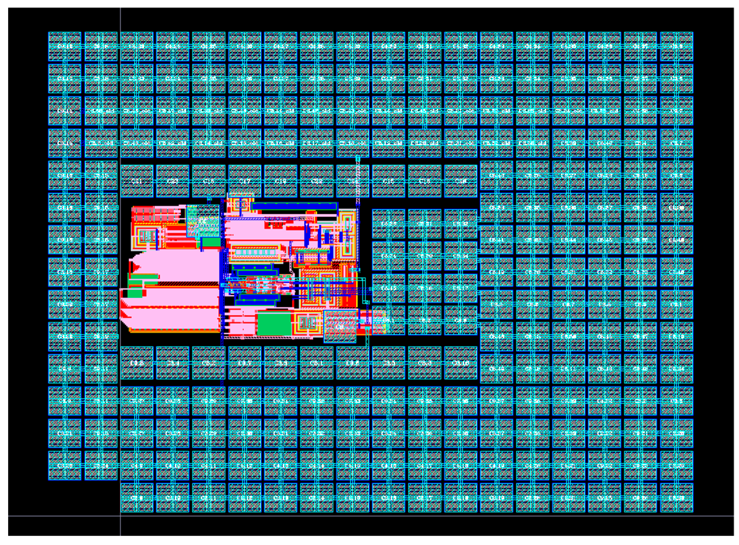
4. Layout Implementation
5. Conclusions
Author Contributions
Funding
Data Availability Statement
Conflicts of Interest
References
- Xie, L. Two-stage operational amplifier with Class A and B output stage. In Proceedings of the 2021 3rd International Academic Exchange Conference on Science and Technology Innovation (IAECST), Guangzhou, China, 10–12 December 2021; pp. 260–263. [Google Scholar] [CrossRef]
- Kumar, V.A.; Mohamed Asan Basiri, M. “Flexible and High Throughput Designs of 4-Stage Operational Amplifier. In Proceedings of the 2024 15th International Conference on Computing Communication and Networking Technologies (ICCCNT), Kamand, India, 14–16 March 2024; pp. 1–6. [Google Scholar] [CrossRef]
- Cancelli, R.; Avitabile, G.; Florio, A. Designing and Optimizing a 2.4 GHz Complementary Metal–Oxide-Semiconductor Class-E Power Amplifier Combining Standard and High-Voltage Metal–Oxide-Semiconductor Field-Effect Transistors. Electronics 2025, 14, 1135. [Google Scholar] [CrossRef]
- Stancu, C.; Neacsu, A.; Ionescu, T.; Stanescu, C.; Profirescu, O.; Dobrescu, D.; Dobrescu, L. Offset Voltage Reduction in Two-Stage Folded-Cascode Operational Amplifier Using High-Precision Source Degeneration. Electronics 2023, 12, 4534. [Google Scholar] [CrossRef]
- Chaya, N.; Ghosh, A.; Srinivas, B.; Jain, A. An Ultra Low Power Low noise Operational Transconductance Amplifier for Biomedical Front-end Applications. In Proceedings of the 2020 International Conference on Inventive Computation Technologies (ICICT), Coimbatore, India, 26–28 February 2020; pp. 1020–1023. [Google Scholar] [CrossRef]
- Tai, F.; Nie, Z.; Wang, Y.; Chao, X.; Li, Q. A Low-Noise and Settling-Enhanced Switched-Capacitor Amplifier with Correlated Level Shifting and Bandwidth Switching. In Proceedings of the 2023 IEEE International Symposium on Circuits and Systems (ISCAS), Monterey, CA, USA, 21–25 May 2023; pp. 1–4. [Google Scholar] [CrossRef]
- Hoentschel, J.; Wei, A. From the present to the future: Scaling of planar VLSI-CMOS devices towards 3D-FinFETs and beyond 10 nm CMOS technologies; manufacturing challenges and future technology concepts. In Proceedings of the 2015 China Semiconductor Technology International Conference, Shanghai, China, 15–16 March 2015; pp. 1–4. [Google Scholar] [CrossRef]
- Kouhalvandi, L.; Aygün, S.; Güneş, E.O.; Kırcı, M. An improved 2 stage opamp with rail-to-rai! gain-boosted folded cascode input stage and monticelli rail-to-rail class AB output stage. In Proceedings of the 2017 24th IEEE International Conference on Electronics, Circuits and Systems (ICECS), Batumi, Georgia, 5–8 December 2017; pp. 542–545. [Google Scholar] [CrossRef]
- Gagliardi, F.; Catania, A.; Piotto, M.; Bruschi, P.; Dei, M. A Novel High-Performance Parallel-Type Slew-Rate Enhancer for LCD-Driving Applications. In Proceedings of the 2023 18th Conference on Ph.D Research in Microelectronics and Electronics (PRIME), Valencia, Spain, 18–21 June 2023; pp. 65–68. [Google Scholar] [CrossRef]
- Shuai, H.E.; Guo, Z.; Zheng, X.; Chen, H.; Li, Q. Research on Low Power Constant Transconductance Rail-to-Rail Operational Amplifier Technology. In Proceedings of the 2020 IEEE 15th International Conference on Solid-State & Integrated Circuit Technology (ICSICT), Kunming, China, 3–6 November 2020; pp. 1–3. [Google Scholar] [CrossRef]
- Rehani, A.; Chaitanya, G.V.; Anantula, P. A High Area and Current Efficient Charge Pump Design. In Proceedings of the 2024 International Conference on Microelectronics (ICM), Doha, Qatar, 14–17 December 2024; pp. 1–5. [Google Scholar] [CrossRef]
- Ng, W.-K.; Ertugrul, N.; Tam, W.-S.; Kok, C.-W. Design Strategy for 2-phase Switched Capacitor Charge Pump. In Proceedings of the 2021 31st Australasian Universities Power Engineering Conference (AUPEC), Perth, Australia, 26–30 September 2021; pp. 1–6. [Google Scholar] [CrossRef]
- Chowdhury, S.; Gurpinar, E.; Ozpineci, B. Capacitor Technologies: Characterization, Selection, and Packaging for Next-Generation Power Electronics Applications. IEEE Trans. Transp. Electrif. 2022, 8, 2710–2720. [Google Scholar] [CrossRef]
- Yim, T.; Lee, C.; Yoon, H. A High Speed Modified Dickson Charge Pump. In Proceedings of the 2021 IEEE International Symposium on Circuits and Systems (ISCAS), Daegu, Republic of Korea, 22–28 May 2021; pp. 1–5. [Google Scholar] [CrossRef]
- Rajora, R.; Sharma, K. Design and analysis of a low-power, high-efficiency 4-stage Dickson charge pump using CNTFETs. In Proceedings of the 2023 Second International Conference on Trends in Electrical, Electronics, and Computer Engineering (TEECCON), Bangalore, India, 23–24 August 2023; pp. 406–410. [Google Scholar] [CrossRef]
- Ballo, A.; Grasso, A.D.; Palumbo, G. Signal Amplification by Means of a Dickson Charge Pump: Analysis and Experimental Validation. Chips 2022, 1, 72–82. [Google Scholar] [CrossRef]
- Hussein, S.H.; Yaseen, M.T. Performance Evaluation of Low-Voltage CMOS Switched-Capacitor Circuit. In Proceedings of the 2021 8th International Conference on Electrical and Electronics Engineering (ICEEE), Antalya, Turkey, 9–11 April 2021; pp. 40–43. [Google Scholar] [CrossRef]
- Sahakyan, H.; Hayrapetyan, A.; Harutyunyan, S.; Stepanyan, A.; Azatyan, H.; Hovsepyan, G. A Low Dropout Voltage Regulator with Higher Than Supply Output Voltage and Load Based Frequency Control System. In Proceedings of the 2020 IEEE 40th International Conference on Electronics and Nanotechnology (ELNANO), Kyiv, Ukraine, 22–24 April 2020; pp. 366–369. [Google Scholar] [CrossRef]
- Ren, B.; Zhan, C.; Liu, F. A 0.8-V-VIN 3.76-nW 23.1-ppm/°C Low Dropout Regulator Based on Flipped Voltage Follower with Embedded CMOS Voltage Reference. In Proceedings of the 2024 IEEE International Conference on Integrated Circuits, Technologies and Applications (ICTA), Hangzhou, China, 25–27 October 2024; pp. 192–193. [Google Scholar] [CrossRef]
- Li, Y.; Li, Z.; Qian, L.; Wang, X.; Zhu, Z. A Low Quiescent Current Fast Transient LDO Regulator with Segmented Pass Transistors. IEEE Trans. Circuits Syst. II Express Briefs 2025, 72, 13–17. [Google Scholar] [CrossRef]
- Stanescu, C.; Dinca, C.; Iacob, R. Soft-start low voltage CMOS LDO. In Proceedings of the CAS 2013 (International Semiconductor Conference), Sinaia, Romania, 14–16 October 2013; pp. 185–188. [Google Scholar] [CrossRef]
- Shah, M.K.; Gaidhane, V.H.; Prasannan, C. Stability Analysis of Two-Stage OTA with Frequency Compensation. In Proceedings of the 2021 IEEE International IOT, Electronics and Mechatronics Conference (IEMTRONICS), Toronto, ON, Canada, 21–24 April 2021; pp. 1–6. [Google Scholar] [CrossRef]
- Stancu, C.; Neacsu, A.; Profirescu, O.; Dobrescu, D.; Dobrescu, L. Temperature and Power Supply Compensated CMOS Clock Circuit Based on Ring Oscillator. Electronics 2023, 12, 507. [Google Scholar] [CrossRef]
- Olaru, D.; Floricău, D. Optimal Method for Controlled Switching Circuits. UPB Sci. Bull. Ser. C 2009, 71, 187–196. [Google Scholar]
- Kar, G.C.; Sawan, M. Low-power high-voltage charge pumps for implantable microstimulators. In Proceedings of the 2012 IEEE International Symposium on Circuits and Systems (ISCAS), Seoul, Republic of Korea, 20–23 May 2012; pp. 2247–2250. [Google Scholar] [CrossRef]
- Jiang, X.; Yu, X.; Moez, K.; Elliott, D.G.; Chen, J. High-Efficiency Charge Pumps for Low-Power On-Chip Applications. IEEE Trans. Circuits Syst. I Regul. Pap. 2018, 65, 1143–1153. [Google Scholar] [CrossRef]
- Ballo, A.; Grasso, A.D.; Palumbo, G. A High-Performance Charge Pump Topology for Very-Low-Voltage Applications. IEEE Trans. Circuits Syst. II Express Briefs 2020, 67, 1304–1308. [Google Scholar] [CrossRef]
- Ballo, A.; Grasso, A.D.; Palumbo, G. Charge Pump Improvement for Energy Harvesting Applications by Node Pre-Charging. IEEE Trans. Circuits Syst. II Express Briefs 2020, 67, 3312–3316. [Google Scholar] [CrossRef]
- Jacob Baker, R. CMOS Circuit Design, Layout, and Simulation, 3rd ed.; John Wiley & Sons, Inc.: Hoboken, NJ, USA, 2010. [Google Scholar]
- Hastings, A. The Art of Analog Layout, 1st ed.; Prentice Hall: Hoboken, NJ, USA, 2001. [Google Scholar]
- Razavi, B. Design of Analog CMOS Integrated Circuits, 2nd ed.; McGraw-Hill Education: New York, NY, USA, 2016. [Google Scholar]


| Parameter | Value |
|---|---|
| (W/L) M1–M2 | 20/2 µm/µm |
| (W/L) M3, M4 | 12/2, 60/2 µm/µm |
| (W/L) M5, M6 | 12/2, 60/2 µm/µm |
| (W/L) M7–M8 | 40/0.5 µm/µm |
| (W/L) M9 | 800/0.5 µm/µm |
| R1 | 28.9 kΩ |
| R2 | 200 kΩ |
| R3 | 600 kΩ |
| R4 | 200 kΩ |
| C1 | 1.15 pF |
| I1 | 1 µA |
| Parameter | Value |
|---|---|
| (W/L) M1–M2, M15 | 8/4, 96/4 µm/µm |
| (W/L) M3, M14 | 12/1, 144/1 µm/µm |
| (W/L) M4–M5 | 18/3 µm/µm |
| (W/L) M6–M7, M10 | 4/4 µm/µm |
| (W/L) M8–M9 | 8/4 µm/µm |
| (W/L) M11, M16 | 10/0.5 µm/µm |
| (W/L) M12–M13 | 6/3 µm/µm |
| (W/L) M17–M18 | 20/0.5 µm/µm |
| (W/L) M5–M6, M9–M10 | 480/10, 416/3 µm/µm |
| (W/L) D1 | 0.8/5.4 µm/µm |
| C1 | 900 fF |
| I1 | 1µA |
| Parameter | VDD = 2 V | VDD = 5 V |
|---|---|---|
| Input voltage (V) | 2 | 5 |
| Output voltage (V) (ILOAD = 200 µA) | 3.6 | 6.71 |
| Load capacitance (pF) | 160 | 160 |
| Number of stages | 1 | 1 |
| Clock frequency | 50 MHz | 50 MHz |
| Maximum output current | 400 µA | 400 µA |
| Output voltage ripple (mV) (ILOAD= 200 µA) | 26 | 32 |
| Output current (no load) (µA) | 354.8 | 628.4 |
| Parameter | VDD = 2 V | VDD = 5 V | Schematic Level VDD = 2 V | Schematic Level VDD = 5 V |
|---|---|---|---|---|
| Input voltage (V) | 2 | 5 | 2 | 5 |
| Output voltage (V) (ILOAD = 200 µA) | 3.503 | 6.65 | 3.6 | 6.71 |
| Load capacitance (pF) | 160 | 160 | 160 | 160 |
| Number of stages | 1 | 1 | 1 | 1 |
| Clock frequency | 48.12 MHz | 48.13 MHz | 50 MHz | 50 MHz |
| Maximum output current | 400 µA | 400 µA | 400 µA | 400 µA |
| Output voltage ripple (mV) (ILOAD = 200 µA) | 35 | 48 | 26 | 32 |
| Output current (no load) (µA) | 352.6 | 625.1 | 354.8 | 628.4 |
| Parameter | [25] | [26] | [27] | [28] | This Work |
|---|---|---|---|---|---|
| Year | 2012 | 2018 | 2020 | 2020 | 2025 |
| Technology (CMOS) | 130 nm | 130 nm | 65 nm | 65 nm | 250 nm |
| Input voltage (V) | N/A | 1.2 | 0.4 | 0.4 | 2 |
| Output voltage (V) | 10 | 7.45 | 1.9 | 2 | 3.505 |
| Load capacitance (pF) | 1 µF | N/A | 160 | 160 | 160 |
| Number of stages | N/A | 8 | 4 | 4 | 1 |
| Voltage gain per stage | N/A | 6.20 | 1.476 | 1.49 | 1.5 |
| Clock frequency | 0.1 MHz | N/A | 25 | 4 | 48.12 MHz |
| Maximum output current | 500 µA | 5 mA | N/A | N/A | 400 µA |
| Output voltage ripple (mV) (with ILOAD) | 100 | 73 | 100 | N/A | 35 |
| Output current (no load) (µA) | 250 | N/A | 30 | 12.6 | 352.6 |
| Power consumption (no load) (µW) | 897.6 | 37250 | 12 | 5.04 | 705.2 |
| Die area (mm2) | 2.25 | N/A | 0.031 | 0.021 | 0.35 |
Disclaimer/Publisher’s Note: The statements, opinions and data contained in all publications are solely those of the individual author(s) and contributor(s) and not of MDPI and/or the editor(s). MDPI and/or the editor(s) disclaim responsibility for any injury to people or property resulting from any ideas, methods, instructions or products referred to in the content. |
© 2025 by the authors. Licensee MDPI, Basel, Switzerland. This article is an open access article distributed under the terms and conditions of the Creative Commons Attribution (CC BY) license (https://creativecommons.org/licenses/by/4.0/).
Share and Cite
Stancu, C.; Mitu, A.A.; Ionescu, T.; Neacsu, A.; Dobrescu, L.; Dobrescu, D. Enhanced Charge Pump Architecture with Feedback Supply Selector for Optimized Switching Performance. Electronics 2025, 14, 1484. https://doi.org/10.3390/electronics14071484
Stancu C, Mitu AA, Ionescu T, Neacsu A, Dobrescu L, Dobrescu D. Enhanced Charge Pump Architecture with Feedback Supply Selector for Optimized Switching Performance. Electronics. 2025; 14(7):1484. https://doi.org/10.3390/electronics14071484
Chicago/Turabian StyleStancu, Cristian, Anca Andreea Mitu, Teodora Ionescu, Andrei Neacsu, Lidia Dobrescu, and Dragos Dobrescu. 2025. "Enhanced Charge Pump Architecture with Feedback Supply Selector for Optimized Switching Performance" Electronics 14, no. 7: 1484. https://doi.org/10.3390/electronics14071484
APA StyleStancu, C., Mitu, A. A., Ionescu, T., Neacsu, A., Dobrescu, L., & Dobrescu, D. (2025). Enhanced Charge Pump Architecture with Feedback Supply Selector for Optimized Switching Performance. Electronics, 14(7), 1484. https://doi.org/10.3390/electronics14071484