Article

Three-Channel Fully Integrated Galvanic Isolation Interface in GaN Technology

1
DIEEI, Università di Catania, I-95125 Catania, Italy
2
STMicroelectronics, I-95121 Catania, Italy
*
Author to whom correspondence should be addressed.
Electronics 2025, 14(7), 1403; https://doi.org/10.3390/electronics14071403
Submission received: 8 January 2025 / Revised: 7 March 2025 / Accepted: 24 March 2025 / Published: 31 March 2025
(This article belongs to the Special Issue Gallium Nitride (GaN)-Based Power Electronic Devices and Systems)

Abstract

:
This paper presents a three-channel galvanic isolation interface in GaN technology. Driver, diagnostic, and control channels have been implemented in a two-die integrated system to perform an isolation interface for a high-performance power switching system. Chip-to-chip communication has been used, which is based on planar micro-antennas with on–off keying modulated RF carriers. This approach provides a high isolation rating by properly setting the distance between chips. Various innovation aspects are adopted with respect to previously published works. They mainly involve the receiver robustness thanks to the switched-capacitor bias control, a bidirectional data channel implementation for power section diagnostic, and a duty cycle distortion compensation for accurate PWM signal. Driver and control channels use RF carriers of about 2 GHz and 0.9 GHz and achieve 2 MHz and 0.5 MHz measured pulse width modulation signals, respectively. The bidirectional channel adopts an RF carrier of about 400 MHz and exhibits a maximum measured data rate as high as 10 Mb/s. Thanks to the extensive use of switched-capacitor circuit solutions, well-controlled behavior is achieved against the large process tolerances and temperature drifts of the GaN technology. The isolation interface is supplied at 6 V and occupies a die area of 7.6 mm2 for each chip.

1. Introduction

Gallium Nitride (GaN) High-Electron-Mobility Transistor (HEMT) is a promising technology for next-generation smart power and RF systems thanks to its inherent material properties that give rise to devices with excellent figures of merit [1]. The wide bandgap and high electron mobility of the two-dimensional electron gas (2DEG) at the GaN/AlGaN interface allow transistors with a higher breakdown, faster switching speed, and lower on-resistance than silicon ones [2,3,4,5,6].
In recent years, the GaN technology has been improved, mainly to improve power conversion efficiency, thus achieving more mature technology. In addition, a lot of attention has been paid to low-voltage GaN devices that are mandatory for a fully integrated power system. The integration on the same substrate of low-voltage and high-voltage GaN transistors allows the switching frequency to be further increased. Indeed, the implementation of a driver and power switch in a two-device solution is affected by frequency limitations due to parasitic inductances [7,8,9,10]. Moreover, driver/power switch integration further increases power efficiency and compactness thanks to the high switching frequency mentioned before, which reduces the size of capacitors and inductors in the final power application. Unfortunately, control circuit design in GaN technology is a challenging task mainly due to the lack of p-channel transistors and the wide spread of transistor electrical parameters [11,12,13,14,15]. To overcome these limitations, several research efforts have been addressed to all-GaN design approaches for integrated basic cells, gate drivers, and power switch systems, including the control circuitry [16,17,18,19,20,21,22,23,24,25,26,27,28].
Many power switching systems for different application fields (medical, smart-home systems, electric vehicles, industrial instrumentations, etc.) need galvanic isolation to be compliant with safety and reliability standards [29,30,31]. Among several approaches for galvanic isolation, an effective and low-cost solution for isolation ratings higher than 10 kV is the near-field chip-to-chip communication, which uses integrated micro-antennas and a modulated RF carrier to transmit data through the isolation interface [32,33,34,35,36,37,38,39,40,41,42,43,44].
This paper presents a fully integrated three-channel galvanic isolation interface in a GaN technology, which is based on the chip-to-chip communication approach shown in Figure 1. The overall system is made up of two chips, a controller chip (chip CTR) and a power chip (chip PW). They should be assembled side-by-side in the package lead frames at a proper distance through isolation (DTI) to guarantee the desired galvanic isolation performance. Chip-to-chip wireless communication is achieved using magnetically coupled planar micro-antennas and OOK-modulated RF carriers.
Two works by the authors on galvanic isolation with chip-to-chip and magnetic micro-antennas were recently published [45,46]. In [45], silicon BCD technology is used whereas [46] uses a GaN technology. Although the two system architectures are similar, they greatly differ in the circuit design approaches. The galvanic isolation interface in [46] has two channels, i.e., a driver channel and a power supply control channel. The main challenge in the design of GaN mixed analog/digital integrated circuits is to overcome the strong technology limitations with a robust design approach. For this purpose, further work was carried out by the authors to improve previous circuit solutions, including additional system functionalities. Specifically, more robust and accurate circuits were arranged for the receiver and a duty cycle distortion compensation circuit was added. Moreover, a bidirectional diagnostic channel was implemented since it is important in some high-performance switching systems to guarantee circuit safety and reliable operation.
To increase the robustness of the receiver, the switched-capacitor (SC) approach was properly exploited to improve both offset compensation and amplification approaches. Specifically, a dedicated feedback loop was arranged for the offset compensation, and the traditional differential stage with resistive load was replaced by a high-gain SC amplifier with dynamic biasing. These approaches increased accuracy against process tolerances and temperature bias drift.
The paper is organized as follows. Section 2 deals with the three-channel system architecture. Section 3 presents the improved receiver along with a detailed comparison with the previous one. Section 5 describes measurements, and Section 6 presents the conclusions.

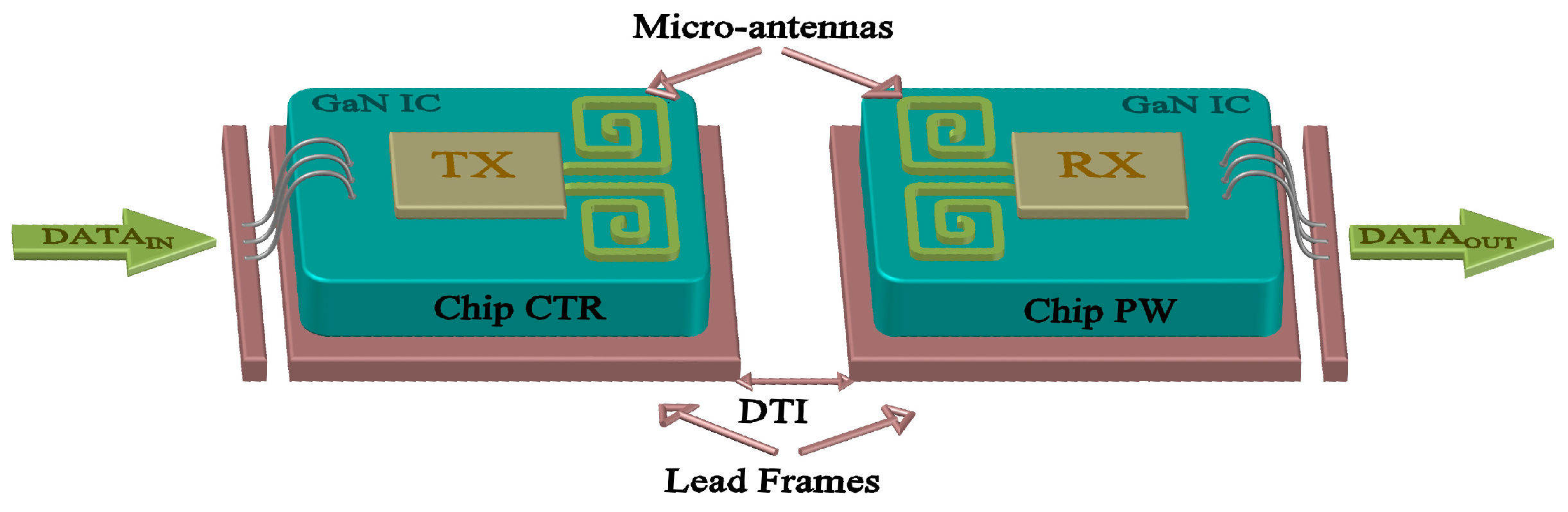
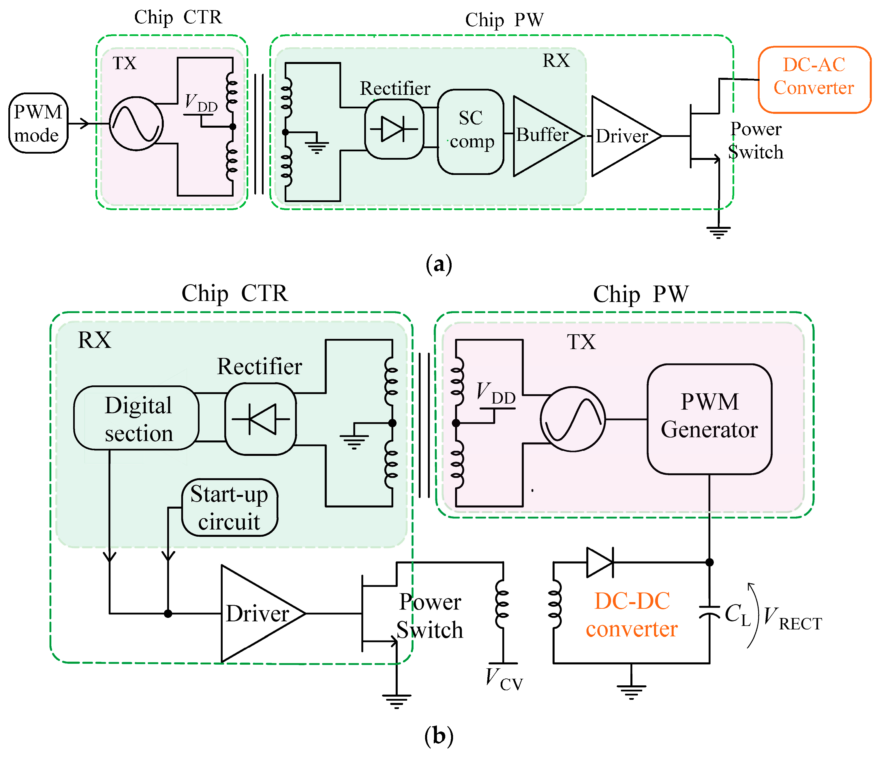
2. System Architecture
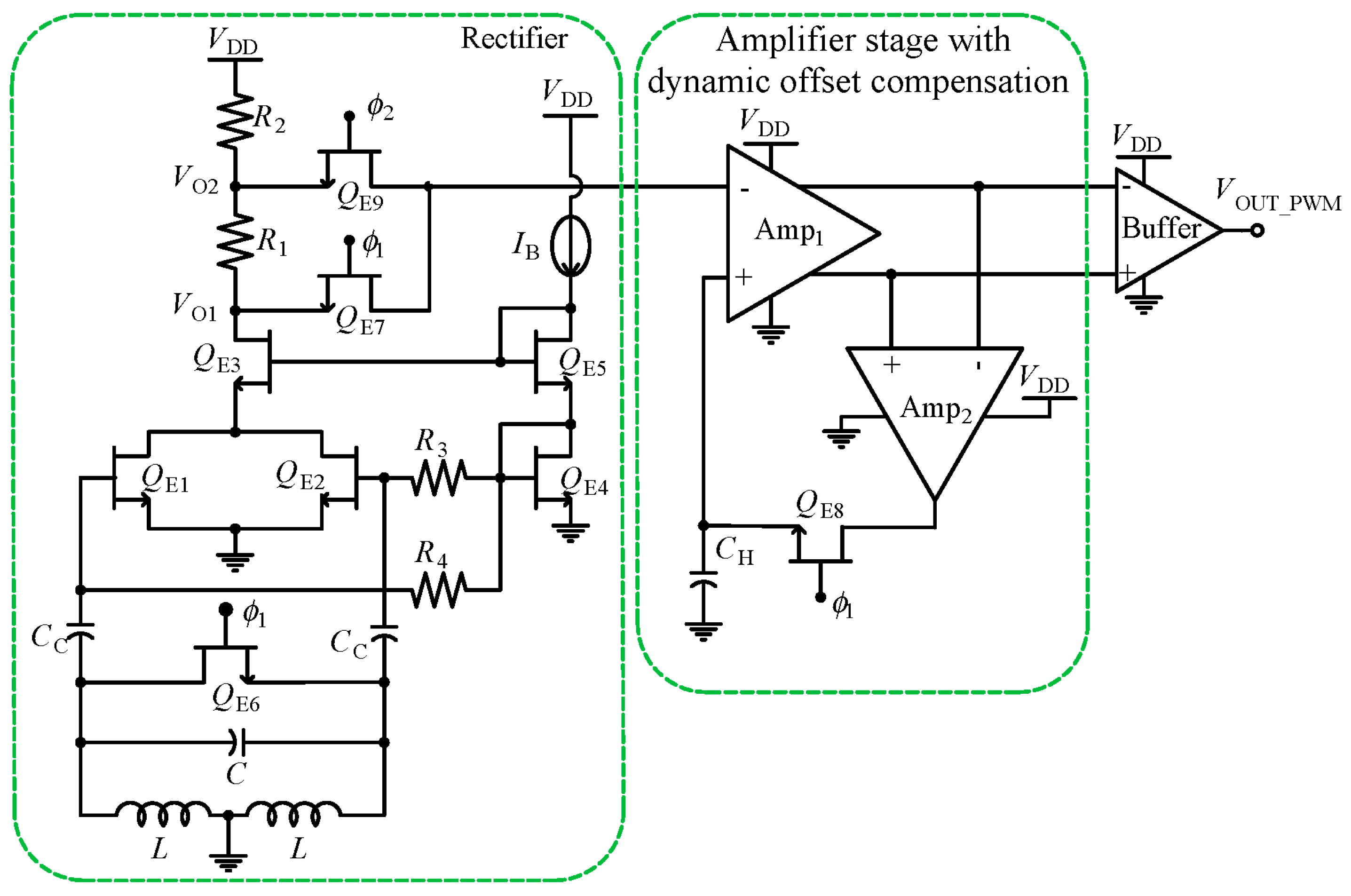
The proposed system performs three isolation channels, namely the driver control channel, the power supply control channel, and the diagnostic bidirectional channel, which are shown in Figure 2. The three-channel galvanic isolation interface is thought to be embedded with a driver/power switch in the final application to achieve a high-performance fully integrated GaN power switching system. The interface will be assembled in a system-in-package (SiP) approach, setting a DTI of around 250 µm to achieve an isolation rating of up to 12.5 kV assuming a standard molding compound with a dielectric strength of roughly 50 V/µm [43].
The two chips were fabricated using a 0.5 µm GaN on Si technology by TSMC, which includes enhancement (E) and depletion (D) n-channel transistors, MIM capacitors, and 2DEG resistors. Moreover, a 650 V power transistor is also available, enabling the galvanic isolation interface to be integrated with a power section in future applications.
The driver channel (see Figure 2a) is used to send the PWM signal through the isolation barrier to drive a power switch for a switching power converter. The RF front-end consists of two magnetically coupled planar micro-antennas, a transmitter (TX), and a receiver (RX) [46]. The TX is mainly performed by an LC oscillator that provides the 2 GHz RF carrier modulated by the PWM signal. The adopted modulation is the on–off keying (OOK). Due to the distance between the two chips, the RF signal is strongly attenuated when it reaches the RX input and hence it needs to be amplified before being recovered. The rectifier provides about 6 dB conversion gain and performs the offset compensation that is necessary to guarantee further amplification despite the bias drift due to process tolerances. Finally, a buffer is included, which preserves the channel speed performance despite external load capacitances due to the measurement setup. It can also be exploited in a future application to drive the driver/power switch.
The power supply control channel (see Figure 2b) operates with a 0.9 GHz RF carrier. It performs a voltage-mode feedback control [46] for the dc-dc flyback power converter that provides the isolated power supply for the power chip. Differently from the driver channel, RX and TX of the power supply control channel also include a start-up circuit [47] and a PWM generator [48], respectively.
The bidirectional channel (see Figure 2c) is used to transmit diagnostic data (i.e., digital-coded currents and voltages) for power section safety and reliable operation. It adopts the same architecture used in [45] for the BCD technology but with a different circuit implementation especially for the receiver, as will be discussed below. Each side of the bidirectional channel can be configured as TX or RX in a half-duplex communication scheme between the two chips. The integrated micro-antenna is exploited for the TX oscillator tank and RX input matching network. The enable signals ENTR and E N ¯ TR are properly used to switch the micro-antenna between TX and RX. Equalization capacitors, CC1,2 and CC7,8, were included to compensate for the capacitive mismatch between the LC tank and the RX input network. The RF carrier was set to about 400 MHz. In stand-by conditions, ENTR is set high and low in the chip CTR and PW, which are then configured as the transmitter and receiver, respectively. The coupling capacitors, CC3,4, are connected to the ground and the antenna in chip CTR is being resonated with the equivalent parallel capacitor Ceq = C + 0.5 CC3,4, performing the oscillator tank. At the same time, coupling capacitors, CC7,8, are grounded and the antenna in chip PW is used for the input impedance network of the RX that is on. Therefore, data transmission from chip CTR to chip PW is enabled. When a query coming from the µC is sent from chip CTR to chip PW to start diagnostic data acquisition, a time window is generated on both sides during which data communication in the opposite direction (i.e., from chip PW to CTR) is enabled by setting low ENTR in chip CTR and high ENTR in chip PW, which are then configured as the receiver and transmitter, respectively. After this time window, the diagnostic channel switches to its stand-by condition, i.e., with chip CTR configured as TX and chip PW as RX, ready for another query.

3. Receiver

A simplified block diagram of the receiver (RX) is shown in Figure 3a. It adopts an innovative approach that takes advantage of the SC technique. The receiver is mainly composed of a rectifier, an SC comparator, and a non-inverting bootstrapped buffer. A phase generator performing ϕ1 and ϕ2 is also used, which exploits a locally generated clock signal for the start-up and stand-by conditions and for the recovered PWM signal during the working condition, as described in [46]. Figure 3b shows the clock phase scheme in the working condition. Rectifier offset compensation and comparator dynamic biasing are performed during ϕ1, which is made up of a small duration pulse within the time slot in which the PWM signal is low (see Figure 3b). During ϕ1, the input terminal of the output buffer is connected to the ground thanks to switch QE9 to maintain the low level of the PWM signal at the receiver output. When ϕ1 goes low, ϕ2 switches the receiver in its operative configuration, ready to recover the next incoming PWM signal.
The rectifier exploits a common-source topology based on the input pair, QE1,2, and a resistive load, RL. A current generator, QD1-R3, is used to increase the bias current in QE1,2 while keeping high RL for better gain. The rectifier gives a first gain contribution of about 12 dB, which allows a negative output signal of around 600 mV to be achieved from an RX input signal of about 150 mV, being the TX output as high as 12 V.
Offset compensation at the rectifier output is mandatory for the next comparator operation. It is performed thanks to the feedback loop composed of the differential voltage-shifted buffer (DVSB) in Figure 3c and the rectifier itself used as a gain stage. The loop frequency compensation is easily implemented by exploiting the hold capacitor, CH1, since DVSB is characterized by the only high-impedance node at the rectifier output. Bias currents in DVSB are provided by the current generators, QD1–3-R1–3, using depletion transistors with degeneration.
The signal current in the differential pair, QE1,2, of DVSB is transferred into transistor QE3, thanks to the local feedback achieved by QE3 and QE4, and then mirrored in the rectifier input transistors, QE1,2, in Figure 3a. The final dc loop gain can then be written as
T = g m 1 , 2 · R L
and is equal to the rectifier gain.
The antenna is ac-coupled to the rectifier input thanks to the capacitors, CC, and the bias resistances, R1,2. The inductor central tap is connected to the ground for the driver and control channels, and to VDD for the bidirectional channel. This low-impedance connection increases the rejection of common-mode disturbances.
The rectifier is followed by an SC high-gain amplifier operated as a comparator. It is composed of QE3 and current source QD2-R4, with switches QE7 and QE8 that perform a dynamic biasing during ϕ1 to guarantee robustness to process tolerances and temperature variations. The bias voltage is stored in CH2, whose left terminal is connected to the reference voltage, VREF2, during ϕ1. Since QE3 is biased in the saturation region in ϕ1, the comparator provides high speed during ϕ2.
Assuming the receiver input signal is low at the beginning of the operating phase, ϕ2, a threshold voltage, ∆VT, equal to VREF1VREF2 (∆VT = 200 mV) is applied to the SC comparator input, which maintains low the receiver output as long as the PWM signal at the receiver input is low. Therefore, ∆VT performs a hysteresis threshold that guarantees an appropriate noise immunity.
The proposed receiver is greatly improved compared to the previous version shown in Figure 4 [46] in terms of robustness to process tolerances of the GaN technology.
A first problem of the previous receiver concerns the offset compensation circuit. During phase ϕ1, voltage VO1 is stored in the compensation capacitor, CH, thanks to the feedback loop performed by Amp1,2, thus allowing offset-free signal amplification for Amp1. However, the value of VO1 depends on both the mismatches in the cascode current mirror, QE1–5, and the absolute tolerances on the load resistances, R1 and R2. If VO1 approaches VDD, switch QE7 cannot be turned on during ϕ1, thus compromising the offset compensation. Moreover, negative and positive output bias voltage variations also reduce the output swing.
Another drawback correlated to the previous implementation is the accuracy of the rectifier bias current. Current mirrors in the amplifiers were avoided and substituted with more accurate current sources using degenerated depletion transistors. However, the use of a current mirror could not have been avoided in the rectifier. Therefore, the large transistor mismatch in the cascode current mirror, QE1–5, gives rise to a large variation not only in the output bias voltage mentioned before but also in the rectifier transconductance and hence in its gain.
Finally, process tolerances also cause common-mode bias voltage drifts and hence swing limitations in Amp1,2. The amplifiers exploit a differential stage with load resistances. Its differential output is accurate thanks to the differential control feedback for the offset compensation. However, the common-mode output voltage suffers from process tolerances, despite the use of more accurate current sources with depletion transistors instead of current mirrors, as mentioned before. Consequently, a drift of the output bias voltage may occur, which, besides limiting the maximum achievable gain, also leads to a swing reduction at the amplifier output.
All these limitations are overcome with the proposed improved receiver in Figure 3. The first issue on the offset compensation robustness is overcome with the feedback loop around the rectifier, which sets its bias output voltage to the reference voltage, VREF1 (VREF1 = 3 V). Indeed, this bias voltage is stored in the hold capacitor, CH1, during ϕ1 and then maintained at the output during ϕ2. Differently from the previous solution in Figure 4, this guarantees a correct switching operation for QE6 (QE7 in the previous design) regardless of process tolerances. Moreover, the bias current accuracy in the rectifier was also improved since it no longer depends on the current mirror but on the sum of the current imposed by the feedback loop in RL ((VDDVREF1)/RL) and the current of QD1-R3. This also allows RL and the rectifier bias current to be sized quite freely to increase the rectifier gain, without affecting the output bias voltage accuracy.
The output swing limitation in the amplifiers due to common-mode drifts in the previous receiver is here overcome by substituting the differential stage with the SC comparator that also provides a high gain.
Finally, it is also worth mentioning that ∆VT in this work is accurately defined by the difference of reference voltages, whereas, in the previous receiver in Figure 4, it was set by the difference between VO1 and VO2, which is affected by process tolerances on both R1 and the current mirror, QE1–5.
A schematic of the bootstrapped output buffer is shown in Figure 5. It is made up of two NOT gates with current source load, QD1,2-R1,2, a dual-feed source follower (DFSF), QE,3,4, a diode-connected transistor, QE5, and a bootstrap capacitor, CB [49]. The output buffer was included to drive the large external load capacitance, CL, due to the measurement setup, without significantly degrading the rise and fall times of the output signal. When VIN is low, QE3 is in triode, and capacitor CB is charged through transistor QE5 to VDDVT. When VIN goes high, QE2 and QE3 are turned off, QD2 goes fast in triode, and the gate-source voltage of QE4 becomes equal to the voltage across CB, which remains constant to around VDD-VT until VIN is high since the charge into CB is frozen, being terminal A floating. Therefore, QE4 drives CL with a high current until it goes into the triode region, with the output voltage, VOUT, reaching VDD.

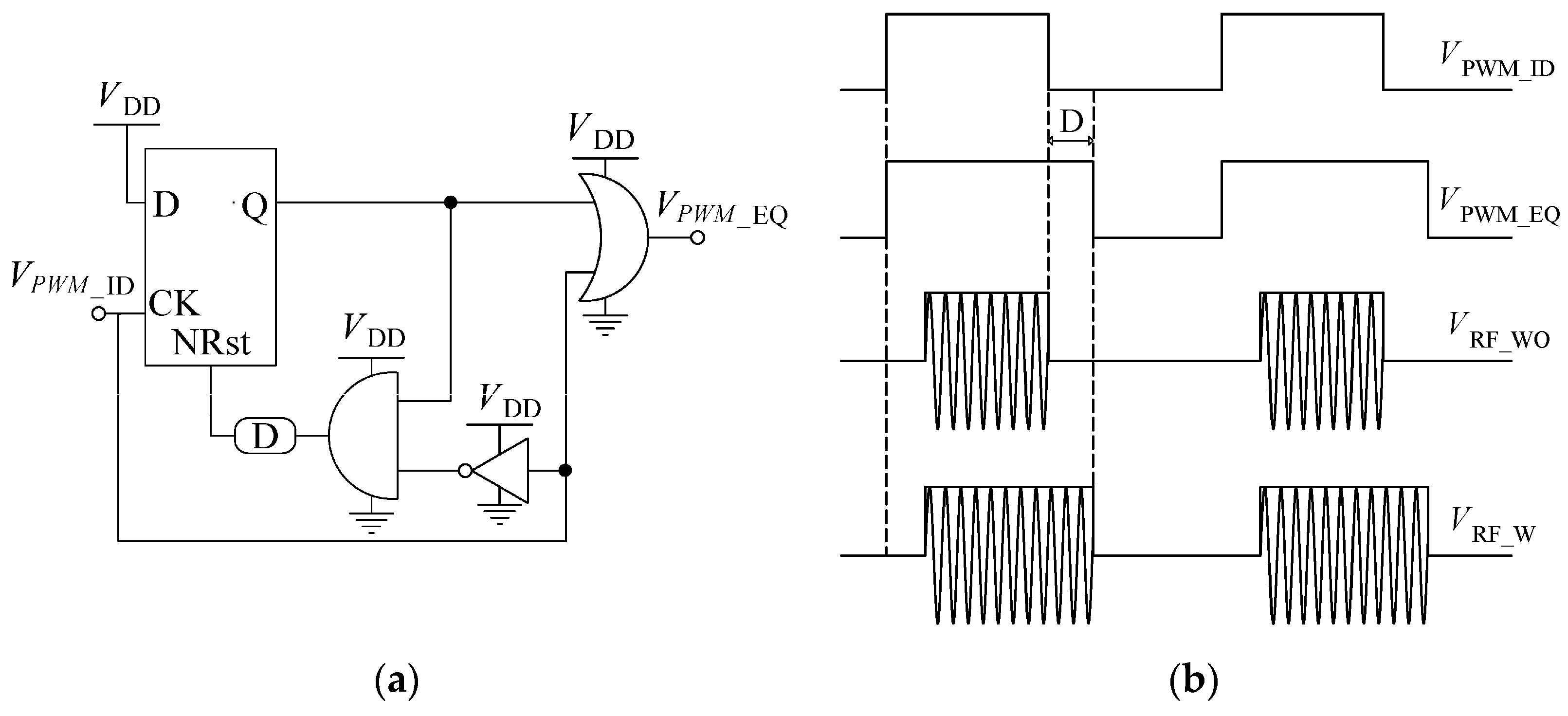
4. Duty Cycle Distortion Compensator

As far as the transmitter (TX) is concerned, it uses the D-class oscillator described in [46] but also includes an improvement of the PWM signal accuracy thanks to a circuit for the compensation of the duty cycle distortion. This distortion is mainly due to the modulation process induced by the PWM signal in the oscillator, while only a minor contribution comes from the receiver. Specifically, the PWM distortion is mainly caused by the turn-on time of the oscillator, which is much higher than the turn-off time. The duty cycle compensator is shown in Figure 6a. It is composed of a flip-flop, a delay circuit (D), and some gates. The approach is to delay the falling edge of the PWM input signal, VPWM_ID, by an amount equal to the turn-on time of the oscillator. The equalized PWM signal, VPWM_EQ, at the output of the compensator is then used to drive the oscillator. In this way, a nominally accurate correction is achieved. Figure 6b shows VPWM_ID, VPWM_EQ, in which the falling edge was delayed by D, and the modulated RF carrier at the output of the oscillator, without (VRF_WO) and with (VRF_W) duty cycle distortion compensation. Despite the delay, D is not well correlated with the turn-on time of the oscillator, and an effective correction of the duty cycle distortion is achieved. The circuit in Figure 6a is useful for the correction of negative values of the duty cycle distortion as happens in this work. In the case of positive values, a similar solution can be easily arranged.

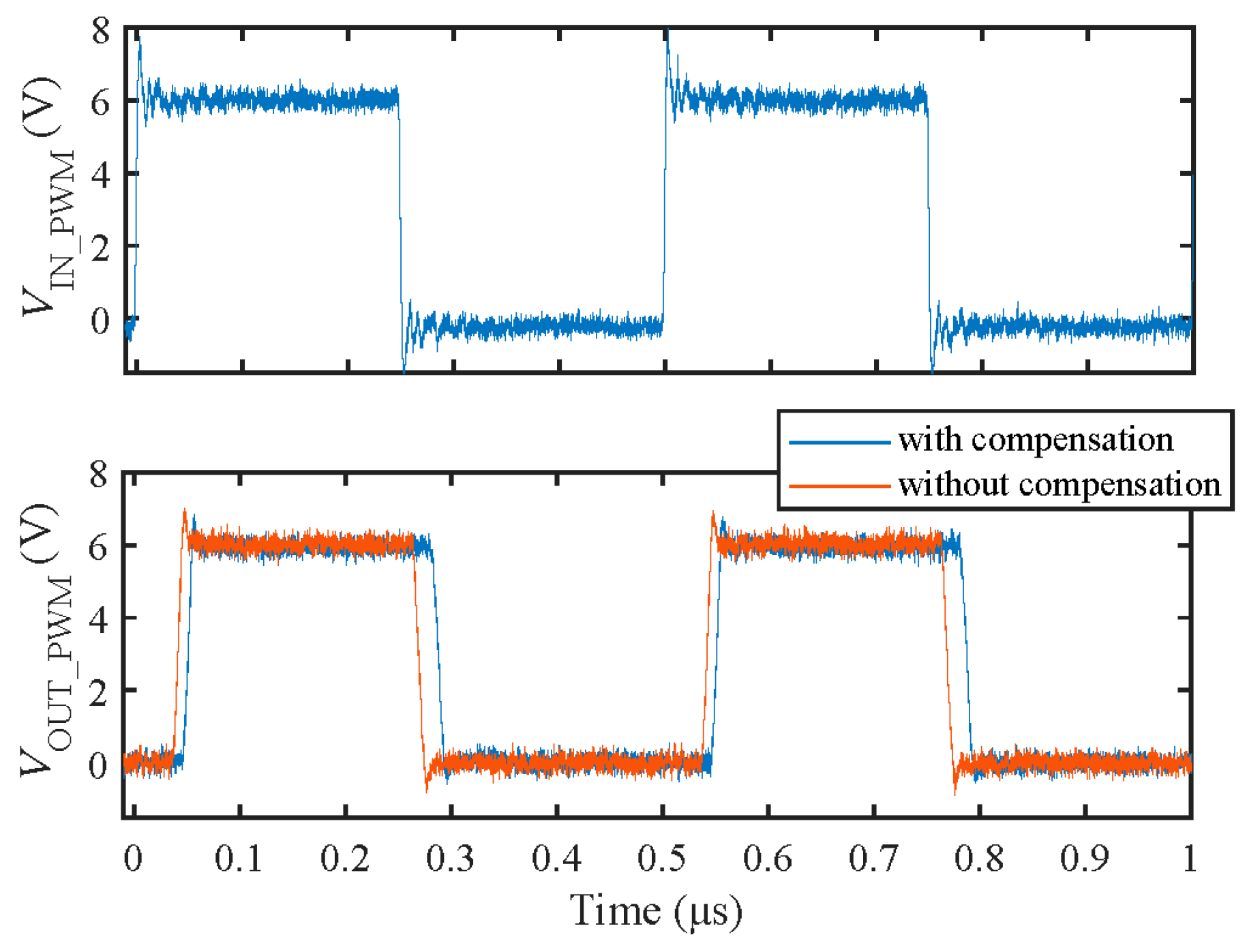
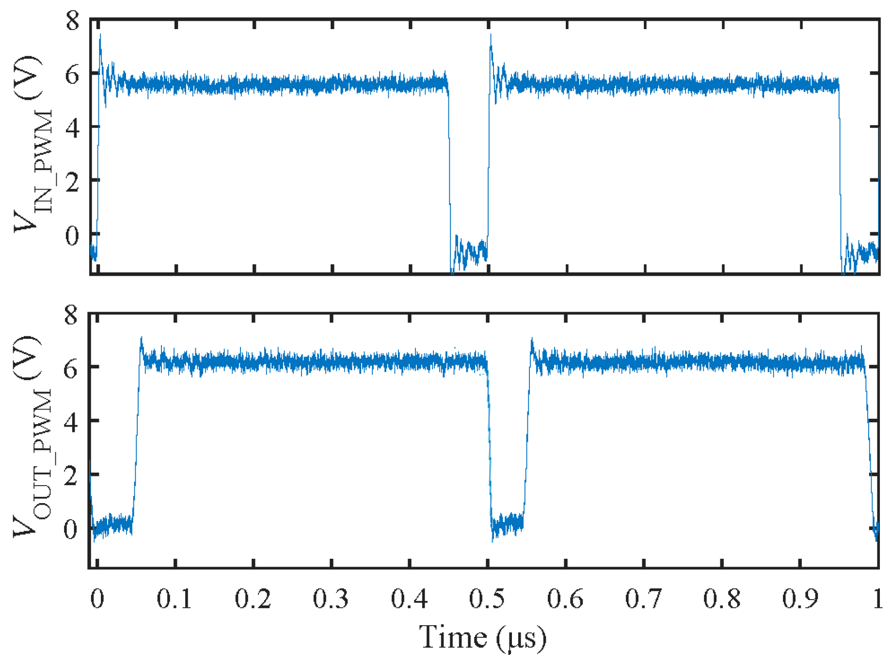
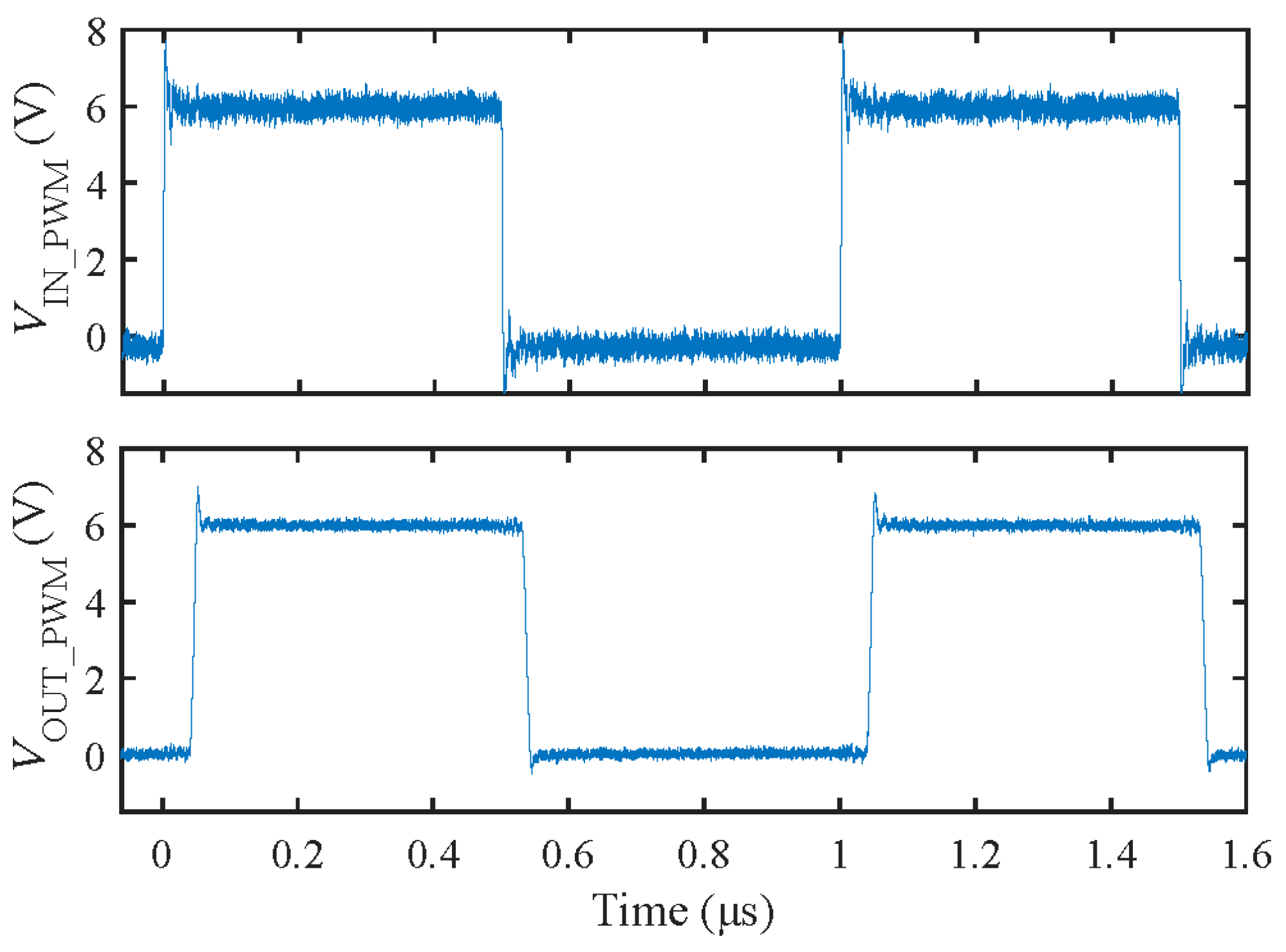
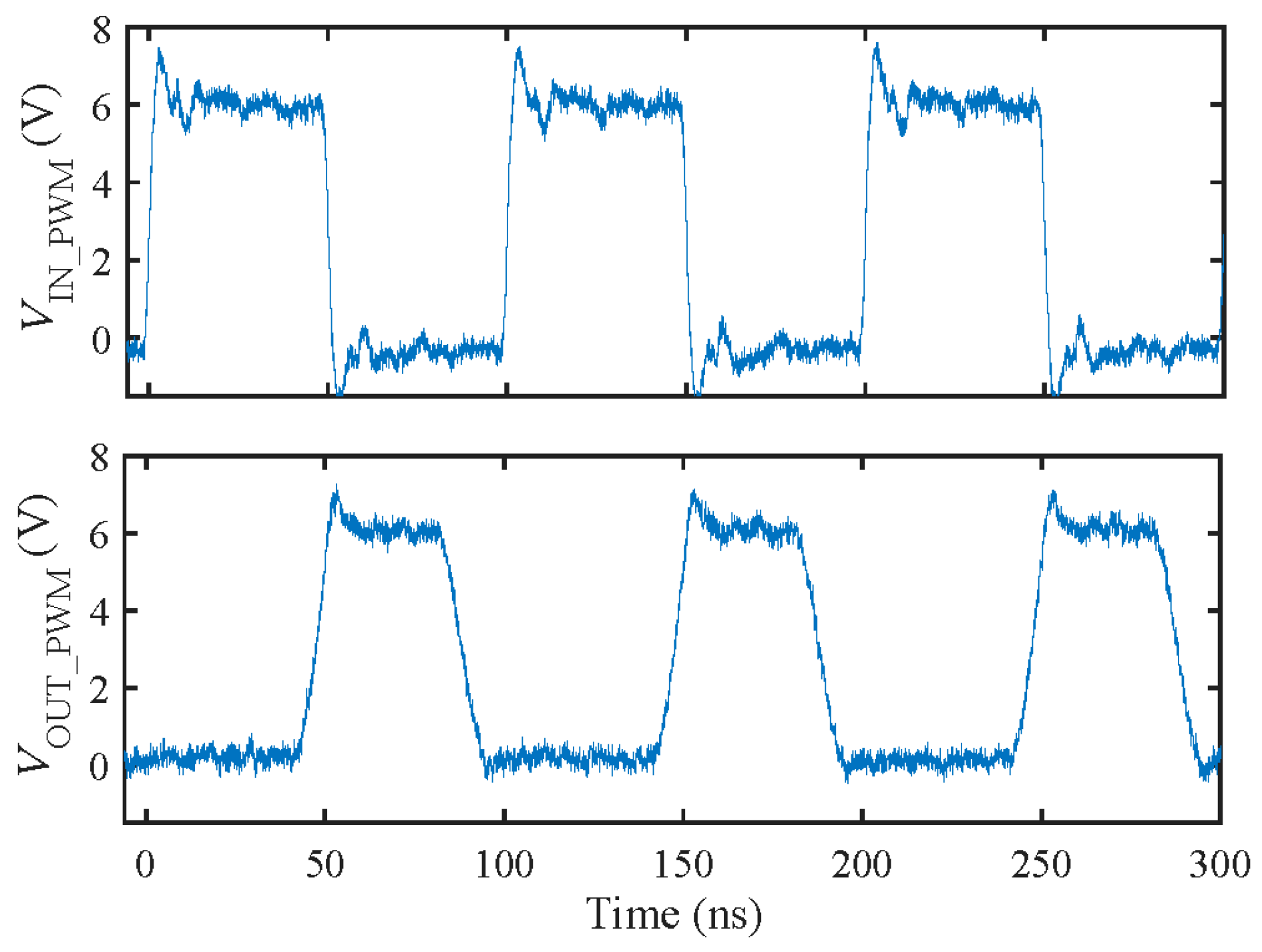
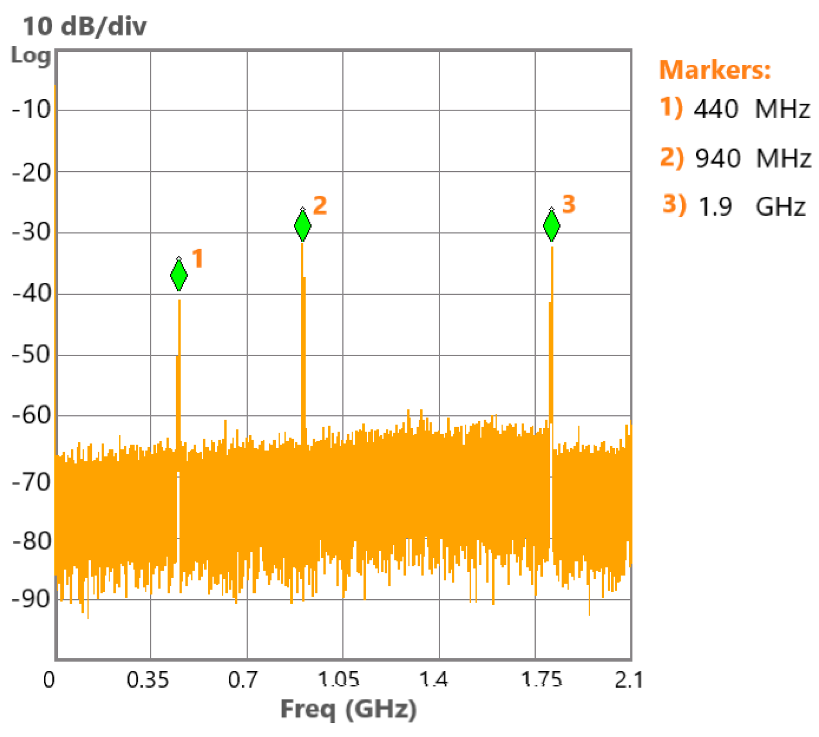
5. Experimental Results

The galvanic isolation interface was assembled chip-on-board by placing the two chips at 250 µm, as shown in the photograph in Figure 7, where the three channels are highlighted with dashed lines. The top one is the driver channel, the middle one is the power supply control channel, and the bottom one is the bidirectional diagnostic channel. Each chip occupies an area of about 3.6 mm × 2.1 mm, including protection circuits and pads.
A supply voltage of 6 V was adopted for each channel. The measured current consumptions for driver and bidirectional channels with 50% duty cycle signals are 7 mA and 8 mA, respectively, including about 1 mA of current for the bootstrapped test buffer. The current consumption for the power supply control channel is 7.5 mA, as reported in [46].
Figure 8, Figure 9 and Figure 10 show the 2 MHz PWM signal at the input and output of the driver channel with 10%, 50%, and 90%, of the duty cycle, respectively. The measured propagation delay of the output signal is about 45 ns. The bottom graph in Figure 9 highlights the comparison between the PWM output signals with and without the duty cycle distortion compensation. Thanks to the distortion compensator, the PWM signal distortion reduces by about 8 ns, from 18 ns to 10 ns. Moreover, it can also be seen that, thanks to the bootstrapped test buffer, all the measured output waveforms switch from the ground to the supply voltage with a sharp response, i.e., with a rise and fall time of about 10 ns, despite the probe input capacitance that is as high as 10 pF.
Figure 11 shows the 1 MHz PWM signal with a 50% duty cycle at the input and output of the bidirectional channel. High-frequency operation up to 10 MHz was also demonstrated as shown in Figure 12. No compensation distortion was used for this channel.
The channel carrier frequencies were measured thanks to an integrated test circuit based on a simple common-drain stage. An input capacitive partition was used, which provides a proper attenuation to avoid signal swing issues. The resulting carrier spectra are shown in Figure 13. The carrier frequencies for the driver channel, the power supply control channel, and the bidirectional channel are about 1.9 GHz, 940 MHz, and 440 MHz, respectively. The frequency separation between channels reduces crosstalk problems [46]. Finally, Table 1 summarizes the measured main electrical parameters of the galvanic isolation interface, also reporting a comparison with some typical state-of-the-art solutions.
The performance of the proposed galvanic isolation interface is aligned with the best works in the literature, although the only integrated implementation in GaN technology [46] is the previous work of the authors. With respect to the latter, this work includes the bidirectional diagnostic channel, achieves a better PWM signal distortion thanks to the distortion compensator, and provides a more robust receiver against process tolerances. The work in [45] includes a bidirectional diagnostic channel but it is implemented in BCD and hence is not suitable for the integration with the driver/power switch, which is possible instead with the GaN technology.

6. Conclusions

A three-channel galvanic isolation interface based on the chip-to-chip RF communication approach and magnetically coupled planar micro-antennas was presented. It implements the driver, the bidirectional diagnostic, and the control channel, thus performing the complete functionalities that are required in a high-performance fully integrated GaN power switching system with galvanic isolation. The interface is implemented with two chips placed at 250 µm and achieves a maximum rate of 2 MHz and 10 MHz for the driver and diagnostic channel, respectively.

Author Contributions

Validation, A.C.; Investigation, K.S., N.S. and G.P.; Writing—original draft, K.S.; Writing—review and editing, G.P.; Supervision, G.P. All authors have read and agreed to the published version of the manuscript.

Funding

This work has been carried out in the framework of the ECSEL European Project “Gallium Nitride for Advanced Power Applications” (GaN4AP), ECSEL JU No. 101007310.

Data Availability Statement

Data are contained within the article.

Acknowledgments

The authors would like to thank Mariantonietta Rizzo and Egidio De Giorgio of STMicroelectronics, Catania, Italy, for their support in layout.

Conflicts of Interest

Authors Nunzio Spina and Alessandro Castorina were employed by the company STMicroelectronics. The remaining authors declare that the research was conducted in the absence of any commercial or financial relationships that could be construed as a potential conflict of interest.

References

  1. Sun, R.; Liang, Y.C.; Yeo, Y.-C.; Zhao, C.; Chen, W.; Zhang, B. All-GaN Power Integration: Devices to Functional Subcircuits and Converter ICs. IEEE J. Emerg. Sel. Top. Power Electron. 2020, 8, 31–41. [Google Scholar] [CrossRef]
  2. Ikeda, N.; Niiyama, Y.; Kambayashi, H.; Sato, Y.; Nomura, T.; Kato, S.; Yoshida, S. GaN Power Transistors on Si Substrates for Switching Applications. Proc. IEEE 2010, 98, 1151–1161. [Google Scholar] [CrossRef]
  3. Hassan, A.; Savaria, Y.; Sawan, M. GaN Integration Technology, an Ideal Candidate for High-Temperature Applications: A Review. IEEE Access 2018, 6, 78790–78802. [Google Scholar]
  4. Meneghini, M.; Meneghesso, G.; Zanoni, E. (Eds.) Gallium Nitride Enabled High Frequency and High Efficiency Power Conversion, 1st ed.; Springer: Berlin/Heidelberg, Germany, 2018. [Google Scholar]
  5. Chen, K.J.; Haberlen, O.; Lidow, A.; Tsai, C.L.; Ueda, T.; Uemoto, Y.; Wu, Y. GaN-on-Si Power Technology: Devices and Applications. IEEE Trans. Electron Devices 2017, 64, 779–795. [Google Scholar]
  6. Sun, R.; Lai, J.; Chen, W.; Zhang, B. GaN Power Integration for High Frequency and High Efficiency Power Applications: A Review. IEEE Access 2020, 8, 15529–15542. [Google Scholar]
  7. Ke, X.; Sankman, J.; Chen, Y.; He, L.; Ma, D.B. A Tri-Slope Gate Driving GaN DC–DC Converter with Spurious Noise Compression and Ringing Suppression for Automotive Applications. IEEE J. Solid-State Circuits 2018, 53, 247–260. [Google Scholar]
  8. Seidel, A.; Wicht, B. Integrated Gate Drivers Based on High-Voltage Energy Storing for GaN Transistors. IEEE J. Solid-State Circuits 2018, 53, 3446–3454. [Google Scholar]
  9. Chen, C.-J.; Chiu, P.-K.; Chen, Y.-M.; Wang, P.-Y.; Chang, Y.-C. An Integrated Driver with Adaptive Dead-Time Control for GaN-Based Synchronous Buck Converter. IEEE Trans. Circuits Syst. II Express Briefs 2022, 69, 539–543. [Google Scholar] [CrossRef]
  10. Majima, H.; Ishihara, H.; Ikeuchi, K.; Ogawa, T.; Sawahara, Y.; Ogawa, T.; Takaya, S.; Onizuka, K.; Watanabe, O. Cascoded GaN half-bridge with 17 MHz wide-band galvanically isolated current sensor. Jpn. J. Appl. Phys. 2022, 61, SC1052. [Google Scholar]
  11. Meneghini, M.; Ronchi, N.; Stocco, A.; Meneghesso, G.; Mishra, U.K.; Pei, Y.; Zanoni, E. Investigation of Trapping and Hot-Electron Effects in GaN HEMTs by Means of a Combined Electrooptical Method. IEEE Trans. Electron Devices 2011, 58, 2996–3003. [Google Scholar]
  12. Sayadi, L.; Iannaccone, G.; Sicre, S.; Häberlen, O.; Curatola, G. Threshold Voltage Instability in p-GaN Gate AlGaN/GaN HFETs. IEEE Trans. Electron Devices 2018, 65, 2454–2460. [Google Scholar] [CrossRef]
  13. Tang, S.W.; Bakeroot, B.; Huang, Z.H.; Chen, S.C.; Lin, W.S.; Lo, T.C.; Borga, M.; Wellekens, D.; Posthuma, N.; Decoutere, S.; et al. Using Gate Leakage Conduction to Understand Positive Gate Bias Induced Threshold Voltage Shift in p-GaN Gate HEMTs. IEEE Trans. Electron Devices 2023, 70, 449–453. [Google Scholar] [CrossRef]
  14. Trani, R.; Catalano, A.P.; Castellazzi, A.; D’Alessandro, V. Thermal management solutions for a lightweight 3 L GaN inverter. In Proceedings of the IEEE 10th International Conference on Power Electronics and ECCE, Asia (ICPE 2019–ECCE Asia), Busan, Republic of Korea, 27–31 May 2019; pp. 2173–2178. [Google Scholar]
  15. Kozak, J.P.; Zhang, R.; Porter, M.; Song, Q.; Liu, J.; Wang, B.; Wang, R.; Saito, W.; Zhang, Y. Stability, Reliability, and Robustness of GaN Power Devices: A Review. IEEE Trans. Power Electron. 2023, 38, 8442–8471. [Google Scholar] [CrossRef]
  16. Wong, K.-Y.; Chen, W.; Chen, K.J. Integrated Voltage Reference Generator for GaN Smart Power Chip Technology. IEEE Trans. Electron Devices 2010, 57, 952–955. [Google Scholar] [CrossRef]
  17. Liu, X.; Chen, K.J. GaN Single-Polarity Power Supply Bootstrapped Comparator for High-Temperature Electronics. IEEE Electron Device Lett. 2011, 32, 27–29. [Google Scholar] [CrossRef]
  18. Hong, Y.-P.; Mukai, K.; Gheidi, H.; Shinjo, S.; Asbeck, P.M. High efficiency GaN switching converter IC with bootstrap driver for envelope tracking applications. In Proceedings of the 2013 IEEE Radio Frequency Integrated Circuits Symposium (RFIC), Seattle, WA, USA, 2–4 June 2013. [Google Scholar]
  19. Wang, H.; Kwan, A.M.H.; Jiang, Q.; Chen, K.J. A GaN Pulse Width Modulation Integrated Circuit for GaN Power Converters. IEEE Trans. Electron Devices 2015, 62, 1143–1149. [Google Scholar]
  20. Zhang, Y.; Rodríguez, M.; Maksimović, D. Very High Frequency PWM Buck Converters Using Monolithic GaN Half-Bridge Power Stages with Integrated Gate Drivers. IEEE Trans. Power Electron. 2016, 31, 7926–7942. [Google Scholar]
  21. Tang, G.; Kwan, A.M.H.; Wong, R.K.Y.; Lei, J.; Su, R.Y.; Yao, F.W.; Lin, Y.M.; Yu, J.L.; Tsai, T.; Tuan, H.C.; et al. Digital Integrated Circuits on an E-Mode GaN Power HEMT Platform. IEEE Electron Device Lett. 2017, 38, 1282–1285. [Google Scholar] [CrossRef]
  22. Zhu, M.; Matioli, E. Monolithic integration of GaN-based NMOS digital logic gate circuits with E-mode power GaN MOSHEMTs. In Proceedings of the IEEE 30th International Symposium on Power Semiconductor Devices and ICs (ISPSD), Chicago, IL, USA, 13–17 May 2018; pp. 236–239. [Google Scholar]
  23. Li, X.; Geens, K.; Guo, W.; You, S.; Zhao, M.; Fahle, D.; Odnoblyudov, V.; Groeseneken, G.; Decoutere, S. Demonstration of GaN Integrated Half-Bridge with On-Chip Drivers on 200-mm Engineered Substrates. IEEE Electron Device Lett. 2019, 40, 1499–1502. [Google Scholar] [CrossRef]
  24. Pennisi, S.; Pulvirenti, F.; Samperi, K. Frequency compensation scheme for a full GaN OpAmp driving 1-nF load. In Proceedings of the IEEE International Symposium on Circuits and Systems (ISCAS), Austin, TX, USA, 27 May–1 June 2022; pp. 2042–2046. [Google Scholar]
  25. Catalano, A.P.; Scognamillo, C.; d’Alessandro, V.; Codecasa, L. In-Situ Extraction of the Thermal Impedance of GaN Power HEMTs Embedded in PCB-based Power Circuits. In Proceedings of the IEEE 35th International Symposium on Power Semiconductor Devices and ICs (ISPSD), Hong Kong, China, 28 May–1 June 2023; pp. 310–313. [Google Scholar]
  26. Yan, D.; Ma, D.B. A Monolithic GaN Power IC with On-Chip Gate Driving, Level Shifting, and Temperature Sensing, Achieving Direct 48-V/1-V DC–DC Conversion. IEEE J. Solid-State Circuits 2022, 57, 3865–3876. [Google Scholar] [CrossRef]
  27. Li, A.; Shen, Y.; Li, Z.; Li, F.; Sun, R.; Mitrovic, I.Z.; Wen, H.; Lam, S.; Liu, W. A 4-Transistor Monolithic Solution to Highly Linear On-Chip Temperature Sensing in GaN Power Integrated Circuits. IEEE Electron Device Lett. 2023, 44, 333–336. [Google Scholar]
  28. Pan, C.; Yu, X.; Li, F.; Gong, H.; Wang, D.; Zhou, J.; Li, Z.; Liu, W.; Chen, D.; Gu, S.; et al. Monolithically Integrated Logic Circuits Based on p-NiO Gated E-Mode GaN HEMTs. IEEE Electron Device Lett. 2024, 45, 164–167. [Google Scholar]
  29. Analog Devices. Surging Across the Barrier: Digital Isolators Set the Standard for Reinforced Insulation. Available online: https://www.analog.com (accessed on 8 January 2025).
  30. NVE Corporation, Isolator High Voltage Safety Standards. Available online: https://www.nve.com (accessed on 6 February 2025).
  31. Chen, B. Fully integrated isolated dc-dc converter using micro-transformers. In Proceedings of the IEEE Applied Power Electronics Conference and Exposition, (APEC), Austin, TX, USA, 24–28 February 2008; pp. 335–338. [Google Scholar]
  32. Lombardo, P.; Fiore, V.; Ragonese, E.; Palmisano, G. A fully integrated half-duplex data/power transfer system with up to 40 Mbps data rate, 23 mW output power and on-chip 5 kV galvanic isolation. In Proceedings of the IEEE International Solid-State Circuits Conference: Digest of Technical Papers, San Francisco, CA, USA, 31 January–4 February 2016; pp. 300–301. [Google Scholar]
  33. Shi, G.; Yan, R.; Xi, J.; He, L.; Ding, W.; Pan, W.; Liu, Z.; Yang, F.; Chen, D. A compact 6 ns propagation delay 200 Mbps 100 kV/μs CMR capacitively coupled direction configurable 4-channel digital isolator in standard CMOS. In Proceedings of the IEEE International Conference on Electronics, Circuits and Systems, Bordeaux, France, 9–12 December 2018; pp. 721–724. [Google Scholar]
  34. Fiore, V.; Ragonese, E.; Palmisano, G. A fully integrated watt-level power transfer system with on-chip galvanic isolation in silicon technology. IEEE Trans. Power Electron. 2017, 32, 1984–1995. [Google Scholar]
  35. Zhuo, Y.; Ma, S.; Zhao, T.; Qin, W.; Zhao, Y.; Guo, Y.; Yan, H.; Chen, B. A 52% Peak Efficiency > 1-W Isolated Power Transfer System Using Fully Integrated Transformer with Magnetic Core. IEEE J. Solid-State Circuits 2019, 54, 3326–3335. [Google Scholar]
  36. Greco, N.; Parisi, A.; Lombardo, P.; Spina, N.; Ragonese, E.; Palmisano, G. A double-isolated DC-DC converter based on integrated LC resonant barriers. IEEE Trans. Circuits Syst. I Regul. Pap. 2018, 65, 4423–4433. [Google Scholar]
  37. Ragonese, E.; Spina, N.; Castorina, A.; Lombardo, P.; Greco, N.; Parisi, A.; Palmisano, G. A fully integrated galvanically isolated DC-DC converter with data communication. IEEE Trans. Circuits Syst. I Regul. Pap. 2018, 65, 1432–1441. [Google Scholar]
  38. Parisi, A.; Ragonese, E.; Spina, N.; Palmisano, G. Galvanically isolated DC-DC converter using a single isolation transformer for multi-channel communication. IEEE Trans. Circuits Syst. I Regul. Pap. 2020, 67, 4434–4444. [Google Scholar]
  39. Uchida, S.; Kaeriyama, S.; Nagase, H.; Takeda, K.; Nakashiba, Y.; Maeda, T.; Ishihara, K. A face-to-face chip stacking 7 kV RMS digital isolator for automotive and industrial motor drive applications. In Proceedings of the IEEE 26th International Symposium on Power Semiconductor Devices IC’s (ISPSD), Waikoloa, HI, USA, 15–19 June 2014; pp. 442–445. [Google Scholar]
  40. Renna, C.M.-A.; Scuderi, A.; Magro, C.; Spina, N.; Ragonese, E.; Marano, B.; Palmisano, G. Microstructure Device Comprising a Face to Face Electromagnetic Near Field Coupling Between Stacked Device Portions and Method of Forming the Device. U.S. Patent 9018730 B2, April 2015. [Google Scholar]
  41. Spina, N.; Girlando, G.; Smerzi, S.A.; Palmisano, G. Integrated Galvanic Isolator Using Wireless Transmission. U.S. Patent 8364195 B2, 28 January 2013. [Google Scholar]
  42. Mukherjee, S.; Bhat, A.N.; Shrivastava, K.A.; Bonu, M.; Sutton, B.; Gopinathan, V.; Thiagarajan, G.; Patki, A.; Malakar, J.; Krishnapura, N. A 500 Mb/s 200 pJ/b Die-to-Die Bidirectional Link with 24 kV Surge Isolation and 50 kV/μs CMR using Resonant Inductive Coupling in 0.18 μm CMOS. In Proceedings of the IEEE International Solid-State Circuits Conference: Digest of Technical Papers, San Francisco, CA, USA, 5–9 February 2017; pp. 434–435. [Google Scholar]
  43. Ragonese, E.; Spina, N.; Parisi, A.; Palmisano, G. A CMOS data transfer system based on planar RF coupling for reinforced galvanic isolation with 25-kV surge voltage and 250-kV/µs CMTI. Electronics 2020, 9, 943. [Google Scholar] [CrossRef]
  44. Ragonese, E.; Parisi, A.; Spina, N.; Palmisano, G. Compact galvanically isolated architectures for low-power dc-dc converters with data transmission. Electronics 2021, 10, 2328. [Google Scholar] [CrossRef]
  45. Spina, N.; Raimondi, M.; Castorina, A.; Ragonese, E.; Palmisano, G. A 3-Channel Package-Scale Galvanic Isolation Interface for Wide Bandgap Gate Drivers. IEEE Trans. Very Large Scale Integr. VLSI Syst. 2024, 32, 1389–1399. [Google Scholar] [CrossRef]
  46. Spina, N.; Samperi, K.; Pavlin, A.; Pennisi, S.; Palmisano, G. Fully Integrated Galvanic Isolation Interface in GaN Technology. IEEE Trans. Circuits Syst. I Regul. Pap. 2023, 70, 4605–4614. [Google Scholar] [CrossRef]
  47. Samperi, K.; Spina, N.; Pennisi, S.; Palmisano, G. Integrated GaN digital soft start-up for switching power converters. In Proceedings of the 18th Conference on Ph.D Research in Microelectronics and Electronics (PRIME), Valencia, Spain, 18–21 June 2023; pp. 193–196. [Google Scholar]
  48. Samperi, K.; Spina, N.; Castorina, A.; Pavlin, A.; Pennisi, S.; Palmisano, G. GaN Monolithic PWM Generator with Dynamic Offset Compensation. IEEE Access 2023, 11, 126892–126899. [Google Scholar] [CrossRef]
  49. Samperi, K.; Pennisi, S.; Pulvirenti, F. High-Speed all-GaN Gate Driver with reduced power consumption. In Proceedings of the 21st IEEE Interregional NEWCAS Conference (NEWCAS), Edinburgh, UK, 26–28 June 2023; pp. 1–5. [Google Scholar]
  50. ADuM4221, Isolated, Half Bridge Gate Drivers with Adjustable Dead Time, 4 A Output, Analog Devices, Norwood, MA, USA [Online]. Available online: https://www.analog.com/en/index.html (accessed on 8 January 2025).
  51. UCC2154x Reinforced Isolation Dual-Channel Gate Driver with 3.3-mm Channel-to-Channel Spacing Option, Texas Instruments, Dallas, TX, USA. Available online: https://www.ti.com/lit/ds/symlink/ucc21542.pdf?ts=1663549023521 (accessed on 8 January 2025).
Figure 1. Simplified on-package representation of the isolation interface based on chip-to-chip communication.
Electronics 14 01403 g001
Figure 2. Example of system application. (a) Driver control channel, (b) power supply control channel, and (c) bidirectional diagnostic channel.
Electronics 14 01403 g002aElectronics 14 01403 g002b
Figure 3. (a) Simplified schematic of the proposed receiver, (b) PWM signal and clock phases operation, (c) schematic of the DVSB.
Electronics 14 01403 g003
Figure 4. Simplified schematic of the previous receiver in [46].
Electronics 14 01403 g004
Figure 5. Bootstrapped digital buffer.
Electronics 14 01403 g005
Figure 6. (a) Simplified schematic of the PWM duty cycle distortion compensator. (b) PWM and RF signals.
Electronics 14 01403 g006
Figure 7. Photograph of the chip-on-board assembly of the galvanic isolation interface.
Electronics 14 01403 g007
Figure 8. A 2 MHz and 10% PWM signal in the driver channel.
Electronics 14 01403 g008
Figure 9. A 2 MHz and 50% PWM signal in the driver channel.
Electronics 14 01403 g009
Figure 10. A 2 MHz and 90% PWM signal in the driver channel.
Electronics 14 01403 g010
Figure 11. A 1 MHz data signal in the bidirectional channel.
Electronics 14 01403 g011
Figure 12. A 10 MHz data signal in the bidirectional channel.
Electronics 14 01403 g012
Figure 13. Measured channel carrier frequencies. Markers 1, 2, and 3 refer to the bidirectional channel, supply control channel, and driver channel, respectively.
Electronics 14 01403 g013
Table 1. Summarized performance and comparison with the state of the art.
Parameters[42][45][46][50][51]This Work
Applicationn.a.Gate driversGate driversGate driversGate driversGate drivers
No of isolation channels232223
Max rate500 Mbit/s0.4 MHz (1)
15 MHz (2)
2 MHz (1)1 MHz1 MHz2 MHz (1)
10 MHz (2)
Propagation delay [ns]n.a.3430442840
PWM distortion [ns]n.a.n.a18n.a.6.510
Isolation technologyChip-to-chip RF communicationChip-to-chip RF communicationChip-to-chip RF communicationPolyimide
transformers
On-chip SiO2 capacitorsChip-to-chip RF communication
Isolation levelReinforced
(>10 kVPK)
Reinforced
(>10 kVPK) (3)
Reinforced
(>10 kVPK) (3)
Basic
(5.7 VRMS)
Reinforced
(8 kVPK)
Reinforced
(>10 kVPK) (3)
CMTI
[kV/μs]
50n.a. (4)n.a. (4)150100n.a. (4)
Supply voltage [V]1.83653/5.56
Technology0.18 µm CMOS0.32 μm BCD0.5 μm GaN on Sin.a.n.a.0.5 μm GaN on Si
No. of dice222232
Area [mm2]n.a.11.65.8n.a.n.a.8.7
(1) Driver channel. (2) Bidirectional diagnostic channel. (3) Estimated assuming 50 V/µm dielectric strength molding compound and 250-μm DTI. (4) Measurement is not available.
Disclaimer/Publisher’s Note: The statements, opinions and data contained in all publications are solely those of the individual author(s) and contributor(s) and not of MDPI and/or the editor(s). MDPI and/or the editor(s) disclaim responsibility for any injury to people or property resulting from any ideas, methods, instructions or products referred to in the content.

