Article

Methodology for Designing Broadband DC Link Filters for Voltage Source Converters

Technology-Transfer Centre for E-Mobility, Technical University of Applied Sciences Würzburg-Schweinfurt (THWS), Poststraße 31, 97616 Bad Neustadt an der Saale, Germany
*
Author to whom correspondence should be addressed.
These authors contributed equally to this work.
Electronics 2025, 14(14), 2743; https://doi.org/10.3390/electronics14142743
Submission received: 2 June 2025 / Revised: 2 July 2025 / Accepted: 3 July 2025 / Published: 8 July 2025
(This article belongs to the Special Issue Gallium Nitride (GaN)-Based Power Electronic Devices and Systems)

Abstract

This paper presents a new methodology for the design process of DC ripple filters for voltage source converters. It focuses on fast-switching, wide-bandgap-material-based converters. Therefore, a wide frequency range of up to 100 MHz is taken into consideration during the whole process. Different tools like analytic calculations, time-domain modelling, and the finite element method are used for different tasks in order to generate a realistic model in terms of filter effect and reliability. The models are validated by small-signal measurements using a vector network analyser as well as realistic high-power tests. The contribution of this paper is to provide a tool for DC link filter design to estimate the filter efficiency and the current stress on the filter elements with a special focus on WBG hardware.

1. Introduction

For the design of a DC link differential mode (DM) disturbance filter, often called a DC ripple filter, of a voltage source converter (VSC), the main criteria are the current load on the filter and the remaining voltage ripple at the filter’s quiet port. Classically, the design process is based on analytic calculations to determine a filter that fulfils these criteria while also depending on the modulation scheme that is used [1,2,3,4,5,6,7,8,9,10,11,12,13,14,15,16,17].
Not considered in the named calculations is the limitation of switching overvoltage for protection of the switching devices. Low-inductance capacitors are necessary for this task. In the past, the matching filter was mostly determined empirically [18]. Especially in wide-bandgap (WBG) devices, recent papers also analyse the voltage oscillation caused by the switching of the power device via mathematical models [19,20,21,22].
WBG devices allow for higher power densities and reduced filter component sizes. This enables and, with regard to the fast switching of these devices, at the same time requires compact system design [23,24,25,26,27]. According to [28], capacitors are the most common cause of errors in VSCs, along with various other components such as printed circuit boards, semiconductors, solder joints, and connectors. There are many different types of capacitors. For use as a DC-side filter capacitor, three different types are used [29]:
  • Aluminum electrolytic capacitors:
    Electrolyte capacitors are mostly used in industrial applications. Their dielectric strength is limited to approx. 450V (although there are also special versions with a maximum applicable voltage of 600 V), which is why typical applications in the range 600–900 V usually use two capacitors connected in series. To increase the total capacity and/or current-carrying capability, several capacitors are usually connected in parallel. Compared to other types of capacitors, they achieve the highest energy density and the lowest cost per joule. However, the large space requirement due to the low current-carrying capability, wear and tear caused by the evaporation of the electrolyte solution, is disadvantageous. Furthermore, compared to the film capacitor, it has a much higher, strongly frequency-dependent ESR and thus a significantly lower efficiency and a lower current-carrying capability. Electrolyte capacitors are polarised and can only be used for DC voltage applications. The main areas of application are industrial applications.
  • Multilayer ceramic capacitors:
    Multilayer ceramic capacitors (MLCCs) have smaller construction volumes in comparison to electrolyte capacitors, larger frequency ranges, and higher operating temperatures of up to 200 °C. Disadvantages, however, are higher costs and mechanical sensitivity. Parasitic effects like DC and AC bias dependence have to be taken into account [30,31,32,33,34,35,36]. They are often manufactured in surface mounted device (SMD) designs and are used for complex applications on printed circuit boards.
  • Metallised film capacitors:
    Metallised Polypropylene film capacitors (MPPFCs) offer a balanced design for higher-voltage applications (e.g., over 500 V) in terms of cost and ESR, capacitance, ripple, current, and reliability. However, they have the disadvantages of a large volume and a moderate upper operating temperature. Parasitic effects like eddy currents and skin and proximity effects influence their filtering effect, especially for higher frequencies, and have to be taken into account [37,38,39,40,41,42,43]. Related to the current-carrying capability, the costs of MPPFCs are about one third of the costs for electrolyte capacitors. Because of this, they are preferred for applications with high distortion currents, such as in the drive train of electric vehicles [44].
For Si-based VSCs, where electrolyte capacitors are applied for DC ripple filtering, the switching overvoltage filter can be designed separately. Electrolyte capacitors feature comparably high ohmic damping [29], which reduces the risk of resonances with high resonant circuit quality. This statement cannot be applied to modern VSCs based on fast-switching wide-bandgap (WBG) devices. Especially when high switching frequencies are introduced, the tasks of switching overvoltage protection and DC ripple filtering overlap. Therefore, a holistic design approach has to be taken for filtering DC link DM disturbances.
This paper reflects the task of redesigning the DC link DM disturbance filter for a WBG-based VSC in order to improve its HF-filter efficiency. In the scope of this work, it is used as an example for explaining the model-based holistic design methodology, which is the key finding of this paper. The considered two-level VSC provides three phase legs that are connected to a common DC link, as can be seen in Figure 1. Table 1 states the most important parameters for the design of the DC link DM disturbance filter.

2. Basic Filter Design

As mentioned before, the designated filter performance should be very broadband to fulfil different tasks:
  • Low -frequency (LF) filter: Reduce the DC voltage ripple generated from the modulation scheme.
  • High-frequency (HF) filter: Limit the switching overvoltage to a fixed level.
  • Course of action:
The methodology presented is structured as a basic course of action, which is described in the following:
1.
First estimations based on analytic calculations.
2.
Component selection for LF filter.
3.
Time-based simulation model of VSC and filter.
4.
Component selection for HF filter.
5.
Determine impedance of mechanical components.
6.
Integration in time-based simulation model.
7.
Validation on experimental setup.

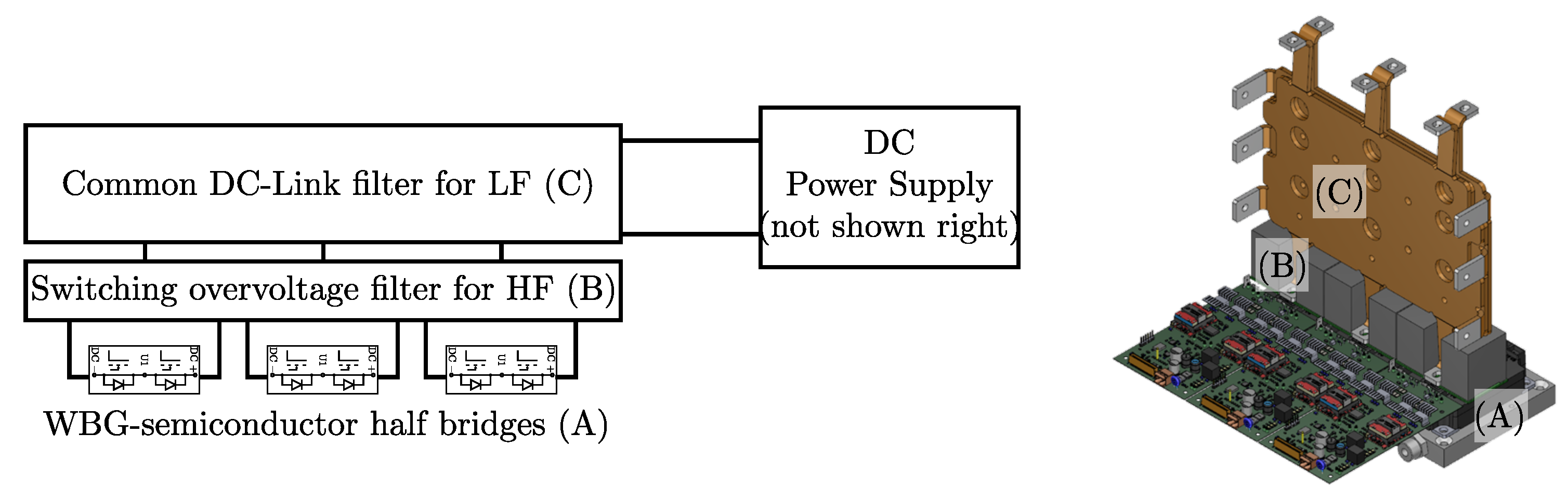
3. Exemplary Filter Design

3.1. First Estimations Based on Analytic Calculations

By using the analytic calculation described in [1], the necessary current-carrying capability of the capacitors for the LF filter can be determined. By using the analytic calculations from [2], the necessary capacity for the LF filter for a defined remaining voltage ripple U C 1 can be determined. Here, U C 1 = 8 V is defined.
  • This results in
  • Current-carrying capability: I C 1 = 325 A ;
  • Necessary capacity: C 1 = 450 μ F .

3.2. Component Selection for LF Filter

Depending on the application, electrolytic capacitors, film capacitors, or a combination of both may be preferable. Capacitors should have sufficient low impedance at the dominant amplitude of the VSC’s DC-side current amplitude spectrum. Depending on the modulation scheme and the topology, the current amplitude spectrum contains different dominant harmonic amplitudes [3,45,46,47,48]. They can be calculated analytically as described in [49] or be determined by simulation.
Here, simulation is used. Figure 2 shows the VSC’s DC-side current amplitude spectrum for switching frequencies f s = 10 kHz (a) and f s = 200 kHz (b), respectively. For the SVM modulation scheme, the dominant amplitude appears for 2 · f S . Different capacitors are compared regarding their impedance. The necessary data can be taken from manufacturers’ datasheets or be determined via impedance measurement.
Figure 3 shows the measured impedances of different capacitors, all with identical capacity. It becomes apparent that the impedance and so their filter efficiency strongly depend on parasitic attributes, namely, the parasitic inductance L C 1 . Results (A) and (B) are for capacitors with a cylindrical design. For result (C), the filter is built from several smaller capacitors with comparable low L C 1 . Here, 22 capacitors with a capacity of 22 μ F each are used. It can be seen that this filter has significantly lower impedance for f > 40 kHz and therefore improved filter efficiency. Because of these advantages, variant (C) is chosen to be used as the LF filter.

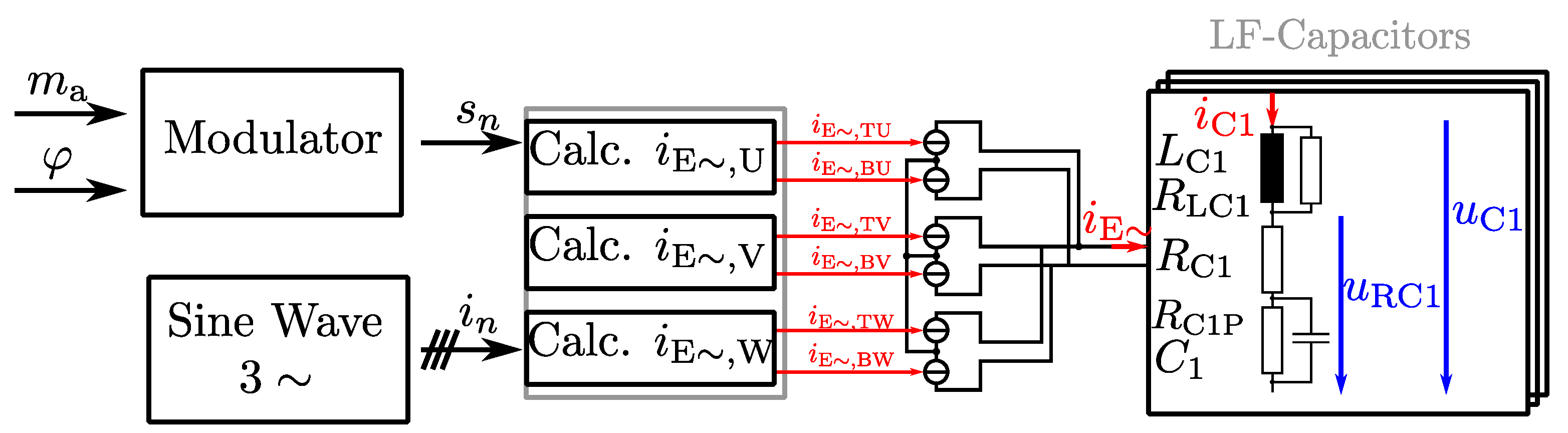
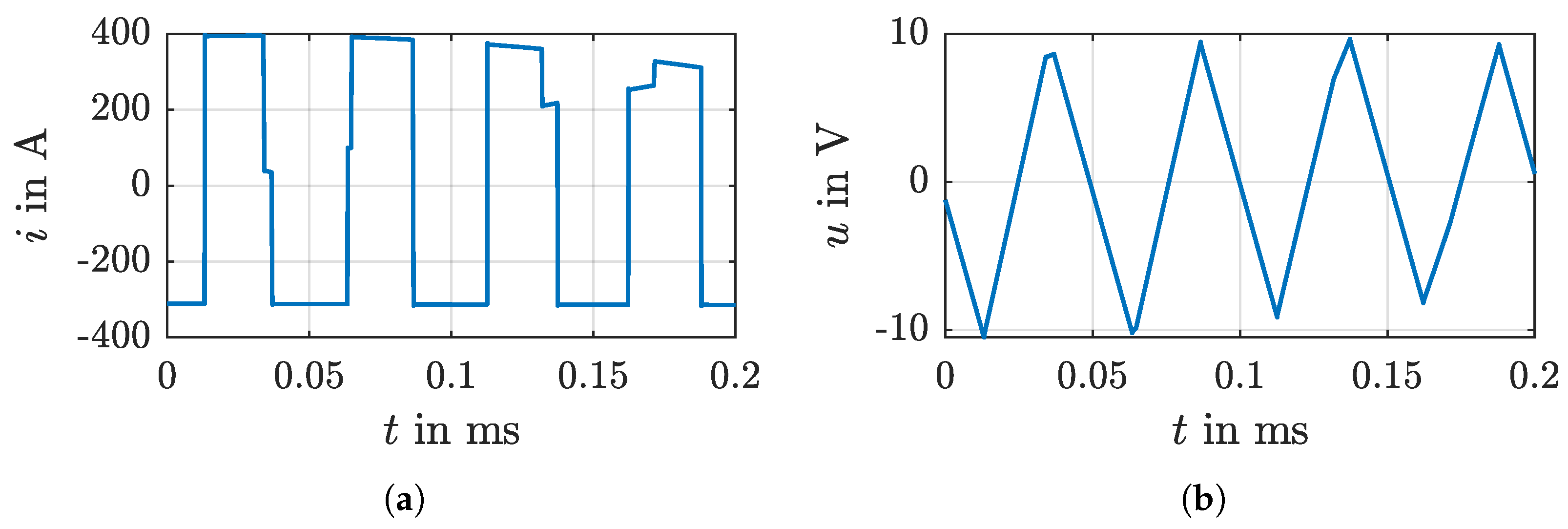
3.3. Time-Based Simulation Model Step I

Using a discrete-time model of the modulator, the DC-side current ripple i E of the VSC is defined according to (1). Equation (2) states that the DC-side current ripple for the top switch, i E , T n (with n representing the phases U, V, and W, respectively) is divided into the top switches’ transistor currents i E , tT n and their diode currents i E , dT n . Equations (3) and (4) calculate the DC-side current ripple for the top switch i E , T n and for the bottom switch i E , B n , respectively. s n represents the switching commandos for all three phase legs:
  • s n = + 1 : Top switch of phase leg n on, corresponding bottom switch off.
  • 1 < s n < + 1 : Commutation between top and bottom switches.
  • s n = 1 : Top switch of phase leg n off, corresponding bottom switch on.
As shown in Figure 4, the current sources for i E , T n as well as for i E , B n are ideally interconnected, respectively. This means that for model step I, the DC-side ripple current could be described by one single current source. The division into six different current sources is performed here in view of the more accurate simulation model step II, where this becomes necessary.
The switching behaviour of the power modules is approximated using a PT2s function with damping of 1 (aperiodic borderline case) and natural angular frequency of 5 / t r , with t r being the rise-time of the power modules as stated in the datasheet.
i E = i E , TU + i E , TV + i E , TW i E ( 0 )
i E , T n = i E , tT n + i E , dT n 1 3 i E , n ( 0 )
i E , T n = s n + 1 2 · i n + 1 2 d s n / d t | d s n / d t | + 1 · | i n | 1 3 3 4 2 · I N · m a · cos ( φ )
i E , B n = s n 1 2 · i n + 1 2 d s n / d t | d s n / d t | 1 · | i n | 1 3 3 4 2 · I N · m a · cos ( φ )
Figure 4 shows the diagram of the model for the three-phase system. The signal s n relates to the switching signals of the half-bridges. Capacitors are simulated by an RLC series resonant circuit. This is sufficient as long as the influence of skin and proximity effects as well as eddy current effects is negligible. Otherwise, more complex models need to be applied [42].
Figure 5 shows simulation results for the time-based simulation model step I. The pulsed DC-side current i E is filtered by the LF filter capacitor, which results in the remaining voltage ripple u RC 1 . As there is no HF filter, the voltage ripple u C 1 shows high-frequency peaks with high amplitude which are neither calculated exactly nor considered in this design step. The simulation was carried out for the operating point with maximum current load at the LF filter capacitor when the analytic calculations are m a = 0 , 6 , φ = 0 ° and f S = 10 kHz . The RMS value of i C 1 over one fundamental period is 325 A , which exactly fits the analytic calculation for this operating point. The RMS value of u RC 1 is 5.6 V here. Although this operating point creates the maximum current load on the filter capacitor, the maximum voltage ripple according to the analytic calculations is reached for m a = 1.15 , φ = 90 ° , and f S = 10 kHz .

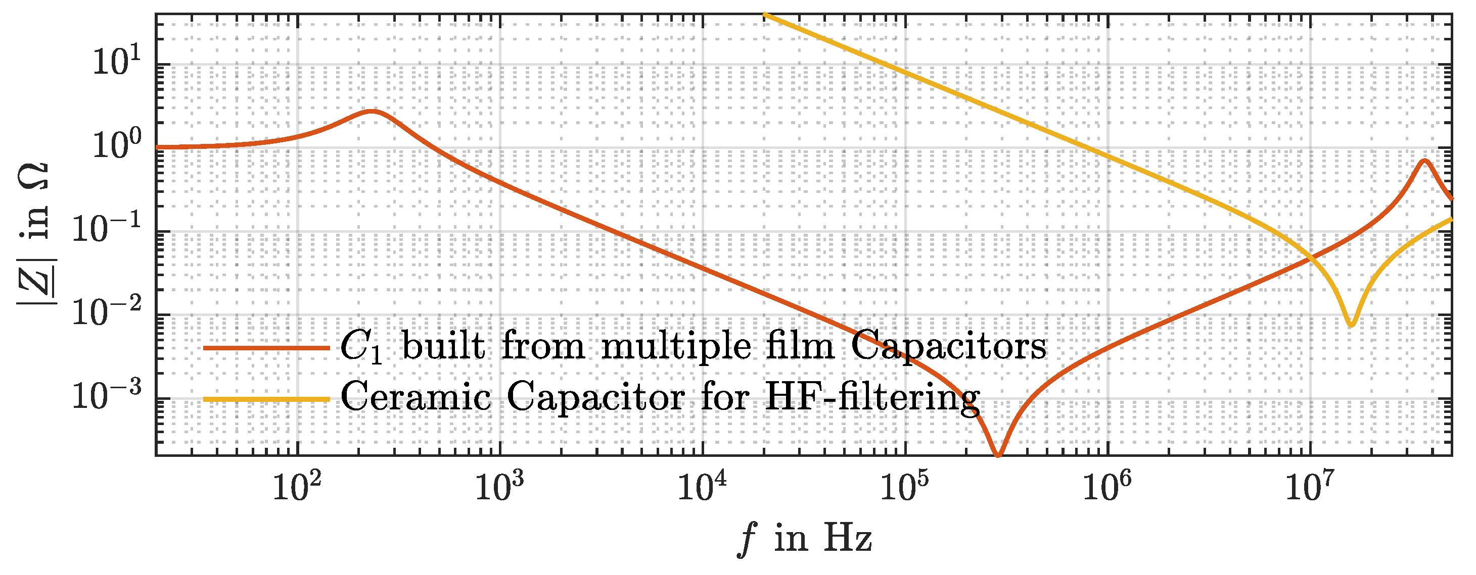
3.4. Component Selection for HF Filter

For HF filtering, switching speed ( d i E / d t ) is more relevant as it strongly influences the HF part of i E . Comparing the amplitude spectrum of i E from Figure 2 with the chosen capacitor impedance (C) shown in Figure 3 indicates that filter performance needs to be improved for f > 1 MHz . Therefore, ceramic capacitors with a series resonance frequency of 15 MHz are installed as close to the power modules as possible. In Figure 6, the impedance of one of these HF filter capacitors is compared to the chosen variant (C) for the LF filter. As can be seen, to significantly improve the filter performance for f > 1 MHz , multiple of these HF filter capacitors are necessary.

3.5. Determine Impedance of Mechanical Components

Mechanical components like PCBs and busbars are necessary for electric connection and mounting of the filter components. This primarily introduces additional inductance in the DC link. Therefore, for a more reliable simulation, the parasitics introduced by the mechanical parts need to be considered. A field solver calculates the electrical parameters of the mechanical parts. Available commercial tools offer front-ends which simplify familiarisation with this topic. Here, a field solver using the boundary method is used. Using the boundary method, radiated emissions are neglected, and so no boundary conditions have to be set. On the other hand, this means the results become inaccurate when the radiated emission reaches relevant levels. As a rule of thumb, it can be stated that the wavelength of the maximum representable frequency should be greater than ten times the dimension of the simulated geometry. Care must be taken when placing the sinks and sources in the field solver tool to ensure that the current loops are considered correctly, as this has influence on the mutual inductance calculated. The results are implemented in the time-based simulation model step II.

3.6. Integration in Time-Based Simulation Model

Applying all the information gathered in Section 3.4 and Section 3.5 to the time-based simulation model results in the diagram shown in Figure 7. It allows determination of the current load on all components and switching voltage overshoot at any places relevant outside the power module. It takes into account the additional stray inductance due to the mechanical structure and the HF filter components. As the impedances of mechanical parts are determined by field solvers, this results in a grey-box model. This approach is also used successfully in the literature, as on the one hand the load on individual components can be determined and on the other hand it offers an efficient method for taking into account parasitic effects of mechanical components [50].
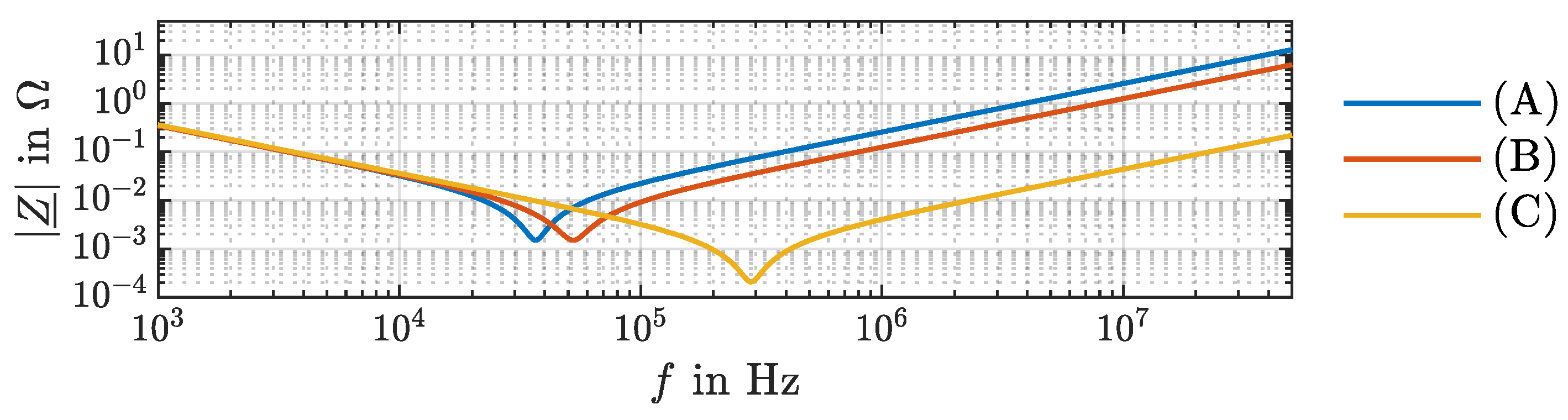
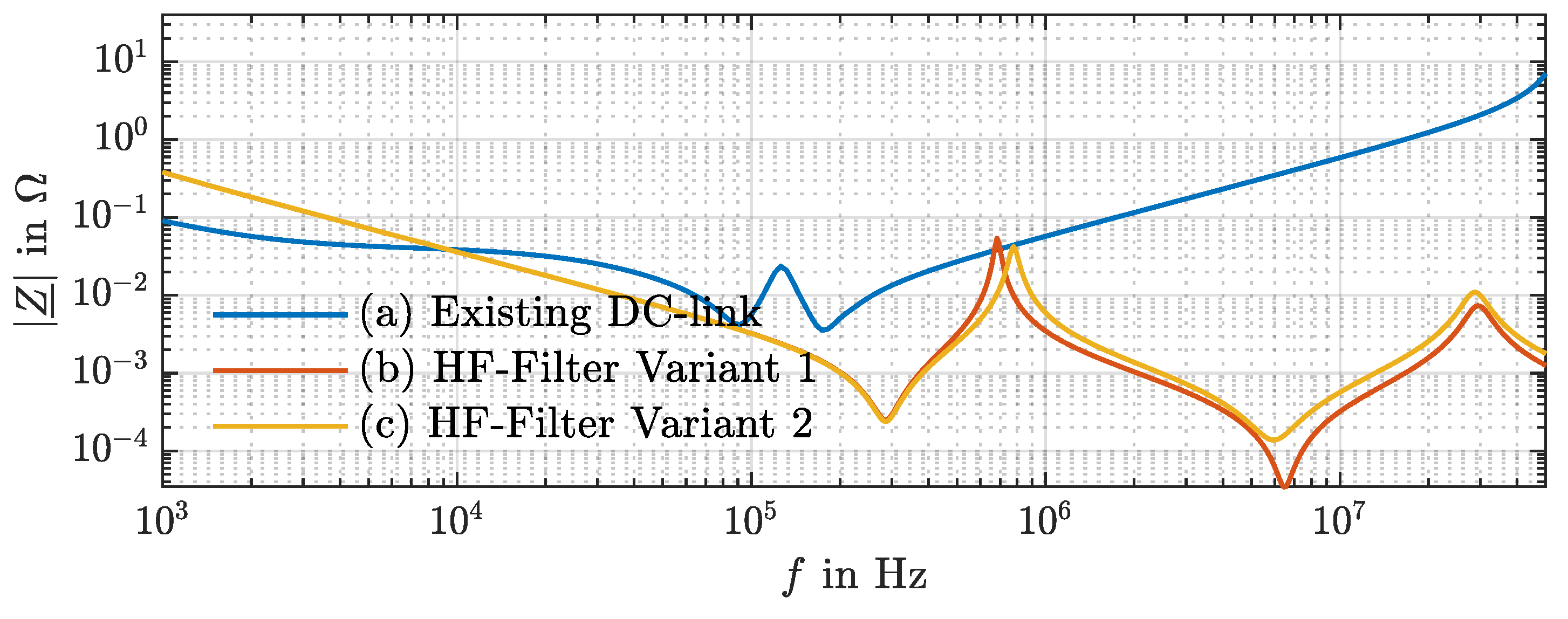
  • Results for different HF filter configurations:
As the model is built from linear components, a linear analysis of the model is possible. Figure 8 shows the input impedance for the old, existing filter concept as well as the design result using the presented approach. Additionally, two different configurations of the HF filter capacitors are compared:
(a)
Existing DC link: HF filter consists of six film capacitors close to the half-bridge power modules. LF filter is built from electrolyte capacitors.
(b)
HF Filter Variant 1: 78 ceramic capacitors are close to the half-bridge power modules.
(c)
HF Filter Variant 2: 60 ceramic capacitors are set in series with low-inductance resistors for damping resonances.
To cope with requirements of insulation coordination, two ceramic capacitors have to be put in series, respectively. With the PCB as a carrier for all the HF filter capacitors, a low-inductive connection of the half-bridges of 4 nH could be realised. Comparing (a) and (b) in Figure 8 determines the improvement in high-frequency filter efficiency introduced by the new filter concept. The new filter concept, variant (b), shows a series resonance at approximately 7 MHz . The time-based model shows that this resonance leads to relatively high current load on the ceramic capacitors. For variant (c), this current load is reduced as described before. It can also be seen by looking at Figure 8.
For quantification, time-based simulations are carried out. The simulation was carried out for an AC-side phase current of 50 A at a switching frequency of 10 kHz and a modulation level of 0.6. The results are stated in Table 2. As the existing DC link uses different types and numbers of capacitors compared to the presented new approach, a comparison of current load on the single capacitors is not applicable for variant (a).
For the maximum AC RMS current of 500 A, the values stated in Table 2 are about 10 times higher. The results quantify the improved HF filter performance of the new approach compared to the existing DC link. As can be seen, configuration (c) makes a compromise between voltage overshoot and current load on the filter components.

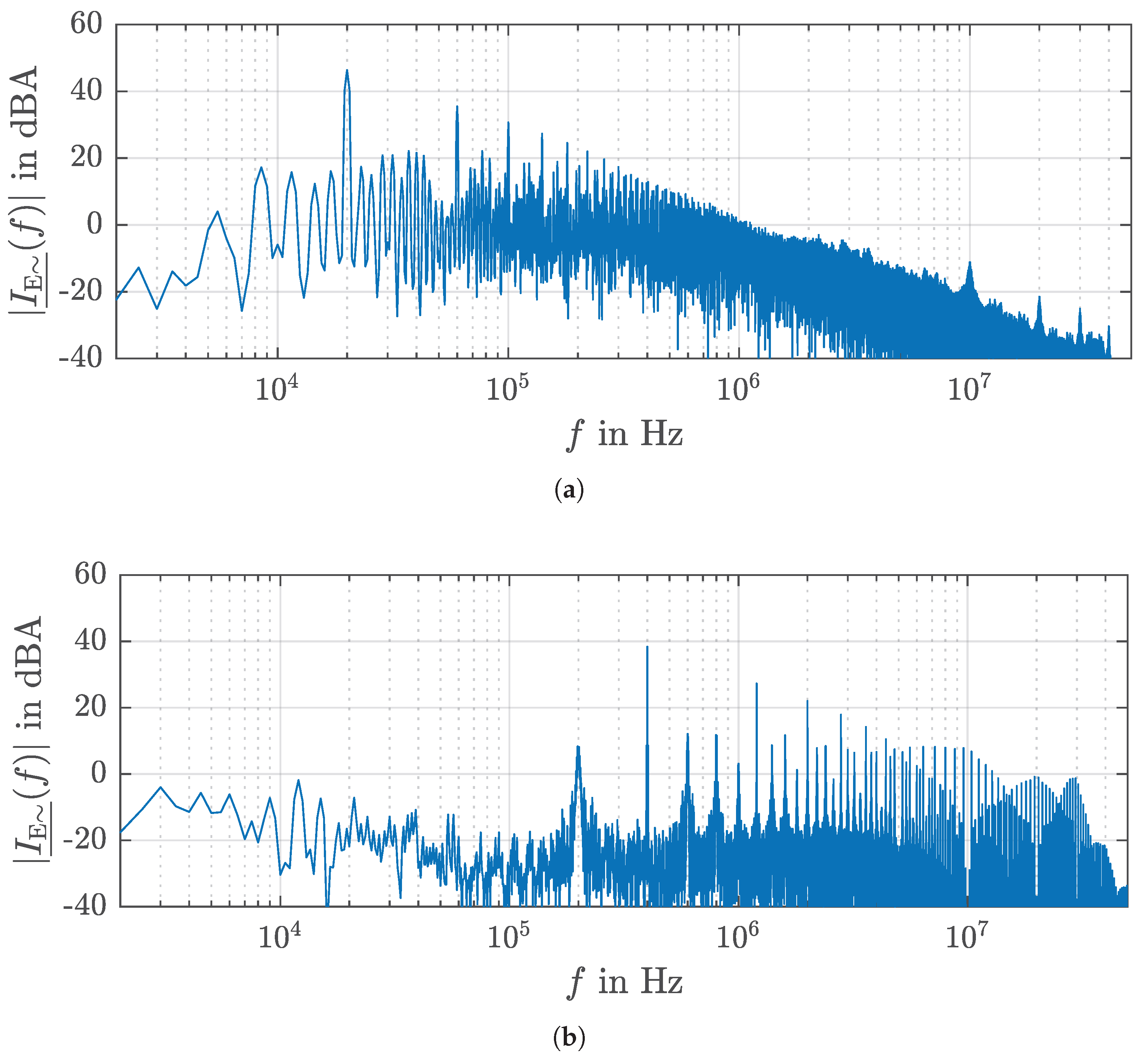
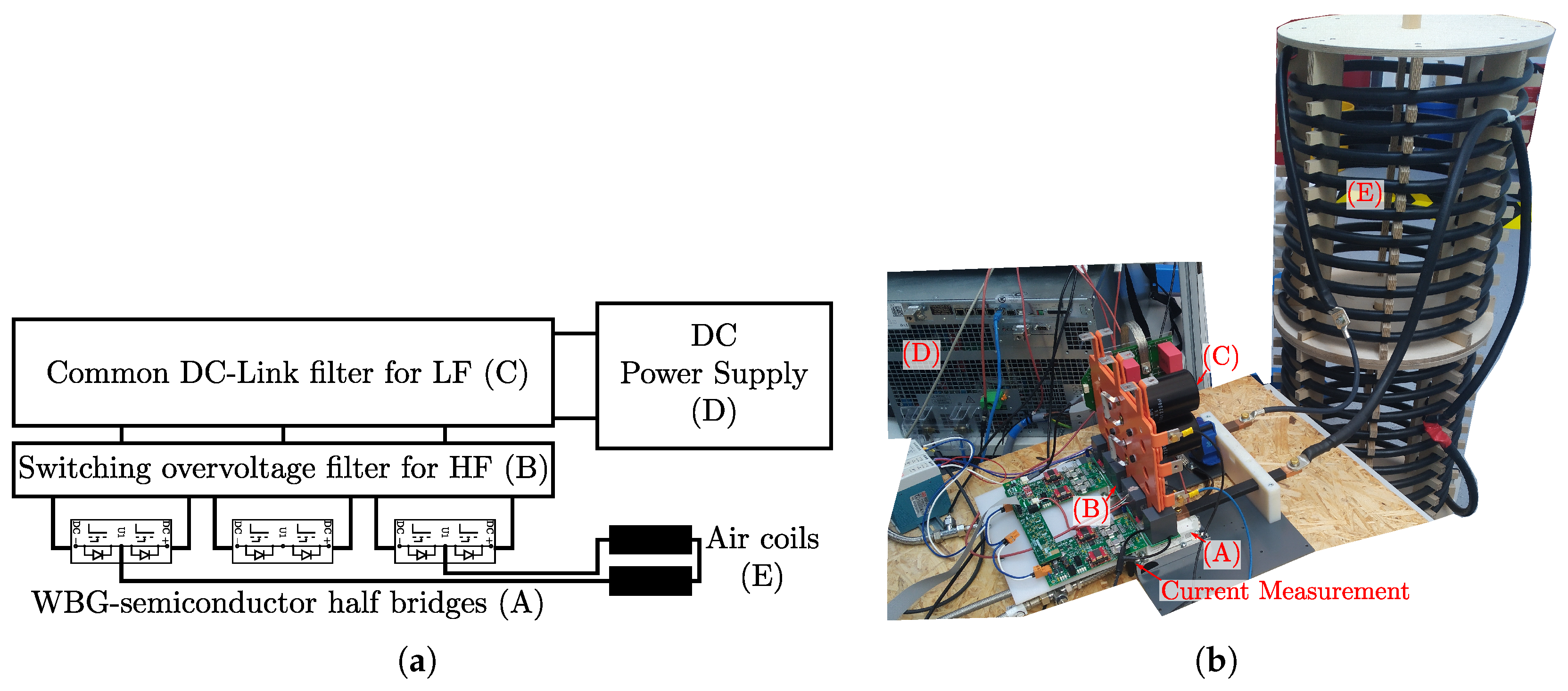
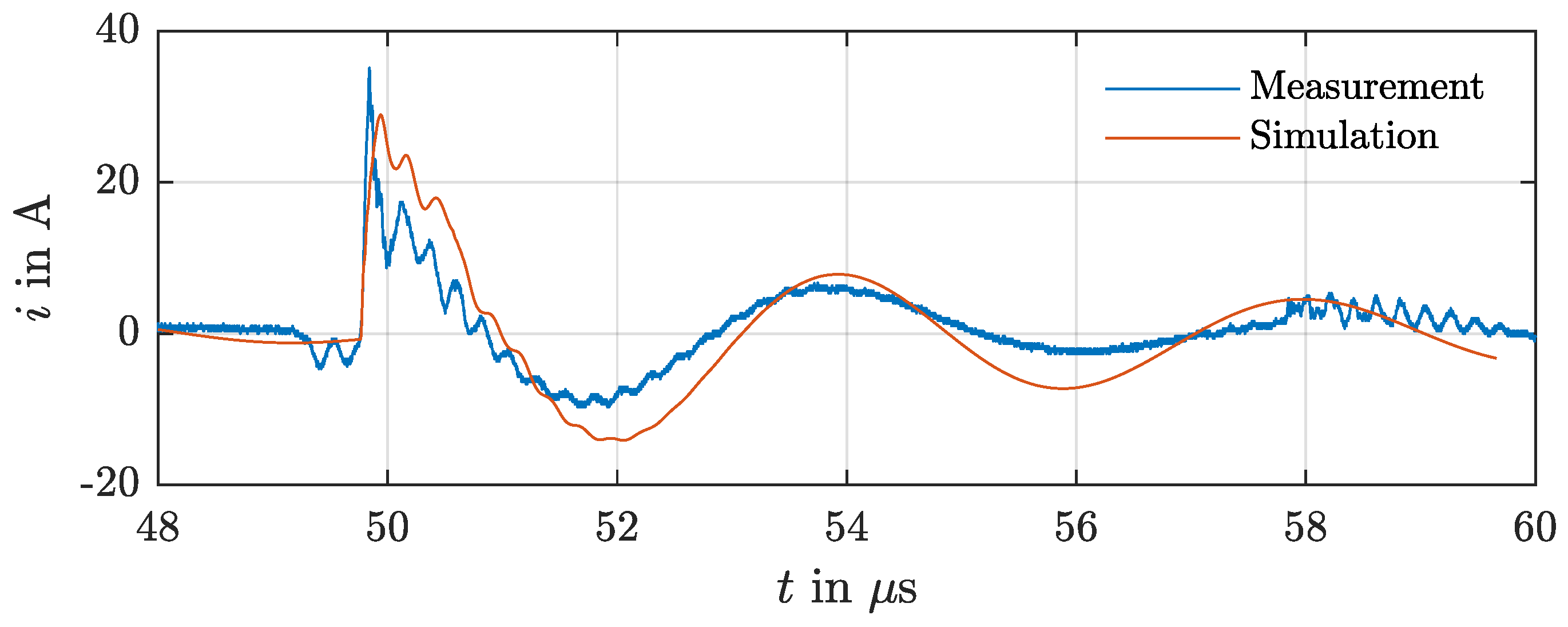
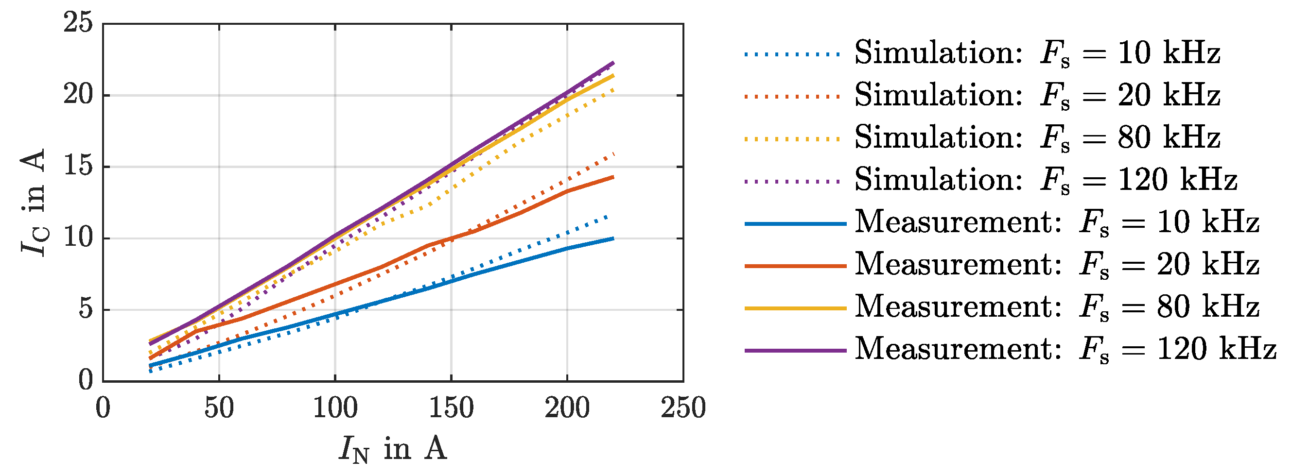
4. Validation of Simulation Model

For validation of the model, measurements were made on an experimental setup. It is presented in Figure 9.
Air coils are connected between the mid-points of the half-bridges for phases U and W, respectively, as AC-side load and the VSC is operated like a full-bridge converter. The VSC is powered via a DC power supply. As the newly designed filter variants (b) and (c) do not exist yet, the existing filter variant (a) is used here. To measure the current load of one of the film capacitors, a rogowski coil was used. It has an HF bandwidth of 30 MHz and can measure a maximum current rise of 2 kA / μ s . The current rise measured in the setup was 0.5 kA / μ s .
Figure 10 shows the results for both measurement and simulation at an identical operating point of the VSC. It can be seen that there is good agreement.
Further validation is performed for different operating points. Table 3 shows the simulation as well as the measurement results for different AC-side RMS currents. The VSC is operated at a fixed switching frequency of 10 kHz. The results show good agreement for 60 A I N 200 A . For I N 60 A , accuracy of the measurement equipment comes into consideration with 0.41 A for I N = 20 A ( 2 % of reading for conductor position and 0.05 % of reading for linearity error). For I N = 220 A , the maximum capable current of the rogowski coil used is reached.
Additionally, Figure 11 shows the comparison for different switching frequencies F s . It can be seen that the method presented shows valid results also for different switching frequencies. Table 4 shows the relative error for the different operating points and switching frequencies from Figure 11. The deviations between simulation and measurement are in the same range for the different switching frequencies.

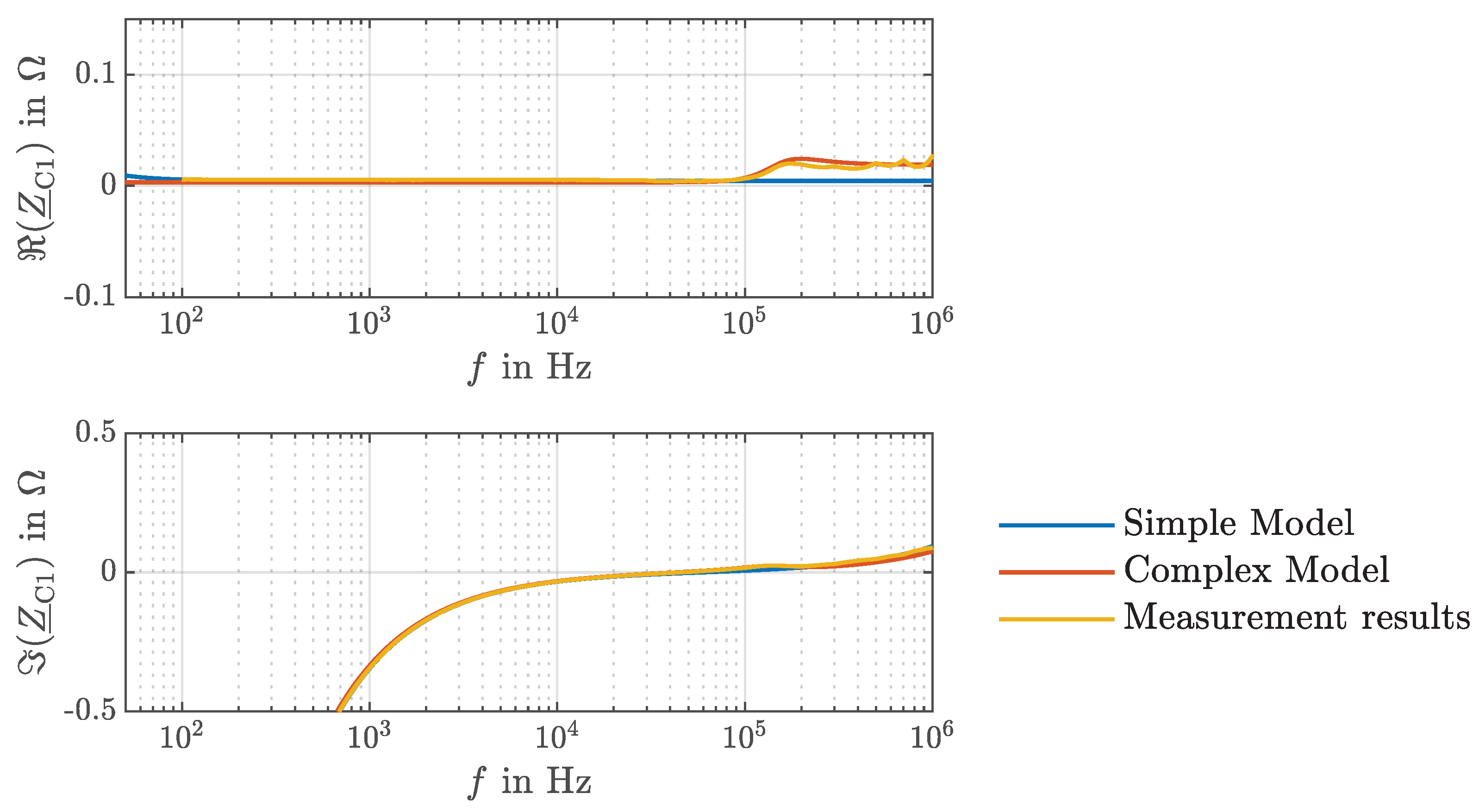
5. Non-Linear Loss Effects in Film Capacitors

In Figure 12a, a simple capacitor model is shown. It takes into account the voltage drop at the ESR of the capacitor and parasitic, voltage-dependent losses. The skin and proximity losses of the capacitor are taken into account by the inductance L C 1 representing the ESL of the capacitor. The series connection of L C 1 and C 1 forms a series resonant circuit whose resonance condition is specified in Equation (5). The frequency at which the series resonance occurs is called the series resonance frequency f SR .
1 ω C 1 = ω L C 1 for ω = ω SR = 2 π f SR | R C 1 , P > > 1 ω SR C 1
The limits of the influence of L C 1 on the HF behaviour of the capacitor impedance and the need to implement further elements in the component model are discussed below. For this purpose, the result of an impedance measurement is presented. The measurement was carried out using a vector network analyser. Capacitor (A) from Figure 3 is measured here. To illustrate the effects of the observed phenomenon, real and imaginary parts of the measurement result are determined. These are presented in Figure 13. From the diagram it can be seen that the real part of the measured impedance increases for 100 kHz f 200 kHz . The result for the simple model (Figure 12a) does not show this behaviour. Instead, the complex model (Figure 12b) addresses this effect.
The measured behaviour of the impedance is adequately described in the literature and can be attributed to the following phenomena, which are not sufficiently described by means of ESL [37]:
  • Skin effect;
  • Proximity effect;
  • Eddy currents.
The cause of these phenomena is attributed to the magnetic fields generated at high frequencies in the windings of the capacitor [39,51]. The result of these magnetic fields are eddy currents which influence the current density distribution within the capacitor. This leads to impedance fluctuations and resonance effects at certain frequencies, whose position also depends on the geometry of the capacitor. Especially in the range of the capacitors’ resonance frequencies, a considerable increase in the ohmic internal resistance is expected. The visible consequence of this is the occurrence of local heating [41]. To take into account the named phenomena, according to [42], the model can be enhanced as follows:
1.
To map skin and proximity losses within the capacitor, the inductance at L C 1 mapping the ESL is substituted. The skin losses are represented by a first-order high-pass filter consisting of the resistor R C 1 , Skin and the inductance L C 1 , Skin . To account for the proximity losses, the inductance L C 1 , Prox is also implemented in the capacitor model.
2.
To represent the eddy currents and the additional losses caused by them, a second-order high-pass filter (parallel dipole) consisting of the inductance L C 1 , AR , the resistance R C 1 , AR , and the capacitance C 1 , AR is implemented in the capacitor model.
The resulting model, addressing all these effects, is shown in Figure 12b. In the following, the equivalent circuit data of this model are determined. The parametrisation of the model is carried out in an exemplary fashion on the basis of the measurement results of the experimental setup generated by means of the network analyser.
The parameters of R C 1 , Skin , L C 1 , Skin , and L C 1 , Prox are determined based on the measurement results. In (7), the real and imaginary parts of Z ̲ C 1 are given. The values for the real and imaginary parts are taken directly from the measurement. They are chosen for f > 500 kHz to avoid the influence of the rapid increase in the real part introduced by eddy currents. In addition, the context given in (6) is applied.
L C 1 = L C 1 , Skin + L C 1 , Prox
The component values can be calculated by inserting the measured values for the real and imaginary parts as well as (6) into (7). If the resulting equations have more than one solution, the physically most sensible solution is chosen.
( Z ̲ C 1 ) = R C 1 , S + R C 1 , P C 1 2 R C 1 , P 2 ω 2 + 1 + L C 1 , Skin 2 R C 1 , Skin ω 2 L C 1 , Skin 2 ω 2 + R C 1 , Skin 2 ( Z ̲ C 1 ) = L C 1 , Prox · ω C 1 R C 1 , P 2 ω C 1 2 R C 1 , P 2 ω 2 + 1 + L C 1 , Skin R C 1 , Skin 2 ω L C 1 , Skin 2 ω 2 + R C 1 , Skin 2
Also shown in Figure 12 is the high pass formed by C 1 , AR , L C 1 , AR , and R C 1 , AR . This element is mainly relevant to address the rapid increase in the real part. The equivalent circuit diagram data of the high-pass filter are determined from the frequency response of the real part of the measurement result. The criteria taken from the measurement are the quality Q AR and and the resonant angular frequency ω R , AR . Here, Q AR = 1 , 1 and ω R , AR = 150 · 10 3 rad / s was chosen. For R C 1 , AR the following applies:
R C 1 , AR = ( Z ̲ C 1 ( ω R , AR ) )
For the Q AR and ω R , AR results,
Q AR = 1 R C 1 , AR L C 1 , AR C AR
ω R , AR = 1 L C 1 , AR C AR
L C 1 = L C 1 , AR + L C 1 , SP
By converting (9) and (10) to C AR , C AR can first be substituted and L AR can be calculated. Then C AR can also be determined using (9) or (10).
The qualitative comparison between the simple model, the complex model, and the measurement results shows the better fitting of the complex model to the measured results. Especially when looking at the real parts, clear differences are noticeable between the simple model and the measurement results, which mean inaccurate representation of the capacitors’ high-frequency losses. As the complex model consists only of linear components, calculation effort during the simulation is not much higher compared to the simple model.

6. Discussion

This paper describes a simulation-based design methodology for the DC link filter of WBG-based VSCs. The methodology is described using an example of a three-phase VSC. Validation shows that moderate model precision can be reached with only a few iterative steps. The model enables us to determine the current load on the individual components, which is often not measurable in the real application. This allows faster and more precise design of the DC link especially for fast-switching WBG devices where HF filtering becomes crucial. Nevertheless, a model validation on an experimental setup is obligatory, as not all effects are considered in the model approach, including the following:
  • Temperature and current dependent behaviour;
  • Production-related component tolerances;
  • Resonances occurring in the composite system.
Implementation of these effects should be considered only if necessary, as it may significantly increase the computing time of the models and influence the convergence of the solver. The necessity can be determined by experimental validation.
Furthermore, this paper describes briefly what parasitic effects influence a DC link capacitor’s filter efficiency and how they can be taken into account in the model.
  • Model restrictions:
Usually, VSCs are not controlled via setting a defined set-point sine wave for the modulator. Instead, a superimposed control structure, for example, a PI current controller, is used to adjust the modulator’s set point in such way that the set-point current is applied to the load. To focus on the objective here, the influence of this feedback loop is neglected in the structure shown in Figure 7. Figure 14 now shows the measured and the simulated amplitude spectrum | I ̲ C | of the capacitor load current i C for I N = 220 A, f s = 80 kHz and f 1 = 100 Hz. Although on the test-bench, a superimposed PI current controller is used to adjust the set-point, the simulation is only controlled in a feedforward manner. It can be seen from the results that in the case under consideration, the odd harmonics (mainly first, third, and fifth) of the switching frequency are especially influenced by the superimposed controller, which is the main reason for the deviations between simulation and measurement. This means that simulation results could be improved by including the superimposed controllers. But on the other hand, this would result in a significantly more complex simulation model, as the AC-side load circuit, measurement data processing, and digital controllers need to be added to the model.
Not implementing the superimposed control structure also means that dynamic processes like load changes cannot be simulated exactly as the systems control dynamic is neglected. The model is intended to determine the load current for all quasi-stationary operating points that occur in real-life operation. Other modelling approaches briefly describe the HF behaviour [19]. In real hardware, various hardware-specific effects like the non-linear behaviour of the transistor output capacitance cause high-frequency oscillations [52,53,54,55]. These effects influence switching losses, especially when high switching frequencies (in the MHz range) are introduced [56]. The goal of the approach mentioned in this paper is mainly to have a design tool for engineers to estimate their DC link capacitor current load and the remaining voltage overshoot, which are two crucial factors for DC link filter design. Therefore, a trade-off was made between the model accuracy and the practical usability for design engineers, who often do not have access to such specific information like the non-linear behaviour of the transistor output capacitance.
  • Higher switching frequencies
Figure 15 shows the measured amplitude spectrum | I ̲ C | of the capacitor load current i C for I N = 40 A, f s = 200 kHz and f 1 = 100 Hz. The deviation especially of the first harmonic amplitude is higher than in Figure 14, although it is for the same reason. It is related to the superimposed PI controller not taken into account in the simulation model. It is observed that the deviation becomes more for higher switching frequencies, as the controller reacts to switching noise and forces unnecessary switching actions that generate additional DC-side ripple current. This could be improved by using a more sophisticated superimposed controller.

7. Future Development

Deviations between simulation and measurement can also be seen in Figure 14, looking at the frequency range from 2 MHz to 10 MHz. The amplitude spectrum generated by simulation starts decreasing for frequencies higher than 3 MHz, while in the measurement it starts decreasing at about 5.6 MHz. This deviation comes from an inaccuracy in the simulation of the switching behaviour of the semiconductor switches. It is approximated using a PT2s function with a damping of 1, as described in Section 3.3. This is a very simple method that saves computational effort and that does not need too much specific information about the semiconductor. But as these high-frequency amplitudes resulting from the switching behaviour can stimulate resonances in the DC filter, a more precise simulation of the switching behaviour is desirable. This will be part of future developments.

Author Contributions

Conceptualisation and methodology: S.R.; validation: S.W. and S.R.; formal analysis: H.K.; writing—original draft preparation: S.R.; writing—review and editing: S.W. and H.K.; supervision: H.K. All authors have read and agreed to the published version of the manuscript.

Funding

This work has been carried out in the framework of the European Project GaN4AP (Gallium Nitride for Advanced Power Applications). The project has received funding from the Electronic Component Systems for European Leadership Joint Undertaking (ECSEL JU), under grant agreement No. 101007310. This Joint Undertaking receives support from the European Union’s Horizon 2020 research and innovation programme, and Italy, Germany, France, Poland, Czech Republic, The Netherlands.

Data Availability Statement

The raw data supporting the conclusions of this article will be made available by the authors on request.

Conflicts of Interest

The authors declare no conflicts of interest.

Abbreviations

The following abbreviations are used in this manuscript:
DCDirect current
VSCVoltage source converter
DMDifferential mode
HFHigh frequency
WBGWide bandgap
SVMSpace vector modulation
MPPFCMetallised polypropylene film capacitor
ESLEquivalent Series Inductance
ESREquivalent Series Resistance

References

  1. Kolar, J.W.; Round, S.D. Analytical calculation of the RMS current stress on the DC-link capacitor of voltage-PWM converter systems. IEEE Proc.—Electr. Power Appl. 2006, 153, 535. [Google Scholar] [CrossRef]
  2. Dahono, P.A.; Sato, Y.; Kataoka, T. Analysis and minimization of ripple components of input current and voltage of PWM inverters. IEEE Trans. Ind. Appl. 1996, 32, 945–950. [Google Scholar] [CrossRef]
  3. Holmes, D.G. A general analytical method for determining the theoretical harmonic components of carrier based PWM strategies. In Proceedings of the Conference Record of 1998 IEEE Industry Applications Conference. Thirty-Third IAS Annual Meeting, St. Louis, MO, USA, 12–15 October 1998; pp. 1207–1214. [Google Scholar] [CrossRef]
  4. Huang, X.; Lai, J.-S.; Pepa, E. Analytical evaluation of modulation effect on three-phase inverter differential mode noise prediction. In Proceedings of the Nineteenth Annual IEEE Applied Power Electronics Conference and Exposition, 2004. APEC ’04, Anaheim, CA, USA, 22–26 February 2004; pp. 681–687. [Google Scholar] [CrossRef]
  5. Hava, A.M.; Kerkman, R.J.; Lipo, T.A. Simple analytical and graphical tools for carrier based PWM methods. In Proceedings of the PESC97. Record 28th Annual IEEE Power Electronics Specialists Conference. Formerly Power Conditioning Specialists Conference 1970–1971. Power Processing and Electronic Specialists Conference 1972, St. Louis, MO, USA, 22–27 June 1997; pp. 1462–1471. [Google Scholar] [CrossRef]
  6. Un, E.; Hava, A.M. Performance Analysis and Comparison of Reduced Common Mode Voltage PWM and Standard PWM Techniques for Three-Phase Voltage Source Inverters. In Proceedings of the Twenty-First Annual IEEE Applied Power Electronics Conference and Exposition, 2006. APEC ’06, Dallas, TX, USA, 19–23 March 2006; pp. 303–309. [Google Scholar] [CrossRef]
  7. Hava, A.M.; Kerkman, R.J.; Lipo, T.A. Simple analytical and graphical methods for carrier-based PWM-VSI drives. IEEE Trans. Power Electron. 1999, 14, 49–61. [Google Scholar] [CrossRef]
  8. Gu, B.G.; Nam, K. A DC-link capacitor minimization method through direct capacitor current control. IEEE Trans. Ind. Appl. 2006, 42, 573–581. [Google Scholar] [CrossRef]
  9. Welchko, B.A. Analytical calculation of the RMS current stress on the DC link capacitor for a VSI employing reduced common mode voltage PWM. In Proceedings of the 2007 European Conference on Power Electronics and Applications, Aalborg, Denmark, 2–5 September 2007; IEEE: Piscataway, NJ, USA, 2007. [Google Scholar] [CrossRef]
  10. Un, E.; Hava, A.M. A Near-State PWM Method with Reduced Switching Losses and Reduced Common-Mode Voltage for Three-Phase Voltage Source Inverters. IEEE Trans. Ind. Appl. 2009, 45, 782–793. [Google Scholar] [CrossRef]
  11. Hava, A.M.; Ün, E. A High-Performance PWM Algorithm for Common-Mode Voltage Reduction in Three-Phase Voltage Source Inverters. IEEE Trans. Power Electron. 2011, 26, 1998–2008. [Google Scholar] [CrossRef]
  12. Nguyen, T.D.; Patin, N.; Friedrich, G. PWM strategy dedicated to the reduction of DC bus capacitor stress in embedded three phase inverter. In Proceedings of the 2011 IEEE Vehicle Power and Propulsion Conference, Chicago, IL, USA, 6–9 September 2011. [Google Scholar] [CrossRef]
  13. Cetin, N.O.; Hava, A.M. Topology and PWM method dependency of high frequency leakage current characteristics of voltage source inverter driven AC motor drives. In Proceedings of the 2012 IEEE Energy Conversion Congress and Exposition (ECCE), Raleigh, NC, USA, 15–20 September 2012; pp. 3430–3437. [Google Scholar] [CrossRef]
  14. Cao, W.; Wang, F.; Jiang, D. Variable switching frequency PWM strategy for inverter switching loss and system noise reduction in electric/hybrid vehicle motor drives. In Proceedings of the 2013 Twenty-Eighth Annual IEEE Applied Power Electronics Conference and Exposition (APEC), Long Beach, CA, USA, 17–21 March 2013. [Google Scholar] [CrossRef]
  15. Sommer, C.; Merkert, A.; Mertens, A. A new control method for minimizing the DC-link capacitor current of HEV inverter systems. In Proceedings of the 2014 IEEE Energy Conversion Congress and Exposition (ECCE), Pittsburgh, PA, USA, 14–18 September 2014. [Google Scholar] [CrossRef]
  16. Basler, B.; Greiner, T.; Heidrich, P. Reduction of DC link capacitor stress for double three-phase drive unit through shifted control and phase displacement. In Proceedings of the 2015 IEEE 11th International Conference on Power Electronics and Drive Systems, Sydney, NSW, Australia, 9–12 June 2015; pp. 887–889. [Google Scholar] [CrossRef]
  17. Berlinecke, J.; Henke, M.; Plikat, R. Ansteuerverfahren multiphasiger E-Antriebe–Simulation und Bewertung von Raumzeigermodulationen. In Proceedings of the 10. Tagung Elektrische Antriebstechnologie für Hybrid- und Elektrofahrzeuge, Würzburg, Deutschland, 27 September 2017. [Google Scholar]
  18. Lamp, J. IGBT Peak Voltage Measurement and Snubber Capacitor Specification; Semikron: Singapore, 2008. [Google Scholar]
  19. Zhao, S.; Zhang, M.; Zhang, Z.; Zhu, N.; Zhao, Y.; Li, H.; Ding, L. Analytic Model of the Voltage Oscillation in a High-Power Converter with Silicon Carbide Devices. IEEE Trans. Ind. Appl. 2024, 60, 3345–3358. [Google Scholar] [CrossRef]
  20. Babaki, A.; Golsorkhi, M.S.; Christensen, N.; Baharizadeh, M.; Behrendt, S.; Beyer, J.; Ebel, T. Parasitic-Based Model for Characterizing False Turn-On and Switching-Based Voltage Oscillation in Hybrid T-Type Converter. Electronics 2024, 13, 1808. [Google Scholar] [CrossRef]
  21. Liu, Q.; Wang, S.; Baisden, A.; Wang, F.; Boroyevich, D. EMI Suppression in Voltage Source Converters by Utilizing dc-link Decoupling Capacitors. IEEE Trans. Power Electron. 2007, 22, 1417–1428. [Google Scholar] [CrossRef]
  22. Schulting, P.; Kubon, D.; De Doncker, R.W. Electrical design considerations for a 4 kW buck converter with normally-off GaN devices at a Dc-link voltage of 400 V. In Proceedings of the 2016 IEEE 2nd Annual Southern Power Electronics Conference (SPEC), Auckland, New Zealand, 5–8 December 2016; pp. 1–6. [Google Scholar] [CrossRef]
  23. Stewart, J.; Neely, J.; Delhotal, J.; Flicker, J. DC link bus design for high frequency, high temperature converters. In Proceedings of the 2017 IEEE Applied Power Electronics Conference and Exposition (APEC), Tampa, FL, USA, 26–30 March 2017; pp. 809–815. [Google Scholar] [CrossRef]
  24. Wang, F.; Zhang, Z.; Ericsen, T.; Raju, R.; Burgos, R.; Boroyevich, D. Advances in Power Conversion and Drives for Shipboard Systems. Proc. IEEE 2015, 103, 2285–2311. [Google Scholar] [CrossRef]
  25. Laird, I.; Yuan, X.; Scoltock, J.; Forsyth, A.J. A Design Optimization Tool for Maximizing the Power Density of 3-Phase DC–AC Converters Using Silicon Carbide (SiC) Devices. IEEE Trans. Power Electron. 2018, 33, 2913–2932. [Google Scholar] [CrossRef]
  26. Parvez, M.; Pereira, A.T.; Ertugrul, N.; Weste, N.H.E.; Abbott, D.; Al-Sarawi, S.F. Wide Bandgap DC–DC Converter Topologies for Power Applications. Proc. IEEE 2021, 109, 1253–1275. [Google Scholar] [CrossRef]
  27. Forte, G.; Spampinato, A. High Power-Density Design Based on WBG GaN Devices for Three-Phase Motor Drives. In Proceedings of the 2024 International Symposium on Power Electronics, Electrical Drives, Automation and Motion (SPEEDAM), Napoli, Italy, 19–21 June 2024; pp. 65–70. [Google Scholar] [CrossRef]
  28. Nasrin, M.S.; Khan, F.H.; Alam, M.K. Quantifying Device Degradation in Live Power Converters Using SSTDR Assisted Impedance Matrix. IEEE Trans. Power Electron. 2014, 29, 3116–3131. [Google Scholar] [CrossRef]
  29. Wang, H.; Blaabjerg, F. Reliability of Capacitors for DC-Link Applications in Power Electronic Converters - An Overview. IEEE Trans. Ind. Appl. 2014, 50, 3569–3578. [Google Scholar] [CrossRef]
  30. Novák, I. DC and AC Bias Dependence of Capacitors. In Proceedings of the DesignCon, Santa Clara, CA, USA, 27 September 2011. [Google Scholar]
  31. Sullivan, C.; Sun, Y.; Kern, A. Improved distributed model for capacitors in high-performance packages. In Proceedings of the Conference Record of the 2002 IEEE Industry Applications Conference. 37th IAS Annual Meeting (Cat. No.02CH37344), Pittsburgh, PA, USA, 13–18 October 2002. [Google Scholar] [CrossRef]
  32. Tyshko, A.; Balevicius, S. Specifics of the X7R capacitors application in the high frequency inverters. In Proceedings of the 2016 IEEE 36th International Conference on Electronics and Nanotechnology (ELNANO), Kyiv, Ukraine, 19–21 April 2016. [Google Scholar] [CrossRef]
  33. Coday, S.; Barth, C.B.; Pilawa-Podgurski, R.C. Characterization and Modeling of Ceramic Capacitor Losses under Large Signal Operating Conditions. In Proceedings of the 2018 IEEE 19th Workshop on Control and Modeling for Power Electronics (COMPEL), Padua, Italy, 25–28 June 2018. [Google Scholar] [CrossRef]
  34. Haag, H.; Haemmerle, F.; Ben-Yaakov, S. Voltage Bias Effect on the ESR of Ferroelectric Ceramic Capacitors. In Proceedings of the PCIM Europe digial days 2020 International Exhibition and Conference for Power Electronics, Intelligent Motion, Renewable Energy and Energy Management Proceedings, Berlin, Germany, 7–8 July 2020. [Google Scholar]
  35. Haag, H.; Mitterbacher, A.; Haemmerle, F. Losses in Ferroelectric Dielectric Ceramic Capacitors due to Electromechanical Resonances. In Proceedings of the PCIM Europe digial days 2020 International Exhibition and Conference for Power Electronics, Intelligent Motion, Renewable Energy and Energy Management Proceedings, Berlin, Germany, 7–8 July 2020. [Google Scholar]
  36. Wöhrle, D.; Armbruster, C.; Schöner, C. Design of a Fast Switching 200 kVA SiC Drive Inverter for Aviation Application. In Proceedings of the PCIM Europe 2023; International Exhibition and Conference for Power Electronics, Intelligent Motion, Renewable Energy and Energy Management, Nuremberg, Germany, 9–11 May 2023. [Google Scholar] [CrossRef]
  37. Joubert, C.; Béroual, A.; Rojat, G. Magnetic field and current distribution in metallized capacitors. J. Appl. Phys. 1994, 76, 5288–5293. [Google Scholar] [CrossRef]
  38. Iorga, C. Compartmental analysis of dielectric absorption in capacitors. IEEE Trans. Dielectr. Electr. Insul. 2000, 7, 187–192. [Google Scholar] [CrossRef]
  39. Joubert, C.; Béroual, A.; Rojat, G. Asymmetrical current distribution in metallized film capacitors. J. Appl. Phys. 2004, 95, 6420–6425. [Google Scholar] [CrossRef]
  40. Kundert, K. Modeling Dielectric Absorption in Capacitors; Technical report; Designers Guide Consulting Inc.: Boulder, CO, USA, 2008. [Google Scholar]
  41. Hosking, T. Eddy Current Effects in Film Capacitors and Their Impact on Interconnect Systems in High Power Applications; Technical report, Power Ring Division; SBE Inc.: San Francisco, CA, USA, 2009. [Google Scholar]
  42. Makdessi, M.; Sari, A.; Venet, P. Improved model of metalized film capacitors. IEEE Trans. Dielectr. Electr. Insul. 2014, 21, 582–593. [Google Scholar] [CrossRef]
  43. Li, H.; Huang, X.; Li, Z.; Li, H.; Wang, W.; Wang, B.; Zhang, Q.; Lin, F. Modeling of ESR in metallized film capacitors and its implication on pulse handling capability. Microelectron. Reliab. 2015, 55, 1046–1053. [Google Scholar] [CrossRef]
  44. Wen, H.; Xiao, W.; Wen, X.; Armstrong, P. Analysis and Evaluation of DC-Link Capacitors for High-Power-Density Electric Vehicle Drive Systems. IEEE Trans. Veh. Technol. 2012, 61, 2950–2964. [Google Scholar] [CrossRef]
  45. Zhang, H.; Wheeler, N.; Grant, D. Switching harmonics in the DC link current in a PWM AC-DC-AC converter. In Proceedings of the IAS ’95. Conference Record of the 1995 IEEE Industry Applications Conference Thirtieth IAS Annual Meeting, Orlando, FL, USA, 8–12 October 1995. [Google Scholar] [CrossRef]
  46. Mariscotti, A. Analysis of the DC-link current spectrum in voltage source inverters. IEEE Trans. Circuits Syst. I Fundam. Theory Appl. 2002, 49, 484–491. [Google Scholar] [CrossRef]
  47. Holmes, D.G. Pulse Width Modulation for Power Converters; Wiley-Blackwell: Oxford, UK, 2003. [Google Scholar]
  48. Zhang, D.; Wang, F.; Burgos, R.; Lai, R.; Boroyevich, D. DC-Link Ripple Current Reduction for Paralleled Three-Phase Voltage-Source Converters with Interleaving. IEEE Trans. Power Electron. 2011, 26, 1741–1753. [Google Scholar] [CrossRef]
  49. McGrath, B.; Holmes, D. A General Analytical Method for Calculating Inverter DC-Link Current Harmonics. IEEE Trans. Ind. Appl. 2009, 45, 1851–1859. [Google Scholar] [CrossRef]
  50. Schoerle, S.; Hoene, E.; Lang, K.D. Automotive high voltage grid simulation modelling and simulation high voltage car grids from system prospective. In Proceedings of the 2014 International Symposium on Electromagnetic Compatibility, Gothenburg, Sweden, 1–4 September 2014. [Google Scholar] [CrossRef]
  51. Siami, S.; Joubert, C.; Glaize, C. High frequency model for power electronics capacitors. IEEE Trans. Power Electron. 2001, 16, 157–166. [Google Scholar] [CrossRef]
  52. Yang, X.; Li, J.; Ding, Y.; Xu, M.; Zhu, X.F.; Zhu, J. Observation of Transient Parity-Time Symmetry in Electronic Systems. Phys. Rev. Lett. 2022, 128, 065701. [Google Scholar] [CrossRef]
  53. Yan, D.; Hang, L.; He, Y.; He, Z.; Zeng, P. An Accurate Switching Transient Analytical Model for GaN HEMT under the Influence of Nonlinear Parameters. Energies 2022, 15, 2966. [Google Scholar] [CrossRef]
  54. Duraij, M.; Xiao, Y.; Zsurzsan, G.; Zhang, Z. Switching Performance in a GaN Power Stage at Extreme Temperature Conditions. In Proceedings of the 2021 IEEE 8th Workshop on Wide Bandgap Power Devices and Applications (WiPDA), Redondo Beach, CA, USA, 7–11 November 2021; pp. 135–139. [Google Scholar] [CrossRef]
  55. Li, B.; Wang, G.; Liu, S.; Zhao, N.; Zhang, G.; Zhang, X.; Xu, D. Modeling and Analysis of Bridge-Leg Crosstalk of GaN HEMT Considering Nonlinear Junction Capacitances. IEEE Trans. Power Electron. 2021, 36, 4429–4439. [Google Scholar] [CrossRef]
  56. Zulauf, G.; Park, S.; Liang, W.; Surakitbovorn, K.N.; Rivas-Davila, J. COSS Losses in 600 V GaN Power Semiconductors in Soft-Switched, High- and Very-High-Frequency Power Converters. IEEE Trans. Power Electron. 2018, 33, 10748–10763. [Google Scholar] [CrossRef]
Figure 1. Block diagram of the three-phase VSC used as an example (left) and 3D model of existing DC link to be redesigned (right).
Electronics 14 02743 g001
Figure 2. DC-side amplitude spectrum. (a) I N = 200 A , f S = 200 kHz . (b) I N = 200 A , f S = 200 kHz .
Electronics 14 02743 g002
Figure 3. Impedances of different capacitors with C 1 = 460 μ F .
Electronics 14 02743 g003
Figure 4. Time-based simulation model step I.
Electronics 14 02743 g004
Figure 5. Simulation results for model step I. (a) Capacitor current i C 1 . (b) Capacitor voltage ripple neglecting high-frequency peaks u RC 1 .
Electronics 14 02743 g005
Figure 6. Impedance of one single HF filter ceramic capacitor compared to the LF filter.
Electronics 14 02743 g006
Figure 7. Time-based simulation model step II.
Electronics 14 02743 g007
Figure 8. Linear analysis plot of the model step II for different filter variants.
Electronics 14 02743 g008
Figure 9. Experimental setup for validation of simulation model. (a) Block diagram. (b) Photography of setup.
Electronics 14 02743 g009
Figure 10. Current stress of one of the HF capacitors on PCB.
Electronics 14 02743 g010
Figure 11. Validation of the simulation model for different switching frequencies F s and different AC-side RMS currents I N .
Electronics 14 02743 g011
Figure 12. Models for DC link capacitor. (a) Simple model. (b) Model considering skin and proximity effects as well as eddy current losses.
Electronics 14 02743 g012
Figure 13. Comparison of measurement results with simple and complex capacitor models.
Electronics 14 02743 g013
Figure 14. Comparison of results between measurement and simulation for I N = 220  A, f s = 80 kHz and f 1 = 100 Hz.
Electronics 14 02743 g014
Figure 15. Comparison of results between measurement and simulation for I N = 40 A, f s = 200  kHz and f 1 = 100  Hz.
Electronics 14 02743 g015
Table 1. Parameters of the VSC used as an example.
ParameterValue
Switching frequency range10 kHz … 200 kHz
Current-carrying capability (RMS)500 A
Maximum DC-terminal voltage1.2 kV
Modulation schemeSpace vector modulation (SVM)
Table 2. Simulation results to quantify different configurations.
(a)(b)(c)
LF filter: Single capacitor peak current-5.5 A5.1 A
HF filter: Single ceramic capacitor RMS current-0.7 A0.6 A
HF filter: Single ceramic capacitor peak current-5.1 A6.4 A
Voltage overshoot at power module29 V18 V20 V
Table 3. Validation of simulation model for F s = 10  kHz and different AC-side currents.
AC-Side RMS CurrentModulation LevelHF Capacitor Current StressRelative
I N m a MeasurementSimulationError
20 A 0.01761.1 A   0.7 A +36%
40 A 0.02502.0 A   1.6 A +20%
60 A 0.03083.0 A   2.5 A +17%
80 A 0.03583.8 A   3.4 A +11%
100 A 0.04004.7 A   4.4 A   +6%
120 A 0.04425.6 A   5.6 A   +0%
140 A 0.04756.5 A   6.7 A   −3%
160 A 0.05087.5 A   7.9 A   −5%
180 A 0.05428.4 A   9.2 A −10%
200 A 0.05679.3 A 10.4 A −12%
220 A 0.060010.0 A 11.7 A −17%
Table 4. Validation of simulation model for different switching frequencies and different AC-side currents.
AC-Side RMS CurrentModulation LevelRelative Error
I N m a F s = 20  kHz F s = 80  kHz F s = 120  kHz
20 A 0.0176+36%+29%+38%
40 A 0.0250+40%+10%+30%
60 A 0.0308+25%+8%+18%
80 A 0.0358+18%+6%+9%
100 A 0.0400+12%+9%+7%
120 A 0.0442+6%+8%+5%
140 A 0.0475+5%+11%−4%
160 A 0.0508−2%+8%−3%
180 A 0.0542−5%+5%+2%
200 A 0.0567−6%+6%+1%
220 A 0.0600−11%+5%0%
Disclaimer/Publisher’s Note: The statements, opinions and data contained in all publications are solely those of the individual author(s) and contributor(s) and not of MDPI and/or the editor(s). MDPI and/or the editor(s) disclaim responsibility for any injury to people or property resulting from any ideas, methods, instructions or products referred to in the content.

