Article

Low Saturation Voltage and High Stability in Dual-Mode Schottky Barrier TFTs Using Bilayer IGZO

1
The State Key Laboratory of Optoelectronic Materials and Technologies, Guangdong Province Key Laboratory of Display Material and Technology, School of Electronics and Information Technology, Sun Yat-sen University, Guangzhou 510275, China
2
School of Materials, Sun Yat-sen University, Shenzhen 518107, China
3
Department of Applied Physics, The Hong Kong Polytechnic University, Hung Hom, Kowloon, Hong Kong SAR, China
*
Authors to whom correspondence should be addressed.
Electronics 2025, 14(7), 1380; https://doi.org/10.3390/electronics14071380
Submission received: 27 February 2025 / Revised: 26 March 2025 / Accepted: 27 March 2025 / Published: 29 March 2025
(This article belongs to the Special Issue Feature Papers in Semiconductor Devices)

Abstract

:
Schottky barrier thin-film transistors (SBTFTs) are promising for low-power electronics due to advantages such as low saturation voltage and high stability. In this study, we developed a high-performance bilayer IGZO SBTFT by combining a 4.7 nm atomic layer deposition (ALD) IGZO layer with an 11.8 nm sputtering IGZO layer, using platinum (Pt) and molybdenum (Mo) electrodes. The device exhibits dual-mode operation. In Schottky barrier TFT (SB-TFT) mode (Pt as source), the bilayer structure reduces defect density, achieving a very low saturation voltage (~0.4 V), high field-effect mobility (up to 20 cm2/V·s), and enhanced stability under stress conditions, including positive/negative bias and negative illumination. In quasi-Ohmic TFT (QO-TFT) mode (Pt as drain), the device retains conventional saturation behavior in output characteristics while delivering similar mobility and robust stability. This work provides a novel bilayer SBTFT design with dual functionality, enabling a higher current drive, improved stability, and flexibility for energy-efficient applications.

1. Introduction

Schottky barrier thin-film transistors (SBTFTs) have emerged as a promising candidate for next-generation low-power electronics due to their unique advantages, including ultralow saturation voltage, flat saturation current, immunity to short-channel effects, and intrinsic operational stability [1,2,3,4]. These attributes enable SBTFTs to operate at significantly reduced power consumption while maintaining high current-driving capability, making them ideal for energy-sensitive applications such as wearable electronics [5,6] and active-matrix organic light-emitting diode (AMOLED) displays [7,8]. However, conventional IGZO-based TFTs often suffer from instability under light illumination and bias stress, limiting their practical adoption [9,10]. Recent studies on IGZO Schottky-gated transistors (SGTs) have demonstrated improved stability and high intrinsic gain by leveraging Schottky barrier engineering. For instance, Zhang et al. reported IGZO SGTs with exceptional bias stability [11], while Li et al. achieved hybrid Ohmic/Schottky contacts using Cu electrodes and AlOx interlayers [12]. Despite these advances, critical challenges remain unresolved, particularly the trade-off between ultrathin IGZO film thickness and defect-related performance degradation in Schottky devices.
IGZO film fabrication methods—such as solution processing, magnetron sputtering, and atomic layer deposition (ALD)—each present distinct trade-off [13,14,15]. Sputtering IGZO films, while cost-effective, exhibit thickness-dependent defect densities, with thinner films (<10 nm) prone to oxygen vacancies and interfacial traps, leading to hysteresis and reduced saturation current [16]. ALD-grown IGZO, on the other hand, offers superior uniformity and lower defect density but has rarely been explored for Schottky barrier devices. Furthermore, the role of high-work-function electrodes (e.g., Pt) in modulating Schottky/Ohmic transitions and stability remains underexplored. Addressing these limitations requires innovative strategies to harmonize film quality, electrode design, and operational modes.
In this work, we propose a dual-mode Schottky barrier TFT architecture using a bilayer IGZO structure (ALD and sputtered IGZO) combined with platinum (Pt) and molybdenum (Mo) electrodes. By configuring the Pt electrode as either the source (SB-TFT mode) or drain (QO-TFT mode), we demonstrate a tunable transition between Schottky-dominated and Ohmic-dominated operation. The ALD layer mitigates defects in ultrathin sputtered IGZO, achieving a mobility up to 20 cm2/Vs, a low saturation voltage (VDSAT ~ 0.4 V), and enhanced stability under bias and illumination stress. This dual-mode design not only resolves the thickness-defect trade-off but also provides a pathway to multifunctional TFTs for energy-efficient circuits.

2. Materials and Methods
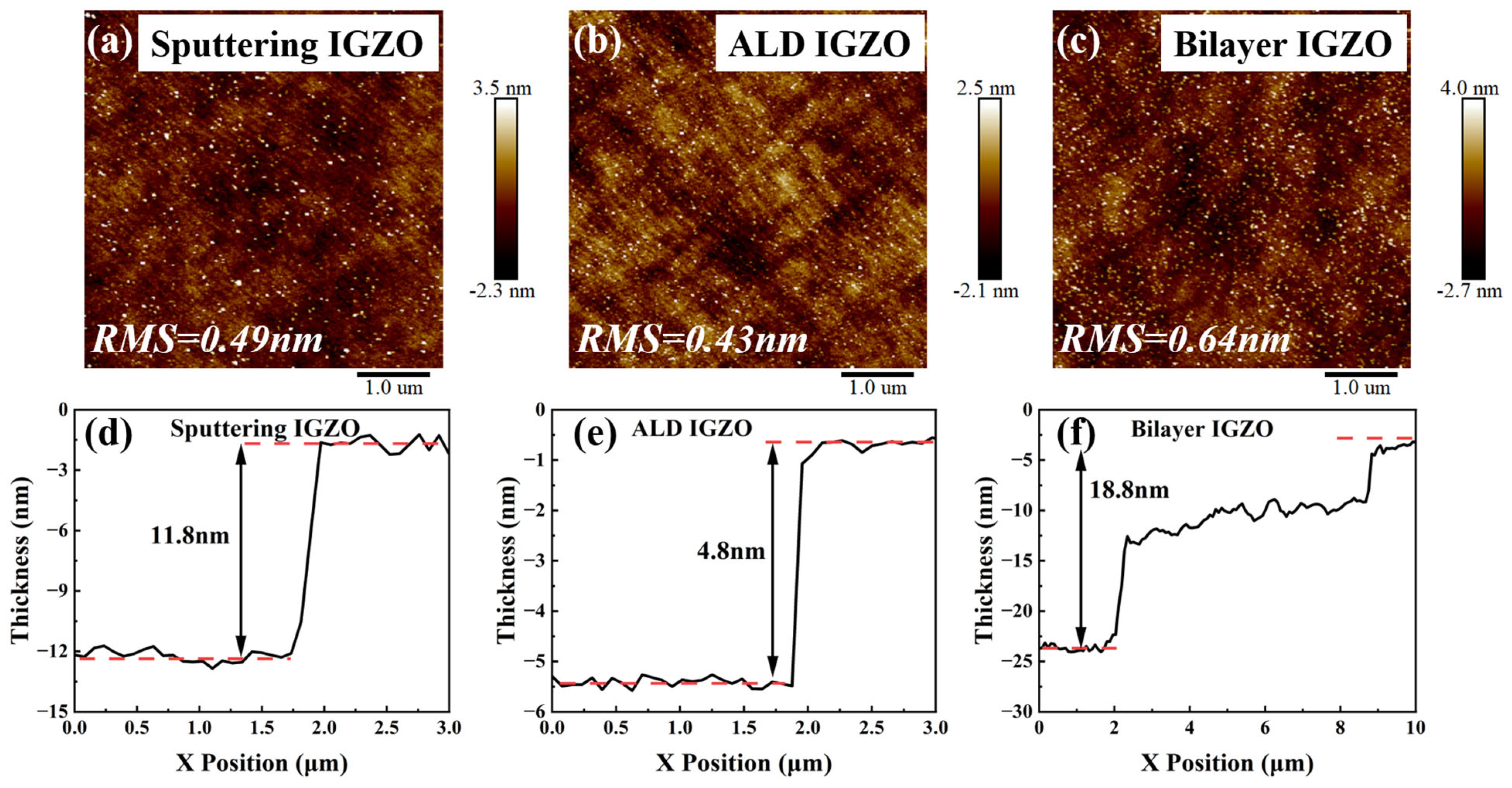
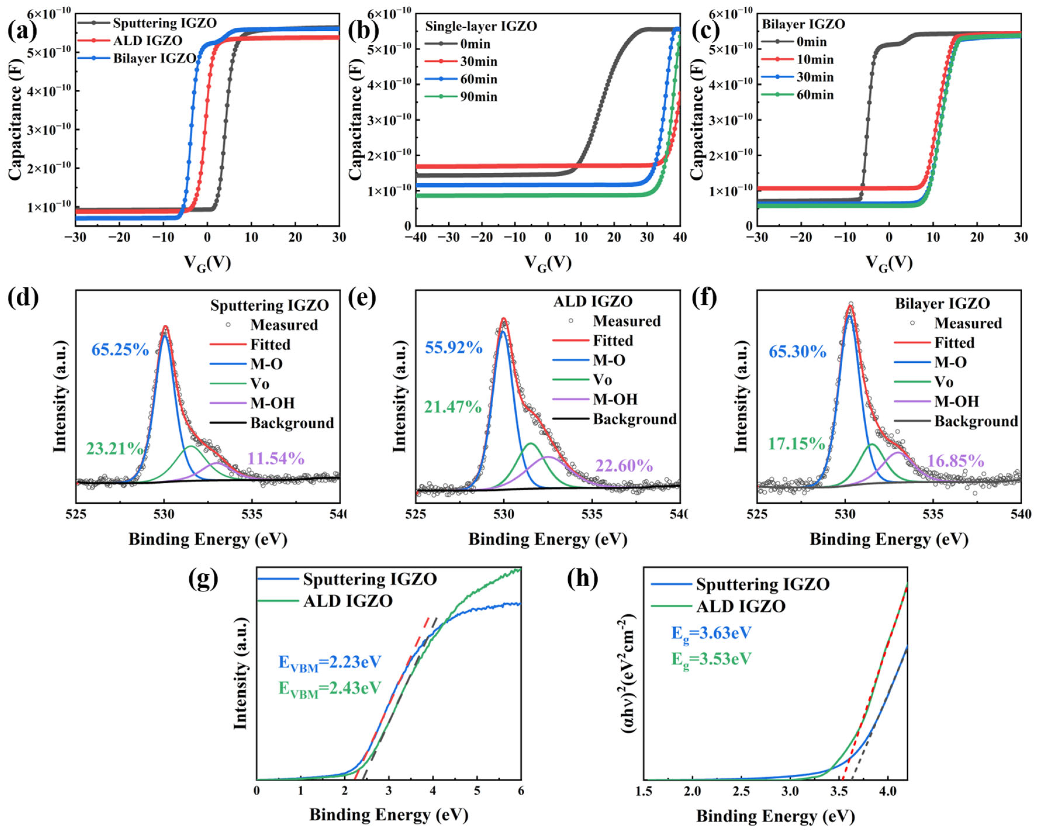
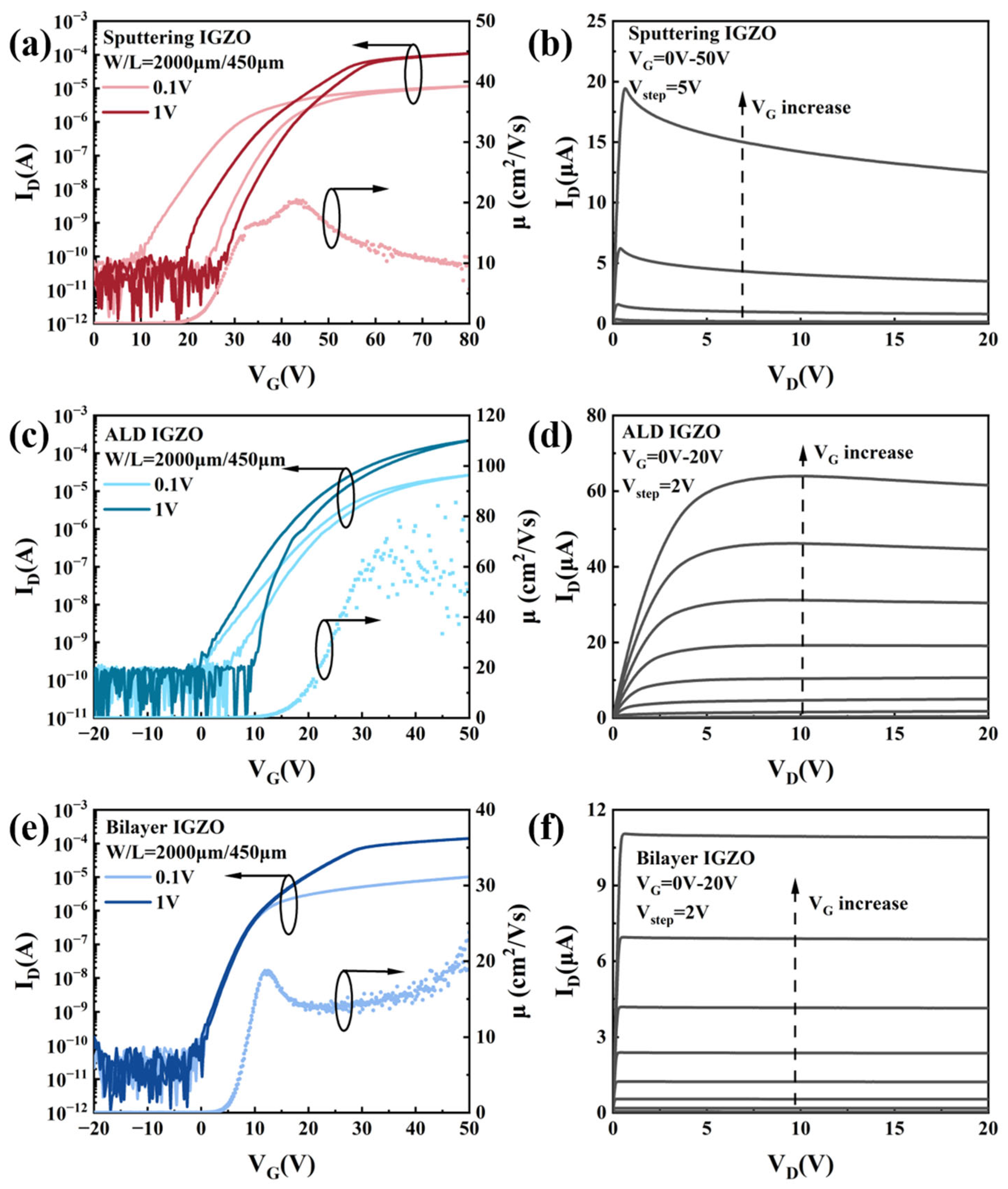
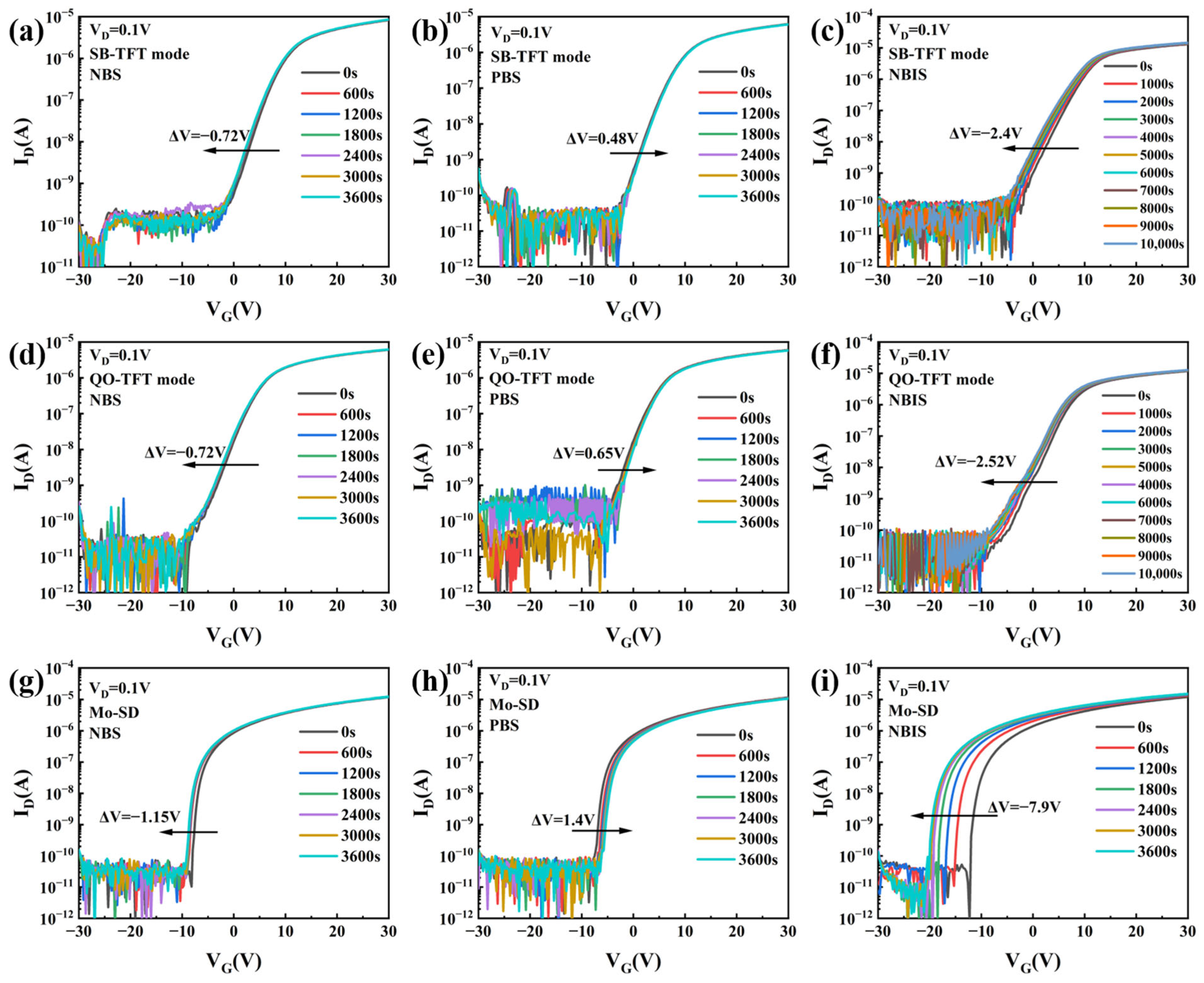
As the substrates, heavily doped p-type Silicon with thermally grown 100 nm SiO2 were sequentially cleaned in acetone and anhydrous ethanol. The IGZO films were deposited using ALD (MNT-D) for 16 cycles on substrates at 250 °C, employing trimethylindium, trimethyl gallium, and diethylzinc as the indium, gallium, and zinc sources (In: Ga: Zn = 10:4:5 at.%). IGZO films were patterned by photolithography (RZJ-390PG-30 photoresists) and wet acid etching in hydrochloric acid for 30 s. Subsequently, Pt electrode was sputtered, followed by a lift-off process. After annealing in air at 350 °C for 2 h, Mo electrode was sputtered to complete the fabrication of the ALD IGZO-based devices. In this work, the fabricated devices have two different channel width-to-length ratios: one is 2000 μm/450 μm, and the other one is 1000 μm/50 to 350 μm. The sputtering IGZO films (In: Ga: Zn = 1:1:1 at.%) were deposited (SYSKEY Technology) for different cycles on the substrates. During the sputtering process, the power is 700 W, and the oxygen argon ratio is 1.5:48.5. Except for annealing in air at 350 °C for 1 h, other processes of sputtering IGZO-based devices are consistent with above. For bilayer IGZO devices, sputtering IGZO films were deposited after patterning the ALD IGZO films and annealing in air at 350 °C for 1 h. The subsequent processes remained identical to the sputtering IGZO-based devices.
The electrical characteristics and stability of the devices were measured at RT using a semiconductor parameter analyzer (B1500A, Agilent Technologies, Santa Clara, CA, USA). The surface roughness of the films was measured using an Atomic Force Microscope (AFM, Bruker Dimension Icon, Cambridge, MA, USA). The oxygen vacancy content and band edge parameters of the IGZO films were analyzed by X-ray Photoelectron Spectroscopy (XPS) and Ultraviolet Photoelectron Spectroscopy (UPS). The transmission spectra of the films deposited on quartz substrates were characterized using a UV spectrophotometer. Capacitance–voltage (CV) curves were examined using the Agilent E4980A.

3. Results

Figure 1a–c illustrates the band diagrams of SB-TFT mode devices. Different work functions between the Pt metal and the IGZO film induce electron flow from the semiconductor to the metal when they contact, forming a high-resistance depletion region. When the Pt electrode serves as the source, electrons need to overcome the Schottky barrier to inject into the semiconductor. The primary mechanisms for electron transport across the Schottky barrier into the semiconductor layer are thermionic emission (TE) and thermionic field emission (TFE). In the linear region, the Schottky barrier is modulated by both drain voltage (VD) and gate voltage (VG). As VD increases, the depletion region gradually shifts toward the interface between the semiconductor and the dielectric layer. In the saturation region, VG modulates the barrier height by adjusting the built-in electric field within the depletion region and controls the saturation current [17,18,19]. The band diagrams of QO-TFT mode devices are shown in Figure 1d–f, and VD will lower the Schottky barrier when the Pt electrode serves as the drain. It is worth noting that all band diagrams have been simulated by TCAD atlas at accurate voltage bias to compare the effect of VD and VG on the Schottky barrier.
Figure 2 shows the surface topography images and the thickness of the fabricated IGZO films. The scan area of each film is 5 μm × 5 μm. The RMS of different IGZO films indicates the smooth surface. The higher RMS of the bilayer film is caused by the ALD IGZO layer, which exhibits higher roughness in comparison to the P-Si/SiO₂ substrates. As shown in Figure 2d–f, the thickness of the sputtering IGZO layer, ALD IGZO layer, and bilayer IGZO are 11.8 nm, 4.7 nm, and 18.8 nm. The C-V curves of different IGZO films with Mo electrode are shown in Figure 3a, and the bilayer film forms the two-dimensional electron gas (2DEG) near VG = 0 V. From the C-V curves in Figure 3b,c, the Schottky contact between Pt electrode and IGZO layer is stable after annealing for 60 min. When the Pt electrode is unannealed, it forms an ohmic contact. As the annealing time increases, a noticeable positive shift is observed. A similar trend was observed in the bilayer, where the 2DEG disappeared, and the curve shows a positive shift as the Pt annealing time increases. This can be explained by the depletion region with low carrier concentration. As the annealing time increases, the barrier height increases until Schottky contact remains stable [20,21]. The XPS measurements are shown in Figure 3d–f. The O1s XPS spectra are deconvoluted into three Gaussian peaks centered at 530.0 ± 0.4 eV, 531.5 ± 0.3 eV, and 532.3 ± 0.4 eV, corresponding to metal–oxygen bonds (M-O), oxygen vacancies (Vo), and specific chemisorbed oxygen impurity bonds (M-OH), respectively. Compared to the single-layer IGZO films, the M-O bonds and M-OH bonds concentration of the bilayer films increase to 65.3% and decrease to 16.85%, respectively. The area of Vo decreases to 17.15%, which is significantly lower than that in the single-layer films. Compared to the sputtering IGZO film, the bilayer film exhibits lower oxygen vacancy, which may be attributed to the discontinuity of the conduction band (formation of 2DEG) and less trapped electrons in the dielectric [22]. The valence band maximum (EVBM) of sputtering IGZO and ALD IGZO films were extracted in Figure 3g, which were 2.23 eV and 2.43 eV. And the obtained Eg of sputtering IGZO and ALD IGZO were 3.63 eV and 3.53 eV, as shown in Figure 3h.
Figure 4 compares the transfer and output characteristic curve of SB-TFT mode devices fabricated with sputtering IGZO, ALD IGZO, and bilayer IGZO, and the channel width-to-length ratio is 2000 μm/450 μm. The transfer curve exhibited a noticeable hysteresis when the sputtering IGZO film was thin, which indicates high defect density in the film and electron trapping when applying VG [23,24]. Compared to conventional TFT with Ohmic contact, the fabricated SBTFTs exhibit degraded subthreshold swing (SS), nearly 2 V/dec in this work, which has been observed in other Schottky barrier devices [11,12,25]. The output curve revealed a lower saturation voltage and a reduced output current. Due to a large number of defects at the channel/dielectric interface and the intrinsic defects in the material, conduction electrons have been trapped by the defects and gradually reduced when applying VD and VG, which corresponds to the large hysteresis and the forward shift in the transfer curves. The increased roughness and concentration of oxygen vacancy in the sputtering IGZO film, as shown in Figure 2a and Figure 3d, also prove that higher density of defects in the film. A similar phenomenon has been observed in the previous results of Schottky barrier transistors [12,26,27,28]. Although the thin sputtering IGZO films can form the Schottky contact with low VDSAT, the thin films with a large number of defects degraded the device performance. In contrast, the ALD IGZO films have better quality, showing a smaller hysteresis and larger current. However, the Schottky contact in the output curve was not obvious. As shown in Figure 4d, the saturation voltage increased slowly with increasing VG. Although ALD films generally exhibit better performance, they are more sensitive to changes at the surface. The Pt electrode was deposited onto the surface of the ALD films via sputtering, and the bombardment caused surface damage easily, leading to the formation of non-uniform Schottky contact. The non-uniform barrier results in part of the conduction current passing through low-barrier regions [11]. To address the above issues of the single-layer IGZO films, we fabricated the SBTFTs with bilayer IGZO films. The bilayer device exhibited nearly negligible hysteresis and a large current in Figure 4e. The calculated linear mobility was between that of the two single-layer films, approximately 20 cm2/V·s. More importantly, the bilayer device demonstrated superior Schottky contact and a flat output current, with a VDSAT of 0.4 V and an output current of about 10 µA at VG = 20 V, which indicates lower output power consumption and higher output resistance. Many studies have explained the improved performance of bilayer structures [29,30,31,32]. The front-channel ALD IGZO film provides a high carrier concentration, which not only provides a larger conduction current but also compensates for the defects of the back-channel layer. Compared to ALD IGZO, the sputtering IGZO film forms a more stable Schottky contact with Pt metal after annealing, thereby serving as the back-channel layer. To facilitate a more intuitive comparative analysis, critical parameters of sputtering IGZO, ALD IGZO, and bilayer IGZO devices are systematically listed in Table 1. As shown in Table 1, the ratio of VDSAT to VG (R = dVDSAT/dVG) is 0.04, 0.6, and 0.036 for devices based on sputtering IGZO, ALD IGZO, and bilayer IGZO. The R value is less than 1 when forming a Schottky contact [33]. A smaller R implies a less effect of the gate voltage on the saturation voltage and a more significant manifestation of the Schottky barrier effect. Meanwhile, the saturation voltage VDSAT ≈ (VG − VTH) × Cox/(Cox + Cs) for SBTFTs, where Cox and Cs are insulator and semiconductor capacitances per unit area [28,34]. For SBTFTs, low saturation voltage means that the value of Cox/(Cox + Cs) should be much less than 1. Utilizing the measured capacitance data, the Cox/(Cox + Cs) value of sputtering, ALD, and bilayer IGZO devices are 0.24, 0.5, and 0.22. The larger calculated Cox/(Cox + Cs) and R of ALD IGZO-based device is considered due to the non-uniform Schottky barrier. Through a comparative analysis of sputtering and ALD IGZO-based devices in the literature, the bilayer IGZO devices fabricated in this article demonstrate superior performance characterized by higher mobility, lower saturation voltage, and enhanced Schottky contact, as evidenced by a smaller R value.
Utilizing the bilayer IGZO devices, we investigated the performance of the dual-mode devices with a channel width of 1000 µm and lengths ranging from 50 to 350 µm. The conduction current of SGT devices is primarily determined by source contact and barrier height rather than the channel because the semiconductor layer under the source would be fully depleted when applying enough VD. Therefore, SGT devices are immune to the change in channel length [11,12,40]. Figure 5a,b show the transfer and output curve of SB-TFT mode devices with different channel lengths. The current exhibited minimal change to the channel length in Figure 5a. The current only increased from 6.68 µA to 9.19 µA as the channel length decreased from 350 µm to 50 µm, and the change in current was significantly smaller than the scale of the channel length. This behavior is attributed to the reverse current of the Schottky barrier, which primarily dominates the conduction current. As shown in Figure 5c,d, although the threshold voltage showed a negative shift due to the lowering of the barrier, the current of the QO-TFT mode device increased from 7.57 µA to 13 µA as the channel length decreased. The VD applied at the barrier acts as a forward bias for the Schottky diode, reducing the barrier and increasing the device’s sensitivity to channel length. In Figure 5d, the device current significantly increases as VD and VG increase. As evidenced by the output curve, the QO-TFT mode device shows the absence of a low VDSAT. In addition, the phenomenon of current blocking was observed at smaller VD and VG, which attenuates as the voltage increases in the inset of Figure 5d. Figure 5e,f extract the current for various channel lengths at VD = 0.1 V, VG = 20 V, and VD = 20 V, VG = 20 V. Notably, the QO-TFT mode devices demonstrate larger output currents and exhibit greater sensitivity to channel length.
Figure 6 illustrates the bias stability test results for SB-TFT mode, QO-TFT mode, and Mo-SD devices. During Negative Bias Stress (NBS) and Positive Bias Stress (PBS), the VG was applied at −20 V and 20 V, respectively. As shown in Figure 6a,b, the threshold voltage shift (ΔV) of the SB-TFT mode under NBS and PBS were −0.72 V and 0.48 V, respectively. In comparison, the ΔV for QO-TFT mode devices were −0.72 V and 0.65 V. The PBS instability can be caused by the electron trapping at the dielectric–channel interface and ambient effect at the back-channel surface. The NBS instability, which is associated with donor states that become positively charged by releasing electrons into the conduction band, remained relatively unchanged during the test. Electrons can be excited and ionized charge-neutral oxygen vacancies (Vo) into positively charged centers (Vo2+) under illumination, thereby injecting free electrons into the conduction band and contributing to a more significantly negative voltage shift [41]. The ΔV were −1.68 V and −1.44 V under NBIS at the bias time t = 3600 s for the SB-TFT mode and QO-TFT mode devices, respectively. Especially, the ΔV was −2.4 V and −2.52 V for the SB-TFT mode and QO-TFT mode devices, respectively, when t = 10,000 s, showing good stability. Figure 6g–i also provide the test results of the Mo-SD device. Table 2 summarizes the ΔV of three devices under stability tests. The observed difference in stability is primarily attributed to the formation of the depletion region [6]. On one hand, the total resistance Rtot = Rc + Rch, where Rch is the channel resistance and Rc is the contact resistance. The low carrier concentration in the depletion region results in the contact resistance being much higher than the channel resistance. Consequently, even though the carrier concentration may vary during the test, which causes a smaller Rc, the total resistance exhibits little change. For the QO-TFT mode structure, as the drain voltage increases, the contact resistance gradually decreases, which causes the change in stability. On the other hand, the electron quasi-Fermi level in the depleted source may be pinned and prevent the accumulation of electrons [42].

4. Conclusions

In this paper, we propose and design high-performance Schottky devices through the bilayer structure. The bilayer devices not only form a good Schottky contact but also exploit the advantages of the front-channel ALD IGZO film, which can repair the defects of the back-channel film and significantly enhance the conduction current of the device. Meanwhile, devices with higher Schottky barriers are less sensitive to channel length. In the comparison of the stability of SB-TFT mode, QO-TFT mode, and Mo-SD devices, we observe the effect of the Schottky barrier response to the various applied VD. Devices with Schottky barriers exhibit better stability than Mo-SD devices. This work offers a strategy to fabricate thinner SBTFTs with excellent performance and deep insights into the behavior of SBTFTs.

Author Contributions

Conceptualization, X.L. and C.L.; methodology, Y.H. and X.L.; validation, Y.H. and X.L.; formal analysis, Y.H., X.L. and C.L.; investigation, Y.H.; resources, C.L.; data curation, Y.H.; writing—original draft preparation, Y.H.; writing—review and editing, M.W., T.W. and C.L.; visualization, Y.H.; supervision, L.Z. and C.L.; project administration, C.L.; funding acquisition, C.L. All authors have read and agreed to the published version of the manuscript.

Funding

This work was supported in part by the National Key Research and Development Program of China under Grant 2022YFB3603901, in part by the National Natural Science Foundation of China under Grant 62004227, and in part by the Science and Technology Projects in Guangzhou under Grant 202201000008.

Data Availability Statement

The data presented in this study are available from the corresponding author upon reasonable request.

Conflicts of Interest

The authors declare no conflicts of interest.

References

  1. Shannon, J.M.; Balon, F. Source-Gated Thin-Film Transistors. Solid State Electron. 2008, 52, 449–454. [Google Scholar] [CrossRef]
  2. Sporea, R.A.; Trainor, M.J.; Young, N.D.; Shannon, J.M.; Silva, S.R.P. Intrinsic Gain in Self-Aligned Polysilicon Source-Gated Transistors. IEEE Trans. Electron Devices 2010, 57, 2434–2439. [Google Scholar] [CrossRef]
  3. Sporea, R.A.; Trainor, M.J.; Young, N.D.; Shannon, J.M.; Silva, S.R.P. Field Plate Optimization in Low-Power High-Gain Source-Gated Transistors. IEEE Trans. Electron Devices 2012, 59, 2180–2186. [Google Scholar] [CrossRef]
  4. Jiang, C.; Choi, H.W.; Cheng, X.; Ma, H.; Hasko, D.; Nathan, A. Printed Subthreshold Organic Transistors Operating at High Gain and Ultralow Power. Science 2019, 363, 719–723. [Google Scholar] [CrossRef]
  5. Kim, Y.; Lee, E.K.; Oh, J.H. Flexible Low-Power Operative Organic Source-Gated Transistors. Adv. Funct. Mater. 2019, 29, 1900650. [Google Scholar] [CrossRef]
  6. Schwarz, M.; Vethaak, T.D.; Derycke, V.; Francheteau, A.; Iniguez, B.; Kataria, S.; Kloes, A.; Lefloch, F.; Lemme, M.; Snyder, J.P.; et al. The Schottky Barrier Transistor in Emerging Electronic Devices. Nanotechnology 2023, 34, 352002. [Google Scholar] [CrossRef]
  7. Xu, X.; Sporea, R.A.; Guo, X. Source-Gated Transistors for Power- and Area-Efficient AMOLED Pixel Circuits. J. Disp. Technol. 2014, 10, 928–933. [Google Scholar] [CrossRef]
  8. Huang, S.; Jin, J.; Kim, J.; Wu, W.; Song, A.; Zhang, J. IGZO Source-Gated Transistor for AMOLED Pixel Circuit. IEEE Trans. Electron Devices 2023, 70, 3637–3642. [Google Scholar] [CrossRef]
  9. Dong, C.; Xu, J.; Zhou, Y.; Zhang, Y.; Xie, H. Light-Illumination Stability of Amorphous InGaZnO Thin Film Transistors in Oxygen and Moisture Ambience. Solid State Electron. 2019, 153, 74–78. [Google Scholar] [CrossRef]
  10. Mativenga, M.; Haque, F.; Billah, M.M.; Um, J.G. Origin of Light Instability in Amorphous IGZO Thin-Film Transistors and Its Suppression. Sci. Rep. 2021, 11, 14618. [Google Scholar] [CrossRef]
  11. Zhang, J.; Wilson, J.; Auton, G.; Wang, Y.; Xu, M.; Xin, Q.; Song, A. Extremely High-Gain Source-Gated Transistors. Proc. Natl. Acad. Sci. USA 2019, 116, 4843–4848. [Google Scholar] [CrossRef] [PubMed]
  12. Li, Y.; Cai, G.; Tang, B.; Zou, S.; Lan, L.; Gong, Z. High-Performance Schottky-Barrier IGZO Thin-Film Transistors Based on Ohmic/Schottky Hybrid Contacts. IEEE Trans. Electron Devices 2024, 71, 6781–6787. [Google Scholar] [CrossRef]
  13. Zhao, Y.; Wang, Z.; Xu, G.; Cai, L.; Han, T.; Zhang, A.; Wu, Q.; Wang, R.; Huang, T.; Cheng, P.; et al. High Performance Indium-Gallium-Zinc Oxide Thin Film Transistor via Interface Engineering. Adv. Funct. Mater. 2020, 30, 2003285. [Google Scholar] [CrossRef]
  14. Samanta, S.; Chand, U.; Xu, S.; Han, K.; Wu, Y.; Wang, C.; Kumar, A.; Velluri, H.; Li, Y.; Fong, X.; et al. Low Subthreshold Swing and High Mobility Amorphous Indium–Gallium–Zinc-Oxide Thin-Film Transistor with Thin HfO2 Gate Dielectric and Excellent Uniformity. IEEE Electron Device Lett. 2020, 41, 856–859. [Google Scholar] [CrossRef]
  15. Cho, M.H.; Seol, H.; Yang, H.; Yun, P.S.; Bae, J.U.; Park, K.-S.; Jeong, J.K. High-Performance Amorphous Indium Gallium Zinc Oxide Thin-Film Transistors Fabricated by Atomic Layer Deposition. IEEE Electron Device Lett. 2018, 39, 688–691. [Google Scholar] [CrossRef]
  16. Kim, M.J.; Park, H.J.; Yoo, S.; Cho, M.H.; Jeong, J.K. Effect of Channel Thickness on Performance of Ultra-Thin Body IGZO Field-Effect Transistors. IEEE Trans. Electron Devices 2022, 69, 2409–2416. [Google Scholar] [CrossRef]
  17. Valletta, A.; Mariucci, L.; Rapisarda, M.; Fortunato, G. Principle of Operation and Modeling of Source-Gated Transistors. J. Appl. Phys. 2013, 114, 064501. [Google Scholar] [CrossRef]
  18. Shannon, J.M.; Gerstner, E.G. Source-Gated Thin-Film Transistors. IEEE Electron Device Lett. 2003, 24, 405–407. [Google Scholar] [CrossRef]
  19. Shannon, J.M.; Sporea, R.A.; Georgakopoulos, S.; Shkunov, M.; Silva, S.R.P. Low-Field Behavior of Source-Gated Transistors. IEEE Trans. Electron Devices 2013, 60, 2444–2449. [Google Scholar] [CrossRef]
  20. Lü, Y.-J.; Lin, Z.-J.; Zhang, Y.; Meng, L.-G.; Cao, Z.-F.; Luan, C.-B.; Chen, H.; Wang, Z.-G. Influence of Thermal Stress on the Characteristic Parameters of AlGaN/GaN Heterostructure Schottky Contacts. Chin. Phys. B 2011, 20, 047105. [Google Scholar] [CrossRef]
  21. Zhao, J.; Lin, Z.; Lu, Y.; Corrigan, T.D.; Meng, L.; Zhang, Y.; Wang, Z.; Chen, H. Influence of Ni Schottky Contact Thickness on Two-Dimensional Electron-Gas Sheet Carrier Concentration of Strained Al0.3Ga0.7N/GaN Heterostructures. J. Semicond. 2010, 31, 084007. [Google Scholar] [CrossRef]
  22. Bae, S.-H.; Moon, S.-H.; Kwon, Y.H.; Nak-Jin-Seong; Choi, K.-J.; Yoon, S.-M. Synergic Strategies of Composition-Modified Bilayer Channel Configuration and Ozone-Processed Gate Stacks for Atomic-Layer Deposited In-Ga-Zn-O Thin-Film Transistors. J. Alloys Compd. 2022, 906, 164283. [Google Scholar] [CrossRef]
  23. Lee, S.Y.; Kim, D.H.; Chong, E.; Jeon, Y.W.; Kim, D.H. Effect of Channel Thickness on Density of States in Amorphous InGaZnO Thin Film Transistor. Appl. Phys. Lett. 2011, 98, 122105. [Google Scholar] [CrossRef]
  24. Hsu, C.-C.; Chen, H.-P.; Ting, W.-C. Correlation between Carrier Concentration Distribution, I-V and C-V Characteristics of a-InGaZnO TFTs. J. Disp. Technol. 2015, 12, 328–337. [Google Scholar] [CrossRef]
  25. Ko, R.-M.; Wang, S.-J.; Huang, S.-J.; Wu, C.-H.; Chen, W.-H.; Cheng, H.-C. Enhancing Photodetection Performance of UV Photodetectors with Stacked Pt/NiO Dual Capping Layers on IGZO Thin-Film Transistors. AIP Adv. 2023, 13, 075307. [Google Scholar] [CrossRef]
  26. Zhuang, X.; Kim, J.-S.; Huang, W.; Chen, Y.; Wang, G.; Chen, J.; Yao, Y.; Wang, Z.; Liu, F.; Yu, J.; et al. High-Performance and Low-Power Source-Gated Transistors Enabled by a Solution-Processed Metal Oxide Homojunction. Proc. Natl. Acad. Sci. USA 2023, 120, e2216672120. [Google Scholar] [CrossRef]
  27. Bestelink, E.; Zschieschang, U.; Askew, L.; Klauk, H.; Sporea, R.A. Organic Source-Gated Phototransistors with > 104 Photo-To-Dark Current Ratio in the Visible Range at Zero Gate-Source Bias. Adv. Opt. Mater. 2024, 12, 2301931. [Google Scholar] [CrossRef]
  28. Bestelink, E.; Zschieschang, U.; Bandara, R.M.I.; Klauk, H.; Sporea, R.A. The Secret Ingredient for Exceptional Contact-Controlled Transistors. Adv. Electron. Mater. 2022, 8, 2101101. [Google Scholar] [CrossRef]
  29. Zhu, Q.; Huang, Y.; Wu, J.; Guo, M.; Ou, H.; Liu, B.; Lu, X.; Chen, J.; Liang, X.; Wu, Q.; et al. Enhanced Performance and Stability of Atomic Layer Deposited In₂O₃ Transistors With Multi-Function Cation-Doped ZnSnO Layers. IEEE Electron Device Lett. 2024, 45, 845–848. [Google Scholar] [CrossRef]
  30. Park, J.C.; Lee, H.-N. Improvement of the Performance and Stability of Oxide Semiconductor Thin-Film Transistors Using Double-Stacked Active Layers. IEEE Electron Device Lett. 2012, 33, 818–820. [Google Scholar] [CrossRef]
  31. Hong, S.; Park, J.W.; Kim, H.J.; Kim, Y.; Kim, H.J. A Review of Multi-Stacked Active-Layer Structures for Solution-Processed Oxide Semiconductor Thin-Film Transistors. J. Inf. Disp. 2016, 17, 93–101. [Google Scholar] [CrossRef]
  32. Guo, M.; Ou, H.; Xie, D.; Zhu, Q.; Wang, M.; Liang, L.; Liu, F.; Ning, C.; Cao, H.; Yuan, G.; et al. Critical Assessment of the High Carrier Mobility of Bilayer In2O3/IGZO Transistors and the Underlying Mechanisms. Adv. Electron. Mater. 2023, 9, 2201184. [Google Scholar] [CrossRef]
  33. Raj, R.B.; Tripathi, A.K.; Mahato, P.K.; Nair, S.; Deepak; Shahana, T.K.; Mukundan, T. Effect of Active Layer Thickness Variation on Scaling Response in A-IGZO Thin Film Transistors under Schottky Limited Operation. Semicond. Sci. Technol. 2021, 36, 115007. [Google Scholar] [CrossRef]
  34. Li, Y.; Zhou, Y.; Zou, S.; Lan, L.; Gong, Z. Insight into the Evolution of Electrical Properties for Schottky-Barrier IGZO Thin-Film Transistors with Cu-Based Schottky Contacts. Appl. Phys. Lett. 2023, 123, 103503. [Google Scholar] [CrossRef]
  35. Sporea, R.A.; Niang, K.M.; Flewitt, A.J.; Silva, S.R.P. Novel Tunnel-Contact-Controlled IGZO Thin-Film Transistors with High Tolerance to Geometrical Variability. Adv. Mater. 2019, 31, 1902551. [Google Scholar] [CrossRef]
  36. Tu, Y.-F.; Huang, J.-W.; Chang, T.-C.; Hung, Y.-H.; Tai, M.-C.; Chen, J.-J.; Lin, S.-K.; Zhou, K.-J.; Chien, Y.-T.; Huang, H.-C.; et al. Stably Saturated Output Current Characteristics and Hot-Carrier Reliability of a-InGaZnO Thin-Film Transistors With Source-Connected Field Plate. IEEE Trans. Electron Devices 2023, 70, 4669–4673. [Google Scholar] [CrossRef]
  37. Bestelink, E.; Niang, K.M.; Wyatt-Moon, G.; Flewitt, A.J.; Sporea, R.A. Promoting Low-Voltage Saturation in High-Performance a-InGaZnO Source-Gated Transistors. IEEE Trans. Electron Devices 2024, 71, 581–587. [Google Scholar] [CrossRef]
  38. Lee, D.-H.; Kwon, Y.-H.; Seong, N.-J.; Choi, K.-J.; Kim, G.; Yoon, S.-M. Analysis on Contact Resistance and Effective Channel Length of Thin Film Transistors Using Composition-Modified In–Ga–Zn-O Active Channels Prepared with Atomic Layer Deposition and Various Electrode Materials. ACS Appl. Electron. Mater. 2022, 4, 6215–6228. [Google Scholar] [CrossRef]
  39. Chen, Q.; Wang, L.; Duan, X.; Guo, J.; Wang, Z.; Huang, K.; Feng, J.; Sun, Y.; Jiao, G.; Jing, W.; et al. Investigation of Asymmetric Characteristics of Novel Vertical Channel-All-Around (CAA) In-Ga-Zn-O Field Effect Transistors. IEEE Electron Device Lett. 2022, 43, 894–897. [Google Scholar] [CrossRef]
  40. Wang, G.; Zhuang, X.; Huang, W.; Yu, J.; Zhang, H.; Facchetti, A.; Marks, T.J. New Opportunities for High-Performance Source-Gated Transistors Using Unconventional Materials. Adv. Sci. 2021, 8, 2101473. [Google Scholar] [CrossRef]
  41. Conley, J.F. Instabilities in Amorphous Oxide Semiconductor Thin-Film Transistors. Ieee Trans. Device Mater. Reliab. 2010, 10, 460–475. [Google Scholar] [CrossRef]
  42. Shannon, J.M. Stable Transistors in Hydrogenated Amorphous Silicon. Appl. Phys. Lett. 2004, 85, 326–328. [Google Scholar] [CrossRef]
Figure 1. Band diagrams of SB-TFT mode devices (a) at zero VD and zero VG, (b) at VD = 0.1 V only, and (c) at VD = 0.1 V, VG = 5 V. Band diagrams of QO-TFT mode devices (d) at zero VD and zero VG, (e) at VD = 0.1 V only, and (f) at VD = 0.1 V, VG = 5 V. (g,h) Structure of Schottky contact device and Ohmic contact device.
Electronics 14 01380 g001
Figure 2. (ac) AFM topography images of sputtering IGZO, ALD IGZO, and bilayer films. (df) Thickness measurement of corresponding IGZO films.
Electronics 14 01380 g002
Figure 3. (a) C-V curves of the MIS structure of different IGZO films with Mo electrode. (b,c) C-V curves of Pt electrode on single-layer and bilayer IGZO films for different annealing times. (df) XPS spectra of O1s for sputtering IGZO, ALD IGZO, and bilayer IGZO films. (g,h) XPS valence spectra and optical band-gap spectra for sputtering and ALD IGZO films.
Electronics 14 01380 g003
Figure 4. Transfer and output characteristic curve of SB-TFT mode devices with (a,b) sputtering IGZO, (c,d) ALD IGZO, and (e,f) bilayer IGZO.
Electronics 14 01380 g004
Figure 5. Transfer and output characteristic curves of (a,b) SB-TFT mode devices and (c,d) QO-TFT mode devices with different channel lengths. (e,f) Current as a function of channel length extracted at VD = 0.1 V, VG = 20 V and VD = 20 V, VG = 20 V.
Electronics 14 01380 g005
Figure 6. Transfer characteristic curves of (ac) SB-TFT mode, (df) QO-TFT mode, and (gi) Mo-SD devices at different stress times (0–3600 s, with a time step of 600 s) under NBS, PBS, and NBIS tests.
Electronics 14 01380 g006
Table 1. Performance comparison of sputtering IGZO, ALD IGZO, and bilayer IGZO devices.
Channelμ (cm2/Vs)IDSAT (μA)VDSAT (V)dVDSAT/dVGReference
Sputtering IGZO1013 @VG = 50 V0.65 @VG = 50 V~0.04This work
ALD IGZO4560 @VG = 20 V7.5 @VG = 20 V~0.6This work
Bilayer IGZO2011 @VG = 20 V0.4 @VG = 20 V~0.036This work
Sputtering IGZO-34 @VG = 40 V<3 @VG = 40 V~0.1[11]
Sputtering IGZO-0.7 @VG = −8.4 V3 @VG = −8.4 V0.12[35]
Sputtering IGZO-2.7 @VG = 10 V3 @VG = 10 V~0.4[36]
Sputtering IGZO4.511 @VG = 20 V2.7 @VG = 20 V0.12[37]
ALD IGZO2.85.4 @VG = 10 V--[38]
ALD IGZO-23 @VG = 1 V0.6 @VG = 1 V-[39]
Table 2. Comparison of ΔV under NBS, PBS, and NBIS tests.
Mo-SDSB-TFT ModeQO-TFT Mode
VD(V)0.10.10.1
ΔVNBS (V)−1.15−0.72−0.72
ΔVPBS (V)1.40.650.48
ΔVNBIS (V)−7.9−1.44−1.68
Disclaimer/Publisher’s Note: The statements, opinions and data contained in all publications are solely those of the individual author(s) and contributor(s) and not of MDPI and/or the editor(s). MDPI and/or the editor(s) disclaim responsibility for any injury to people or property resulting from any ideas, methods, instructions or products referred to in the content.

