Article

Investigation of the Effect of Gate Oxide Screening with Adjustment Pulse on Commercial SiC Power MOSFETs

by
Michael Jin
1,*,
Monikuntala Bhattacharya
1,
Hengyu Yu
1,
Jiashu Qian
1,
Shiva Houshmand
1,
Atsushi Shimbori
2,
Marvin H. White
1 and
Anant K. Agarwal
1
1
Department of Electrical and Computer Engineering, The Ohio State University, Columbus, OH 43210, USA
2
Ford Motor Company, Dearborn, MI 48124, USA
*
Author to whom correspondence should be addressed.
Electronics 2025, 14(7), 1366; https://doi.org/10.3390/electronics14071366
Submission received: 26 February 2025 / Revised: 21 March 2025 / Accepted: 27 March 2025 / Published: 28 March 2025

Abstract

:
This paper presents a method to recover the negative threshold voltage shift during high field gate oxide screening of 1.2 kV 4H-SiC MOSFETs with an additional adjustment gate voltage pulse. To reduce field failure rates of the MOSFETs in operation, manufacturers perform a screening treatment to remove devices with extrinsic defects in the oxide. Current gate oxide screening procedures are limited to oxide fields at or below ~9 MV/cm for short durations (<1 s), which is not enough to remove all the devices with extrinsic defects. The results show that by implementing a lower field gate pulse, the threshold voltage shift can be partially recovered, and therefore the maximum screening field and time can be increased. However, both the initial screening pulse and the adjustment pulse require careful calibration to prevent significant degradation of the device threshold voltage, on-resistance, interface state density, or intrinsic lifetime. With a well calibrated set of pulses, higher screening fields can be utilized without significantly damaging the devices. This leads to an improvement in the overall screening efficiency of the process, reducing the number of devices with extrinsic oxide defects entering the field, and improving the reliability of the SiC MOSFETs in operation.

1. Introduction

Silicon carbide (SiC) is a wide-bandgap material gaining widespread traction in industrial and power applications due to its high critical electric field, thermal conductivity, and saturation velocity [1]. In particular, many manufacturers in the electric vehicle (EV) industry are turning to 4H-SiC power MOSFETs to replace current Si IGBTs in order to reap benefits such as lower on-state resistance and reduced switching losses [2,3]. Due to the stringent safety requirements for these applications, the reliability of the SiC MOSFETs is paramount. One major area of concern for the SiC MOSFET is the gate oxide reliability, particularly the high rate of early oxide failures in the field due to the high density of extrinsic defects [4,5,6,7,8].
These extrinsic defects can be due to contamination in the oxide, defects at the SiC/SiO2 interface, and/or defects within the oxide itself, such as pits, voids, porous oxide, etc., as shown in Figure 1a [6,8,9]. This is defined by the oxide thinning model, where defects in the oxide are treated as local points of thin oxide. Therefore, at a given gate voltage, the gate oxide around these defects experiences a locally high oxide electric field (Eox) which causes the devices to break down sooner compared to an oxide without defects, seen in the Weibull plot extrinsic tail in Figure 1b [7,9,10]. This means that there is a screening voltage that is above the breakdown voltage of some oxide defects but below the breakdown voltage of the bulk oxide. By increasing the screening voltage, it is possible to break down more devices with defects with the added risk of device characteristic shift or reduced intrinsic lifetime for non-defected devices. However, most device manufacturers do not follow a sufficiently aggressive screening regime to fully filter out devices with extrinsic defects, causing early failures in the field.
The efficiency of a screening process can be defined as
η = V s c r e e n V u s e
where η is the screening efficiency, Vscreen is the screening voltage, and Vuse is the operational gate voltage, usually around 20 V [6,12]. In other words, the higher the ratio between the screening voltage and operational voltage, the more efficient the process will be at removing devices with extrinsic gate oxide defects.
Generally, a gate oxide screening process applies a high gate voltage pulse with the goal of removing devices with extrinsic defects while maintaining intrinsic lifetime and electrical characteristics of healthy devices [13]. Recent approaches have led to the introduction of higher field screening (Eox < 9 MV/cm) [14] for short durations. The screening field and duration are limited by the downwards threshold voltage (Vth) shift at higher oxide electric fields. The main cause for this threshold voltage shifting is the hole injection and charge trapping in the oxide at high oxide electric fields. At such fields, holes are generated in the polysilicon due to impact ionization and then are trapped in the oxide [14,15,16]. This causes the net charge in the oxide to increase positively, decreasing the Vth. In this case, the screening efficiency of the technique is limited by the threshold voltage shift, which is dictated by the charge trapping in the oxide. The efficiency can be further improved by increasing either the screening time, temperature, or voltage; however, care must be taken to make sure that the healthy device characteristics and intrinsic lifetimes do not significantly degrade.
In order to improve screening efficiency while maintaining current device electrical characteristics, the screening with adjustment pulse (SWAP) technique is investigated [11]. This room-temperature method applies an extremely high gate voltage pulse (corresponding to Eox ≥ 9 MV/cm) for a longer period of time (≥1 s), which purposefully shifts the threshold voltage down. A lower field pulse is then applied to recover the threshold voltage shifts. This adjustment pulse can also be thought of as an additional low-field screening pulse. In the proposed SWAP method, the screening efficiency is improved as a higher screening voltage can be applied without degrading the device’s electrical characteristics, reducing the field failure rate of the screened devices. The screening procedure is performed at room temperature in order to facilitate the high throughput of devices through the process. Industrial manufacturers may need to screen thousands of devices for gate oxide defects before the MOSFETs can enter into application use. By performing SWAP at room temperature, the need for a high temperature screening setup is negated, and the total turnaround time is reduced, lowering costs. Additionally, the screening efficiency mainly depends on the screening voltage, and temperature plays a much smaller role [6]. Therefore, it is beneficial to trade off the high screening temperature for higher screening voltage as is undertaken in SWAP.
In this work, the effects of the SWAP screening technique are investigated on commercial 1.2 kV 4H-SiC MOSFETs with planar and trench gate structures. The effects of SWAP on the device Vth, on-resistance (Rds-on), and density of interface traps (Dit) are presented and discussed. Finally, constant-voltage time-dependent dielectric breakdown (CV-TDDB) measurements are performed to monitor the device’s intrinsic lifetime. By screening at higher gate voltages and durations, the SWAP technique aims to improve the industry screening efficiency, reducing field failure rates, and enhancing the reliability of the SiC MOSFETs in operation.

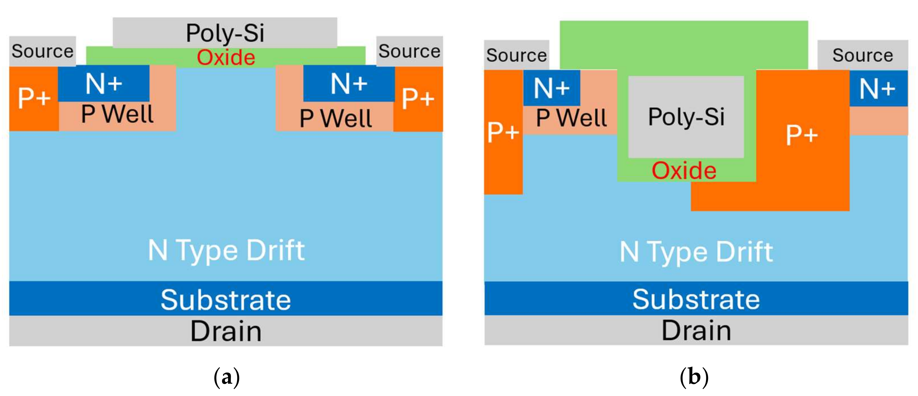
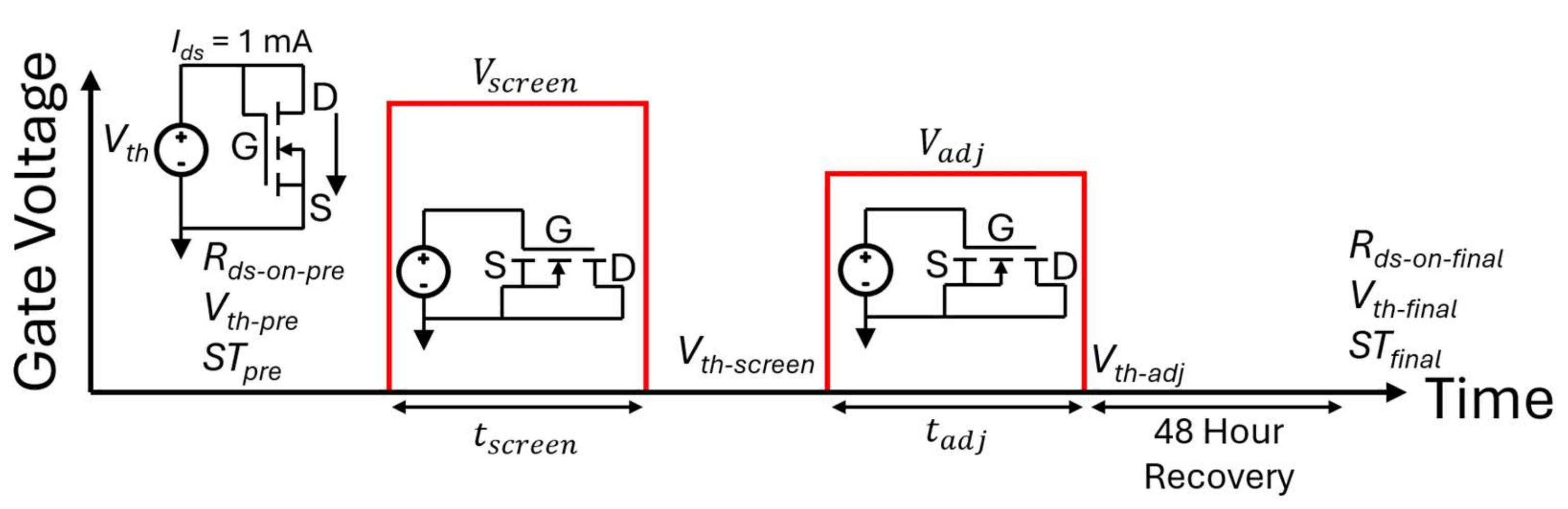
2. Materials and Methods

The details of the 1.2 kV commercial SiC MOSFETs from Vendors F, D, and B used in this work are shown in Table 1. The devices from Vendor F and Vendor D are both planar, while the devices from Vendor B are asymmetric trench devices. A schematic for the planar and asymmetric trench MOSFETs are shown in Figure 2a,b, respectively. Prior to screening, the oxide thickness (tox) of each vendor is estimated by performing a gate ramp-to-breakdown measurement at 150 °C. A sample of devices from each vendor has the drain and source shorted to ground, while the gate is ramped until the oxide breaks down. An average breakdown voltage is taken, and then divided by the critical electric field of SiO2 (taken to be ~11 MV/cm [5]) to estimate the tox for each vendor.
All measurements and procedures were performed at room temperature on a Keysight B1506A parametric analyzer. The threshold voltages were measured by the constant current method, as defined in the vendor datasheet, where the gate and drain are tied and ramped together until a target drain current of 1 mA is measured. Additionally, the Rds-on for each device was measured with 20 V on the gate at the rated drain current. Sub-threshold measurements were also performed in order to estimate the device Dit by measuring the drain current of the transfer characteristics at subthreshold region while holding the drain voltage at 100 mV [17].
To calculate the Dit, we first have to understand the subthreshold drain current equation given as
I d s = I 0 e q V g s n k T 1 e q V d s k T
where I0 is the drain current with no gate voltage, T (K) is the temperature, k is the Boltzmann constant (eV/K), and n is the ideality factor [17]. n is given by
n = 1 + C D + C i t C o x
where Cd is the depletion capacitance, Cit is the interface trap capacitance per unit area, and Cox is the oxide capacitance calculated by dividing the permittivity of SiO2 by the estimated thickness of the oxide [17]. From the Cit, the Dit with respect to the surface potential ϕs can be calculated as
D i t ϕ s = C i t q .
To obtain Dit with respect to the trap level, we have to calculate the energy difference of the conduction band at the interface (EC) and the trap energy level (ET) as a function of surface potential defined as
E C E T = E g 2 q ϕ F 2.3 k T q log I d s 2 ϕ F I d s ϕ s
where Eg is the bandgap of SiC (~3.26 eV), and ϕF is the Fermi level [17]. With Equations (4) and (5), the energy dependent Dit profile with respect to the trap level position compared to the conduction band edge at the surface can be plotted, allowing us to see how the interface trap density changes as we apply the screening conditions [17].
Figure 3 shows the step-by-step testing procedure of the SWAP methodology. First, prescreen threshold voltage (Vth-pre), on-resistance (Rds-on-pre), and sub-threshold (STpre) measurements are conducted. Then, the initial oxide screening pulse with voltage Vscreen for duration tscreen is applied and the gate leakage current is monitored. An intermediate threshold voltage Vth-screen is measured before the adjustment pulse with voltage Vadj for duration tadj is applied. Then, a post-adjustment threshold voltage Vth-adj is measured before a 48 h recovery period. Both the initial screening pulse and the adjustment pulse voltage magnitudes are set by multiplying a desired oxide field (Escreen and Eadj respectively) by the estimated device oxide thickness. Finally, post-recovery threshold voltage (Vth-final), on-resistance (Rds-on-final), and sub-threshold (STfinal) are measured.
In order to normalize the screening conditions to account for different oxide thicknesses, most of the analysis is performed with regard to the applied oxide field rather than an absolute voltage. To quantify the shift in electrical characteristics, the change in device parameters is defined as the difference between the post-recovery values and the pre-screen values. In other words, the Vth shift for a given device is defined as
V t h = V t h f i n a l V t h p r e
and the Rds-on shift is defined as
R d s o n = R d s o n p r e R d s o n f i n a l .
Since there are variations in the Vth that are intrinsic to the devices (as shown in Figure 4 for Vendors F, D, and B used in this work), rather than using just the total shift in voltage, a percentage shift relative to the original pre-screen threshold voltage for each device is calculated. To normalize the amount shifted to the original values, the percent ∆Vth is given by
V t h % = V t h V t h p r e × 100 %
and the percent ΔRds-on by
R d s o n % = R d s o n R d s o n p r e × 100 % .
To ensure that device characteristics are not shifting dramatically due to the screening process, the targeted percent shift in the Vth and Rds-on is ±5%. The high voltage screening can potentially introduce new traps in the interface, so it is essential to look into the Dit profile at ECET ~0.1 eV. To check the intrinsic lifetime of the devices after screening, CV-TDDB measurements are conducted at 150 °C for both screened and unscreened devices, and the resulting Weibull plots are compared. For this measurement, 10 devices per screening condition are placed in parallel in a high temperature chamber with their drains and sources shorted to ground, while a constant high voltage stress is applied to the gates [5]. Time-to-failure is measured for each device, and a Weibull plot is generated for each screening condition. If the intrinsic lifetime is minimally affected by the SWAP procedure, then the Weibull plots from the unscreened and screened devices should be very close to each other.

3. Results

This section discusses the SWAP calibration process and covers the results of the SWAP experiments on the DUTs from Vendors F, D, and B. In order to calibrate the SWAP screening process, first a ∆Vth with respect to screening time and field with no adjustment pulse is measured. Then, an appropriate screening field and time are chosen where a significant negative shift in the threshold voltage is seen. Then, an appropriate adjustment pulse field and duration are calibrated through trial and error until the ∆Vth is brough back within acceptable values. Once both the screening and adjustment pulse have been calibrated, then a larger sample can be screened at those conditions. At this point, the ΔRds-on, Dit, and change in intrinsic lifetime can be measured. If all are within acceptable limits, then the calibrated pulses can be applied for any device from that specific device design or part number. This process is shown in the following subsection.

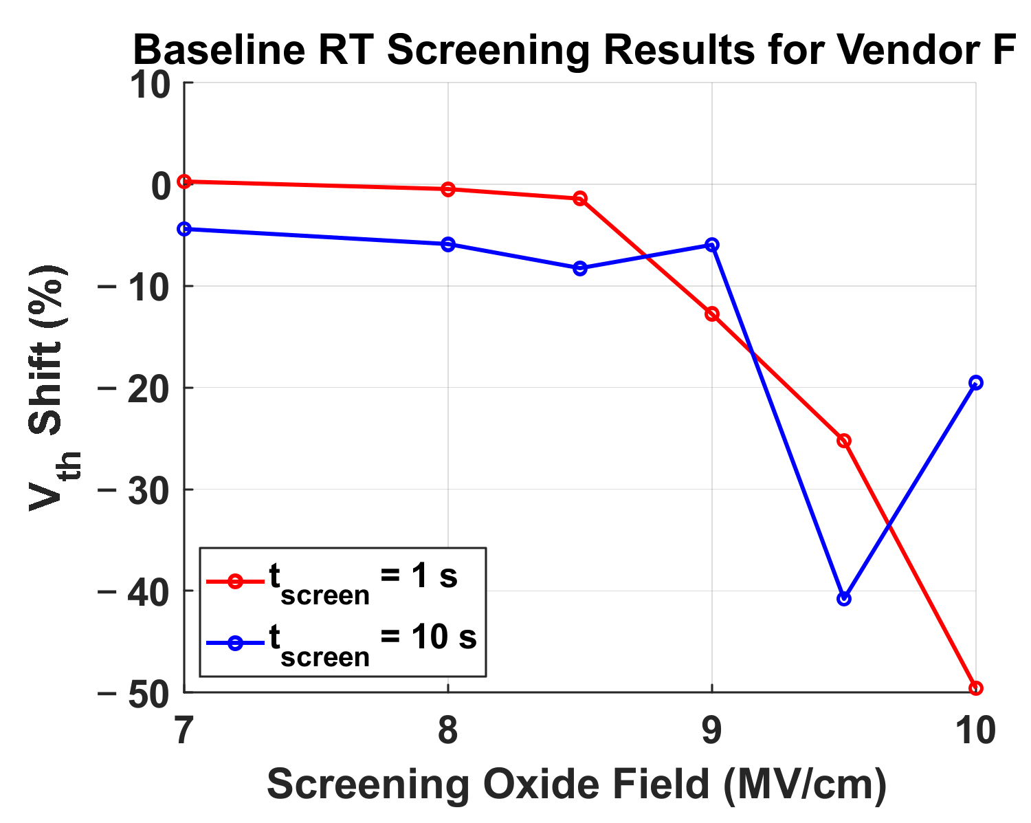
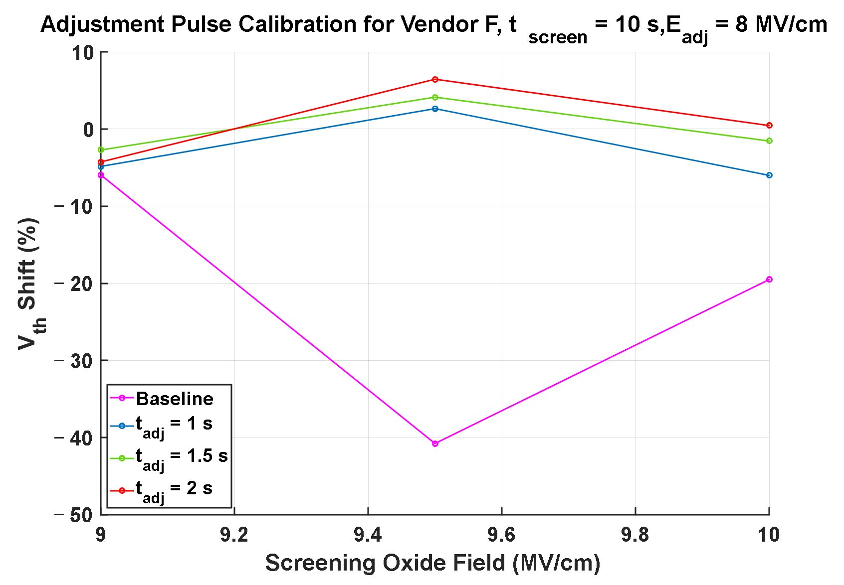
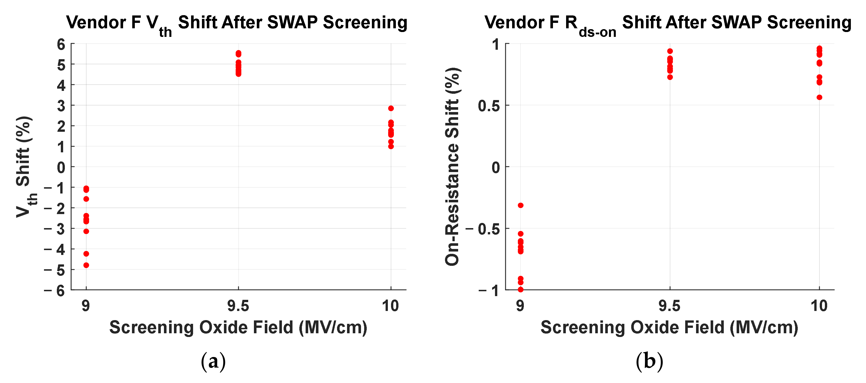
3.1. Calibration and Results for Vendor F1

The first step to calibrate the SWAP procedure is to see how the threshold voltage shifts without any adjustment pulse post-screening as a baseline measurement. To do this, each device is screened at room temperature at a single Escreen ranging from 7.5 MV/cm to 10 MV/cm with a 0.5 MV/cm step for a single tscreen from 1 s to 10 s, with Vth measurements performed before and after the screen, and after a 48 h recovery period. The baseline screening results from Vendor F are shown in Figure 5, where each datapoint is an individual DUT. The effects of hole trapping can be clearly seen as the Vth drops off steeply at around Escreen of 9 MV/cm. Additionally, as tscreen increases from 1 s to 10 s, it is apparent that hole trapping is dominant even at fields as low as 7 MV/cm due to the higher negative magnitude of ∆Vth. In order to maximize the screening efficiency, the SWAP tscreen was held at 10 s and the Escreen was set at 9 MV/cm, 9.5 MV/cm, and 10 MV/cm. Then, the adjustment pulse was calibrated. In this case, an Eadj of 8 MV/cm was chosen based on the baseline measurements to prevent hole trapping, and tadj of 1 s, 1.5 s, and 2 s were tested, with the ΔVth measurements shown in Figure 6. By comparing the ∆Vth of the devices that were exposed to the adjustment pulse to the baseline measurements, it can be seen that the adjustment pulse can effectively reduce the magnitude of the ∆Vth to acceptable levels. Based on these results, the tadj for this vendor was set to 2 s. Table 2 summarizes the final SWAP conditions for the devices from Vendor F.
Once the SWAP conditions had been set from the calibration measurements, a set of 10 devices was screened under each condition to fully understand its effects on the Vth, Rds-on, Dit, and intrinsic lifetime. Figure 7a,b shows the distribution of ΔVth and ΔRds-on for each screening condition, respectively. It can be seen that the distribution for the ΔVth is roughly within the acceptable ±5% range for all SWAP conditions, and notably all of the ΔRds-on is tightly within ±1%. The changes in Rds-on are most likely due to the changes in the Vth rather than changes in the actual resistance, as the ΔRds-on mirrors the ΔVth for each screening condition. There are two main points to draw from this. One is that we are able to massively increase the screening efficiency by increasing the Escreen and tscreen. The second point is that we can prevent the dramatic decrease in the Vth due to hole trapping in the oxide from the high initial Escreen by applying a follow-up adjustment pulse without effecting the Rds-on significantly.
Figure 8 presents the Weibull plots and fit lines comparing the lifetimes of the screened DUTs from each condition to those of a set of unscreened devices at 150 °C and at a gate oxide electric field of 8.9 MV/cm or roughly 34 V. The sample size for each condition was 10 devices. It can be seen that the fitted intrinsic lifetimes of the screened DUTs are actually longer than those of the unscreened DUTs. This is due to the device-to-device variation and natural variability in oxide lifetime under the same stress conditions and is not a concern. What should be noted, however, is that the intrinsic lifetime of all devices, screened or unscreened, is roughly the same. Therefore, for the three set SWAP conditions for Vendor F, none of them reduced the intrinsic lifetime of the DUTs.
Figure 9a–c shows a representative sample of the energy-dependent Dit distribution before and after the SWAP procedure for the three screening conditions (9 MV/cm, 9.5 MV/cm, and 10 MV/cm, respectively) for Vendor F from ECET of 0.1 eV to 0.4 eV. It can be seen that as the Escreen increases, so does the Dit close to the conduction band edge. However, as seen from Figure 7, this increase in Dit due to the SWAP process does not significantly affect the device Rds-on or the device Vth. Therefore, this Dit increase is negligible in the application use of the DUT after screening and does not negatively affect the device’s intrinsic lifetime, as seen from Figure 8.
By combining the results from Figure 7, Figure 8 and Figure 9, it is obvious that the SWAP conditions listed in Table 2 applied to the devices from Vendor F do not significantly affect the DUTs for Vth, Rds-on, Dit, and lifetime. Although no devices failed during these conditions, it is worth noting that these screening procedures were applied on top of the screening or burn-in that was carried out at the vendor fabrication facility. This means that manufacturers purchasing SiC MOSFETs from this vendor can safely apply these conditions to the devices without changing device parameters or lifetime. This leads to increased screening efficiency and improved safety and reliability of the SiC MOSFETs once they enter the field.

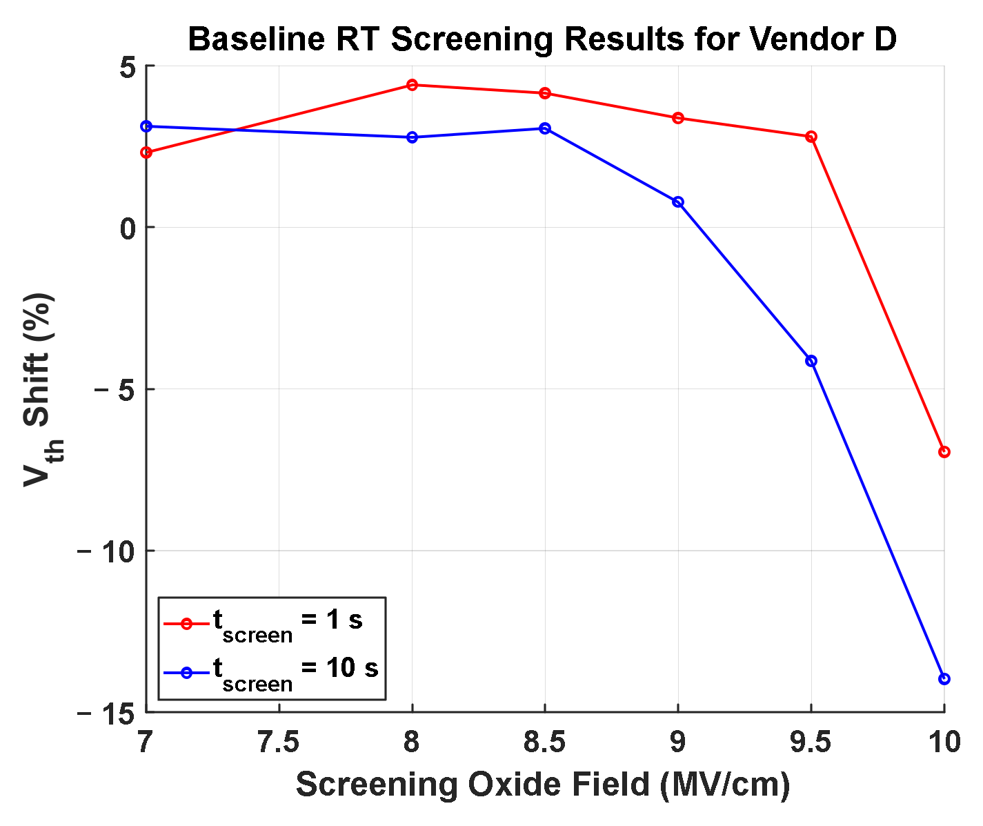
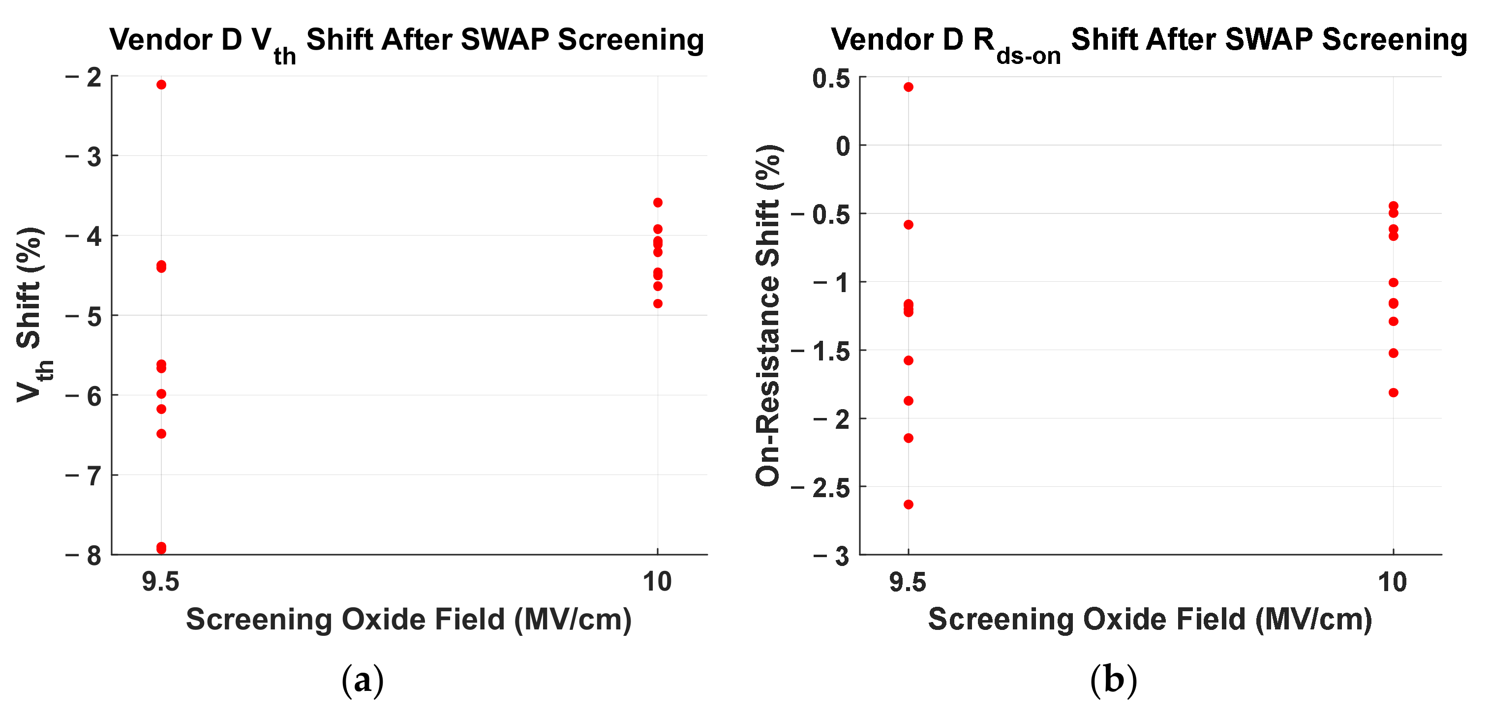
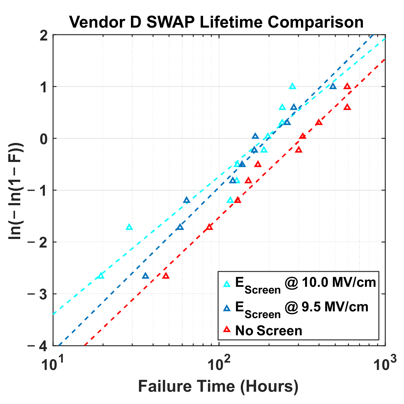
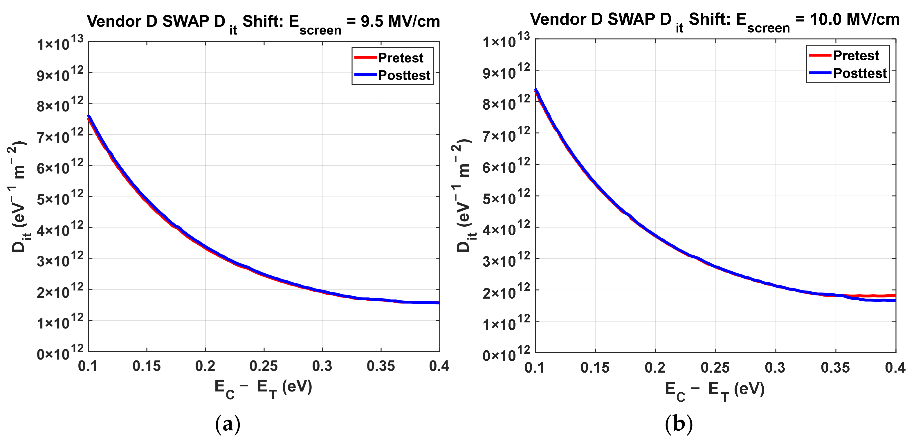
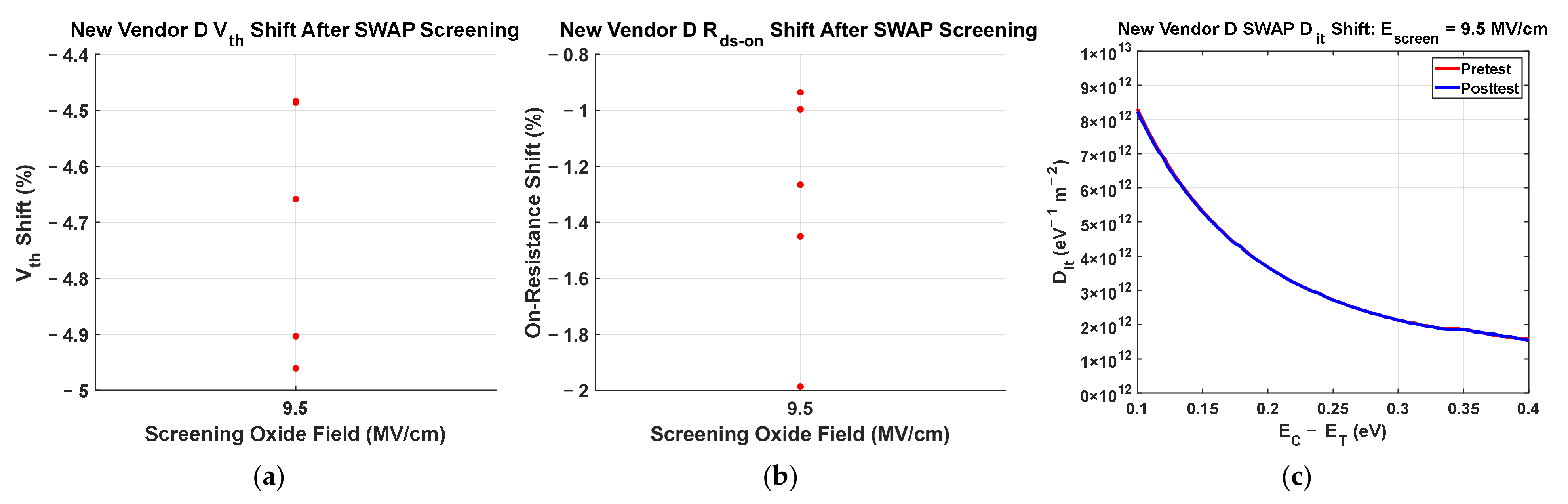
3.2. Results for Vendor D

The baseline screening results in terms of ΔVth with respect to Escreen and tscreen are shown in Figure 10. While the hole trapping effects are obvious due to the drop-off of ΔVth starting around Eox of 9.5 MV/cm, the field required is slightly higher than the devices from Vendor F. Table 3 shows the selected SWAP conditions for the devices from Vendor D. Notably, the time needed to adjust the Vth to within the acceptable ranges is longer for Vendor D than Vendor F, even with the same initial screening pulse conditions, and especially so for Escreen of 10 MV/cm.
Figure 11a,b show the distribution of ΔVth and ΔRds-on for each screening condition, respectively, for Vendor D. While the ΔRds-on is within the ±5% desired range, the ΔVth at Escreen = 9.5 MV/cm has some values that fall outside. Additionally, from Figure 12, both conditions end up degrading the device’s intrinsic lifetime as seen by the leftward shift in the Weibull plots of the screened DUTs relative to the unscreened one. However, there is no significant Dit increase associated with either condition, as shown with a representative sample in Figure 13a,b. Figure 11 and Figure 12 show that care must be taken in order to prevent significant device parameter shift or degradation, either by reducing Escreen or tscreen. Hence, a well calibrated SWAP process is essential to capture the benefits of the higher screening efficiency (due to higher Escreen) while preventing undesired ΔVth, ΔRds-on, and lifetime degradation.
To this end, new SWAP tests were recalibrated to the conditions shown in Table 4. Results shown in Figure 14a–c show acceptable ΔVth, ΔRds-on, and Dit shift in a representative sample. The current results are promising with ΔVth and ΔRds-on tightly within the ±5% range and no increase in the Dit. With the addition of the adjustment pulse, the number of variables for the screening treatment of the gate oxide doubles due to the extra pulse compared to single pulse gate screening. While this complicates the calibration significantly, the SWAP screening process can achieve more effective screening due to its higher Escreen in the initial screening pulse, making the calibration procedure rewarding in the long run from the decrease in extrinsic failures in the field.

3.3. Results for Vendor B
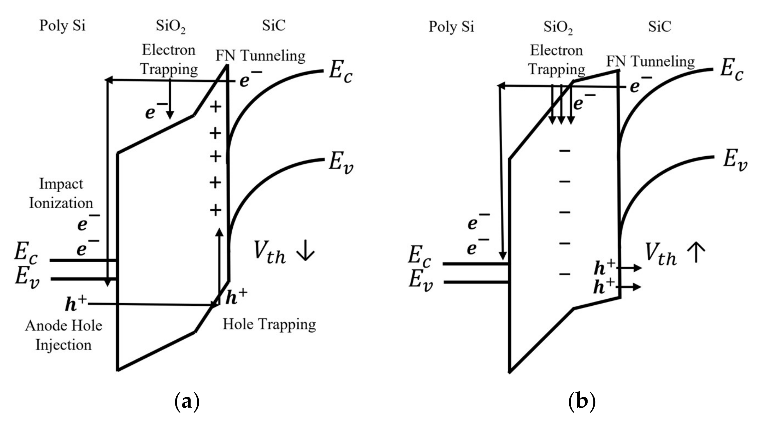
Figure 15 shows the baseline screening ΔVth results from Vendor B, which show the effects of hole trapping in the oxide starting around an Escreen of 8.5 MV/cm, with a significant drop at 9 MV/cm for tscreen of 10 s. As seen from Table 5, which shows the results of multiple SWAP calibration attempts, it is much harder to adjust the ΔVth after screening for Vendor B compared to the DUTs from Vendor D and especially compared to Vendor F, even with less aggressive SWAP conditions. Similar to Vendor D, this could be due to the higher screening voltages applied from the manufacturer due its higher oxide thickness. The devices from Vendor B have the thickest gate oxide out of all three vendors, and these devices proved to be the hardest to calibrate for the SWAP technique. Additionally, the gate oxides of the DUTs from Vendor B are deposited, rather than thermally grown as in the devices from Vendor D and Vendor F. It is known that SiC trench MOSFETs tend to have higher Dit due to the trench wall etching process and lower quality gate oxide. This increase in the interface traps leads to more charge trapping, which can cause the ΔVth to increase [18,19,20]. For all SWAP conditions tested, none stayed within the desired ±5% ΔVth range.
Figure 16 shows the effects of each step in the SWAP process on the device ΔVth for a given tscreen of 10 s, Eadj of 8, and tadj of 2 s. As shown, it is apparent that the effects of the adjustment pulse are only very effective for devices screened at higher fields. For Escreen at 8.5 MV/cm, the adjustment pulse has almost no effect on the ΔVth, and so there is no point is setting Escreen lower for SWAP. For Escreen of 9 MV/cm and 9.5 MV/cm, the effects of the adjustment pulse are more apparent; however, even though more of the Vth can be recovered at higher Escreen, the significant ΔVth from hole injection in the oxide from the screening pulse completely negates the beneficial effects of the adjustment pulse. Therefore, similar to the devices from Vendor D, care must be taken to reduce either the Escreen or tscreen in order to preserve the device characteristics.

4. Discussion

The methodology of the adjustment pulse after screening is based on the charge trapping phenomenon in the SiC MOSFET gate oxide during the screening process [14,15,21]. At high oxide electric fields (Eox > ~9 MV/cm), the electrons from the SiC tunnel through the oxide due to the high field, causing impact ionization in the polysilicon gate of the SiC MOSFET as shown in Figure 17a [5,22]. During impact ionization, the electrons are swept out of the device, while the holes are injected into the oxide due to the high Eox in a process known as anode hole injection, with some holes trapped near the interface in the oxide. This net positive charge in the gate oxide causes the threshold voltage to decrease. On the other hand, at lower oxide electric fields (Eox < ~9 MV/cm), the electrons from the SiC do not have the energy to cause impact ionization in the gate, and so more electrons than holes are trapped in the gate oxide due to the elimination of anode hole injection, as shown in Figure 17b [14]. This causes a net negative charge in the gate oxide, which increases the threshold voltage.
During the initial screening pulse of SWAP, the Escreen is high enough to cause impact ionization and anode hole injection. This causes the initial Vth to shift down after the screening pulse, as shown in Figure 17a. Then, the adjustment pulse is applied, which only injects electrons. This secondary pulse also causes some of the trapped holes to detrap from the oxide. The combined effects of this cause the threshold voltage to increase again, as shown in Figure 17b. By balancing the effects of electron and hole trapping within the oxide, the screening and adjustment pulses can be tuned in order to reduce the total ΔVth during the screening process [11]. Proper calibration by tweaking the initial Escreen and tscreen is needed to prevent significant shift in device characteristics (ΔVth, ΔRds-on, Dit, and lifetime). By reaching for the maximum possible screening field and time, the overall screening efficiency is improved, and the risk of extrinsic failure in the field for the SiC MOSFETs is reduced.
In order to confirm that the gate oxide of the DUTs is not locally damaged during the SWAP process, a pre-screen and post-recovery gate leakage current measurement at Vgs = 20 V is performed and compared for Vendors F and D, as shown in Figure 18a,b, respectively. If possible damage to the gate oxide would not be observable by measuring the Vth, Rds-on, and intrinsic lifetime, any damage to the oxide may be observable via a gate leakage current measurement [23]. Although this is not considered a calibration step, this measurement was performed in order to ensure that the post-recovery gate oxide is relatively healthy. As shown, there is no change in the gate leakage currents for both vendors for all testing conditions. If any significant damage to the gate happened during the SWAP process, then the leakage current after the screening and recovery process would be increased post-recovery [23]. However, there was no change in the device leakage currents, meaning that such damage did not occur.
Due to the random nature of extrinsic defects, a direct comparison between SWAP and other screening techniques based on screen-out performance will be very difficult without a very large sample size [24]. Compared to the traditional short high-voltage screening method, the SWAP method allows manufacturers to apply a higher screening voltage for a specific gate oxide thickness but reducing the amount of threshold voltage shift due to hole injection, which in turn increases the screening efficiency [6,14]. Compared to the long-term burn-in method, the SWAP method firstly applies a much higher screening voltage, while also being a much shorter process to complete (~5 s for SWAP versus many minutes to hours for burn-in) [6,24]. This allows manufacturers to increase the throughput of their device screening processes while also maintaining a high level of screening efficiency.

5. Conclusions

In this paper, the effects of the gate oxide screening with adjustment pulse (SWAP) procedure on the devices from Vendors F, D, and B are presented. Based on the results, with a well calibrated process such as that carried out for Vendor F, the ΔVth caused by gate oxide screening at high Eox (>~9 MV/cm) can be adjusted to within acceptable values. Additionally, it should not significantly degrade the device Rds-on or Dit, or reduce the device’s intrinsic lifetime. Improperly calibrated SWAP screening can lead to unwanted changes in device characteristics and lifetime that cannot be outweighed by the benefits of higher Escreen, so care must be taken to ensure that the SWAP conditions are determined carefully. While no universal optimization method for multiple SiC MOSFET technologies is presented, this work shows that it is possible to reduce the ΔVth due to high field oxide screening by properly calibrating the SWAP conditions for a set of devices. Although the initial calibration of the screening method is much more rigorous than a single pulse screening process, by accounting for some of the negative Vth shift with the adjustment pulse, SWAP allows manufacturers to screen at higher Escreen than before, increasing the screening efficiency. This leads to a reduction in devices with extrinsic defects entering the field, reducing the failure rate of the SiC MOSFETs in operation.

Author Contributions

Conceptualization, M.J.; methodology, M.J. and M.B.; software, M.J. and M.B.; validation, M.J., M.B. and H.Y.; formal analysis, M.J., M.B., H.Y., J.Q., S.H., A.S., M.H.W. and A.K.A.; investigation, M.J. and M.B.; resources, M.J. and M.B.; data curation, M.J.; writing—original draft preparation, M.J.; writing—review and editing, M.J., M.B. and H.Y.; visualization, M.J. and M.B.; supervision, H.Y., A.S., M.H.W. and A.K.A.; project administration, A.S. and A.K.A.; funding acquisition, A.S. and A.K.A. All authors have read and agreed to the published version of the manuscript.

Funding

This research was funded by the Ford Motor Company under grant number GR136168.

Data Availability Statement

Data are contained within the article.

Conflicts of Interest

Author Atsushi Shimbori is employed by the Ford Motor Co. The remaining authors declare that the research was conducted in the absence of any commercial or financial relationships that could be construed as potential conflicts of interest. The authors declare that this study received funding from the Ford Motor Company. The funders had no role in the design of the study; in the collection, analyses, or interpretation of data; in the writing of the manuscript; or in the decision to publish the results.

Abbreviations

The following abbreviations are used in this manuscript:
SWAPScreening With Adjustment Pulse
TDDBTime Dependent Dielectric Breakdown
MOSFETMetal-Oxide-Semiconductor Field Effect Transistor
SiCSilicon Carbide
DUTDevice Under Test

References

  1. Tsunenobu, K.; James, A.C. Physical Properties of Silicon Carbide. In Fundamentals of Silicon Carbide Technology: Growth, Characterization, Devices and Applications; Wiley-IEEE: Piscataway, NJ, USA, 2014; pp. 11–38. [Google Scholar]
  2. Hamada, K.; Nagao, M.; Ajioka, M.; Kawai, F. SiC—Emerging Power Device Technology for Next-Generation Electrically Powered Environmentally Friendly Vehicles. IEEE Trans. Electron Devices 2015, 62, 278–285. [Google Scholar] [CrossRef]
  3. Tan, C.; Stecca, M.; Soeiro, T.B.; Dong, J.; Bauer, P. Performance Evaluation of an Electric Vehicle Traction Drive Using Si/SiC Hybrid Switches. In Proceedings of the 2021 IEEE 19th International Power Electronics and Motion Control Conference (PEMC), Gliwice, Poland, 25–29 April 2021; pp. 278–283. [Google Scholar]
  4. Wang, J.; Jiang, X. Review and analysis of SiC MOSFETs’ ruggedness and reliability. IET Power Electron. 2020, 13, 445–455. [Google Scholar] [CrossRef]
  5. Liu, T.; Zhu, S.; White, M.H.; Salemi, A.; Sheridan, D.; Agarwal, A.K. Time-Dependent Dielectric Breakdown of Commercial 1.2 kV 4H-SiC Power MOSFETs. IEEE J. Electron Devices Soc. 2021, 9, 633–639. [Google Scholar] [CrossRef]
  6. Aichinger, T.; Schmidt, M. Gate-oxide reliability and failure-rate reduction of industrial SiC MOSFETs. In Proceedings of the 2020 IEEE International Reliability Physics Symposium (IRPS), Dallas, TX, USA, 28 April–30 May 2020; pp. 1–6. [Google Scholar]
  7. Cheung, K.P. SiC power MOSFET gate oxide breakdown reliability—Current status. In Proceedings of the 2018 IEEE International Reliability Physics Symposium (IRPS), Burlingame, CA, USA, 11–15 March 2018; pp. 2B.3-1–2B.3-5. [Google Scholar]
  8. Zheng, Y.; Potera, R.; Witt, T. Characterization of Early Breakdown of SiC MOSFET Gate Oxide by Voltage Ramp Tests. In Proceedings of the 2021 IEEE International Reliability Physics Symposium (IRPS), Monterey, CA, USA, 21–25 March 2021; pp. 1–5. [Google Scholar]
  9. Beier-Moebius, M.; Lutz, J. Breakdown of gate oxide of 1.2 kV SiC-MOSFETs under high temperature and high gate voltage. In Proceedings of the PCIM Europe 2016, International Exhibition and Conference for Power Electronics, Intelligent Motion, Renewable Energy and Energy Management, Nuremberg, Germany, 10–12 May 2016; pp. 1–8. [Google Scholar]
  10. Lee, J.C.; Chen, I.-C.; Hu, C. Modeling and characterization of gate oxide reliability. IEEE Trans. Electron Devices 1988, 35, 2268–2278. [Google Scholar] [CrossRef]
  11. Jin, M.; Bhattacharya, M.; Shi, L.; Qian, J.; Houshmand, S.; Yu, H.; White, M.H.; Agarwal, A.K.; Liu, T.; Zhu, S.; et al. Threshold Voltage Adjustment of Commercial SiC MOSFETs During Gate Oxide Screening by Low Field Pulse. In Proceedings of the 2024 IEEE 11th Workshop on Wide Bandgap Power Devices & Applications (WiPDA), Dayton, OH, USA, 4–6 November 2024; pp. 1–5. [Google Scholar]
  12. Berens, J.; Aichinger, T. A Straightforward Electrical Method to Determine Screening Capability of GOX Extrinsics in Arbitrary, Commercially Available SiC MOSFETs. In Proceedings of the 2021 IEEE International Reliability Physics Symposium (IRPS), Monterey, CA, USA, 21–25 March 2021; pp. 1–5. [Google Scholar]
  13. Miki, H.; Sagawa, M.; Mori, Y.; Murata, T.; Kinoshita, K.; Asaka, K.; Oda, T. Accurate Screening of Defective Oxide on SiC Using Consecutive Multiple Threshold—Voltage Measurements. In Proceedings of the 2022 IEEE International Reliability Physics Symposium (IRPS), Dallas, TX, USA, 27–31 March 2022; pp. 8B.2-1–8B.2-7. [Google Scholar]
  14. Shi, L.; Zhu, S.; Qian, J.; Jin, M.; Bhattacharya, M.; White, M.H.; Agarwal, A.K.; Shimbori, A.; Liu, T. Investigation of different Screening Methods on Threshold Voltage and Gate Oxide Lifetime of SiC Power MOSFETs. In Proceedings of the 2023 IEEE International Reliability Physics Symposium (IRPS), Monterey, CA, USA, 26–30 March 2023; pp. 1–7. [Google Scholar]
  15. Maaß, S.; Reisinger, H.; Aichinger, T.; Rescher, G. Influence of High-Voltage Gate-Oxide Pulses on the BTI Behavior of SiC MOSFETs. In Proceedings of the 2020 IEEE International Reliability Physics Symposium (IRPS), Dallas, TX, USA, 28 April–30 May 2020; pp. 1–6. [Google Scholar]
  16. Noguchi, M.; Koyama, A.; Iwamatsu, T.; Amishiro, H.; Watanabe, H.; Miura, N. Gate Oxide Instability and Lifetime in SiC MOSFETs under a Wide Range of Positive Electric Field Stress. In Proceedings of the 2020 IEEE International Electron Devices Meeting (IEDM), San Francisco, CA, USA, 12–18 December 2020; pp. 23.24.21–23.24.24. [Google Scholar]
  17. Yu, S.; White, M.H.; Agarwal, A.K. Experimental Determination of Interface Trap Density and Fixed Positive Oxide Charge in Commercial 4H-SiC Power MOSFETs. IEEE Access 2021, 9, 149118–149124. [Google Scholar] [CrossRef]
  18. Asllani, B.; Castellazzi, A.; Salvado, O.A.; Fayyaz, A.; Morel, H.; Planson, D. VTH-Hysteresis and Interface States Characterisation in SiC Power MOSFETs with Planar and Trench Gate. In Proceedings of the 2019 IEEE International Reliability Physics Symposium (IRPS), Monterey, CA, USA, 31 March–4 April 2019; pp. 1–6. [Google Scholar]
  19. Berens, J.; Rasinger, F.; Aichinger, T.; Heuken, M.; Krieger, M.; Pobegen, G. Detection and Cryogenic Characterization of Defects at the SiO2/4H-SiC Interface in Trench MOSFET. IEEE Trans. Electron Devices 2019, 66, 1213–1217. [Google Scholar] [CrossRef]
  20. Tian, K.; Hallén, A.; Qi, J.; Nawaz, M.; Ma, S.; Wang, M.; Guo, S.; Elgammal, K.; Li, A.; Liu, W. Comprehensive Characterization of the 4H-SiC Planar and Trench Gate MOSFETs From Cryogenic to High Temperature. IEEE Trans. Electron Devices 2019, 66, 4279–4286. [Google Scholar] [CrossRef]
  21. Lelis, A.J.; Green, R.; Habersat, D.B. SiC MOSFET reliability and implications for qualification testing. In Proceedings of the 2017 IEEE International Reliability Physics Symposium (IRPS), Monterey, CA, USA, 2–6 April 2017; pp. 2A-4.1–2A-4.4. [Google Scholar]
  22. Rescher, G.; Pobegen, G.; Grasser, T. Threshold Voltage Instabilities of Present SiC-Power MOSFETs under Positive Bias Temperature Stress. Mater. Sci. Forum 2016, 858, 481–484. [Google Scholar] [CrossRef]
  23. Ouaida, R.; Berthou, M.; León, J.; Perpiñà, X.; Oge, S.; Brosselard, P.; Joubert, C. Gate Oxide Degradation of SiC MOSFET in Switching Conditions. IEEE Electron Device Lett. 2014, 35, 1284–1286. [Google Scholar] [CrossRef]
  24. Chbili, Z.; Matsuda, A.; Chbili, J.; Ryan, J.T.; Campbell, J.P.; Lahbabi, M.; Ioannou, D.E.; Cheung, K.P. Modeling Early Breakdown Failures of Gate Oxide in SiC Power MOSFETs. IEEE Trans. Electron Devices 2016, 63, 3605–3613. [Google Scholar] [CrossRef]
Figure 1. (a) Examples of extrinsic defects in the SiC MOSFET gate oxide [6]; (b) Weibull plot with extrinsic tail from a constant voltage TDDB test for Vendor F [11].
Electronics 14 01366 g001
Figure 2. (a) Structure of a planar SiC MOSFET; (b) structure of an asymmetric trench SiC MOSFET.
Electronics 14 01366 g002
Figure 3. Testing procedure for screening with adjustment pulse (SWAP).
Electronics 14 01366 g003
Figure 4. Pretest threshold voltage for Vendors B, F, and D.
Electronics 14 01366 g004
Figure 5. Baseline room temperature gate oxide screening threshold voltage shift for Vendor F.
Electronics 14 01366 g005
Figure 6. Adjustment pulse length calibration for Vendor F with respect to screening pulse oxide field. The tscreen was held at 10 s, and Eadj was held at 8 MV/cm.
Electronics 14 01366 g006
Figure 7. (a) Vendor F Vth shift due to SWAP screening; (b) Vendor F Rds-on shift due to SWAP screening.
Electronics 14 01366 g007
Figure 8. TDDB Weibull plots from Vendor F with different Escreen conditions compared to a sample of unscreened devices.
Electronics 14 01366 g008
Figure 9. Vendor F energy dependent Dit distribution before and after screening by SWAP with Escreen of (a) 9.0 MV/cm; (b) 9.5 MV/cm; (c) 10.0 MV/cm.
Electronics 14 01366 g009
Figure 10. Baseline room temperature gate oxide screening threshold voltage shift for Vendor D.
Electronics 14 01366 g010
Figure 11. (a) Vendor D Vth shift due to SWAP screening; (b) Vendor D Rds-on shift due to SWAP screening.
Electronics 14 01366 g011
Figure 12. TDDB Weibull plots from Vendor D with different Escreen conditions compared to a sample of unscreened devices.
Electronics 14 01366 g012
Figure 13. Vendor D energy-dependent Dit distribution before and after screening by SWAP with Escreen of (a) 9.5 MV/cm; (b) 10.0 MV/cm.
Electronics 14 01366 g013
Figure 14. Parameter shifts for recalibrated SWAP conditions for Vendor D: (a) Vth shift due to SWAP screening; (b) Rds-on shift due to SWAP screening; (c) Dit shift due to SWAP screening.
Electronics 14 01366 g014
Figure 15. Baseline room temperature gate oxide screening threshold voltage shift for Vendor B.
Electronics 14 01366 g015
Figure 16. Threshold voltage of devices from Vendor B at each point in the SWAP process for three different Escreen. The tscreen is 10 s, Eadj is 8 MV/cm, and tadj is 2 s.
Electronics 14 01366 g016
Figure 17. (a) Band diagram of the SiC MOSFET gate structure at high Eox (>~9 MV/cm) during the first pulse of SWAP; (b) band diagram of the SiC MOSFET gate structure at low Eox (<~9 MV/cm) during the second pulse of SWAP.
Electronics 14 01366 g017
Figure 18. (a) Gate leakage currents for Vendor F before screening (red) and after recovery (blue); (b) gate leakage currents for Vendor D before screening (red) and after recovery (blue).
Electronics 14 01366 g018
Table 1. Details of the DUTs from Vendor F, D, and B.
VendorVendor FVendor DVendor B
StructurePlanarPlanarAsymmetric Trench
Voltage Rating1200 V1200 V1200 V
Current Rating7.6 A20 A4.7 A
Average Oxide Vbr @ 150 °C42 V54.3 V62.8 V
Estimated tox38.2 nm49.4 nm57.1 nm
Table 2. SWAP conditions for Vendor F.
Escreen (MV/cm)tscreen (s)Eadj (MV/cm)tadj (s)
91082
9.51082
101082
Table 3. SWAP conditions for Vendor D.
Escreen (MV/cm)tscreen (s)Eadj (MV/cm)tadj (s)
9.51085
10108.5200
Table 4. New SWAP conditions for Vendor D.
Escreen (MV/cm)tscreen (s)Eadj (MV/cm)tadj (s)
9.5582
Table 5. Attempted SWAP conditions for Vendor B.
Escreen (MV/cm)tscreen (s)Eadj (MV/cm)tadj (s)ΔVth (%)
8.51082−7.7
8.51084−8.4
91082−44
910810−37
95810−27
957.510−30
9.51082−32
9.51810−42
Disclaimer/Publisher’s Note: The statements, opinions and data contained in all publications are solely those of the individual author(s) and contributor(s) and not of MDPI and/or the editor(s). MDPI and/or the editor(s) disclaim responsibility for any injury to people or property resulting from any ideas, methods, instructions or products referred to in the content.

