1. Introduction
In recent years, the explosive growth of 5G communication technology has significantly transformed global network infrastructure [
1]. Compared to previous generations, 5G stands out with its higher transmission speeds, extremely low latency, and the ability to connect MA sieve IoT devices [
2]. To support these advancements, 5G networks utilize both Sub-6 GHz and millimeter-wave frequency bands [
3]. However, the expansion into broader frequency ranges, along with higher device density, has heightened the challenges posed by electromagnetic interference (EMI) [
4,
5]. This interference, especially in dense 5G network environments with numerous base stations and devices, presents major obstacles to signal quality and system stability [
6]. In complex 5G scenarios, EMI can lead to signal degradation, progress to data loss, and eventually result in attenuation, which ultimately jeopardizes the reliability of communication systems. Furthermore, EMI and electromagnetic radiation pose potential health risks to humans [
7,
8,
9]. As a result, the development of efficient electromagnetic compatibility (EMC) technologies has become a critical area of research to mitigate interference, protect human health, and ensure reliable signal transmission. Among these EMC solutions, microwave absorbers (MAs) play a pivotal role by absorbing electromagnetic waves to reduce reflection and interference, thereby addressing EMI problems [
10]. Recently, ultra-wideband microwave absorbers have gained significant attention due to their capability to cover a wide frequency spectrum, making them particularly effective for EMI suppression in complex electromagnetic environments, including those seen in 5G communications. These absorbers provide a robust solution for mitigating interference across diverse frequency bands, greatly contributing to the resolution of EMI challenges in 5G systems.
In previous studies, ferrite materials, metal alloys, and carbon-based materials were commonly used for microwave absorbers (MAs), each with its unique advantages. Ferrites and metal alloys offer excellent broadband absorption, especially at lower frequency [
11,
12]. However, they tend to be dense, heavy, and costly, with limited high-frequency absorption [
13]. Carbon-based materials show promise due to their tunability, environmental stability, and low density [
14]. For example, Jie Luo et al. developed a CNT-carbon black hybrid absorber, achieving over 90% absorption across 5.8–18 GHz with an absorption rate exceeding 96.3% [
15]. However, the optical transparency and high-frequency absorption efficiency of substrate materials used in traditional microwave absorbers (MAs) have not been fully considered. As a result, these absorbers are unsuitable for applications requiring both high microwave absorption and optical transparency. This has led to growing interest in optically transparent broadband absorbers. Transparent conductive films, known for their thinness, high optical transparency, and excellent conductivity, have become the preferred materials for optically transparent ultra-wideband MAs [
16,
17,
18,
19]. For instance, Jang et al. developed a transparent MA using an aluminum grid structure, achieving enhanced absorption performance between 5.8 and 12.2 GHz [
20]. Similarly, Ling et al. designed a multi-layer transparent conductive film-based MA with absorption rates exceeding 90% over 38–142 GHz and a relative bandwidth of 115.5% [
21]. The development of indium tin oxide (ITO) films has significantly advanced the performance of optically transparent MAs. By combining highly conductive ITO films with flexible, transparent substrates like polymethyl methacrylate (PMMA) and polyethylene terephthalate (PET), these absorbers can achieve high levels of optical transparency [
22,
23,
24,
25,
26]. HAO et al. proposed and validated a flexible multilayer structure for a transparent ultra-wideband MA, exhibiting superior optical transparency and microwave absorption, with a relative bandwidth of 159% where absorption exceeds 90% [
27]. Zhang et al. developed and tested an ITO-based MA with a windmill-shaped pattern using PMMA and PET substrates, showing optical transparency and absorption rates greater than 90% over the 8.3–17.4 GHz range [
28]. The metasurface structure composed of transparent media and resistive films demonstrates exceptional performance in broadband absorption, making it an ideal candidate for flexible, transparent, lightweight, and broadband microwave absorbers [
29,
30]. It effectively replaces traditional microwave absorbers, addressing the challenges of high-demand microwave absorption scenarios and applications requiring high optical transparency. Researchers have continually sought more efficient absorber design schemes, and traditional “sandwich” absorber structures, commonly employed in earlier designs, offer acceptable absorption capacity but often face challenges in further optimizing absorption bandwidth. To address this limitation, the multi-layer stacked absorber structure has emerged as a prominent research focus in recent years. By strategically stacking multiple lossy layers and selecting suitable dielectric materials, this advanced design approach achieves enhanced absorption performance while maintaining excellent optical transparency and wide-angle stability.
In this design, PET and PMMA are used as dielectric substrate materials. Due to their good optical transparency and flexibility, compared with traditional absorbent materials, they are easier to prepare, more in line with the concept of environmental protection, with low production cost and smaller overall thickness [
31,
32,
33]. By choosing their dielectric constants reasonably, a multi-layer absorber design is realized by stacking them according to a certain sequence gradient, which provides an efficient design scheme for UWB absorber designs. The multi-layer stacking mode of PMMA-ITO-PET is adopted in the design scheme and the ITO resistive film is meticulously patterned and etched onto the PET substrate. A mesh grid structure is used for the backing and a multi-layer stacking approach ensures the optical transparency of the overall MA structure within the visible spectrum. Full-wave simulations using HFSS confirm optimal impedance matching, crucial for high-efficiency absorption. Simulation results indicate that the absorber achieves over 90% absorption across 4.07–25.02 GHz, covering key bands such as C, X, Ku, and parts of the K-band, with a relative bandwidth (RBW) of 144%, demonstrating its ultra-wideband capabilities. The design also features excellent angle stability; under TE polarization, it maintains over 90% absorption bandwidth for angles between 0° and 45°, with RBW exceeding 120%, and at angles up to 60°, absorption exceeds 80%. For TM polarization, the structure achieves over 90% absorption with RBW above 125% for angles up to 60° and at 70°, it maintains over 85% absorption with RBW over 120%. This design offers superior broadband absorption, strong polarization insensitivity, and high angle stability, making it ideal not only for mitigating EMI in 5G base stations and devices but also for applications in electromagnetic stealth and electromagnetic compatibility (EMC) in electronic systems.
2. Structural Design and Simulation
To enhance the optical transparency and conformability of the overall structure, this design adopts flexible transparent metamaterials—PMMA and PET—as substrate materials.
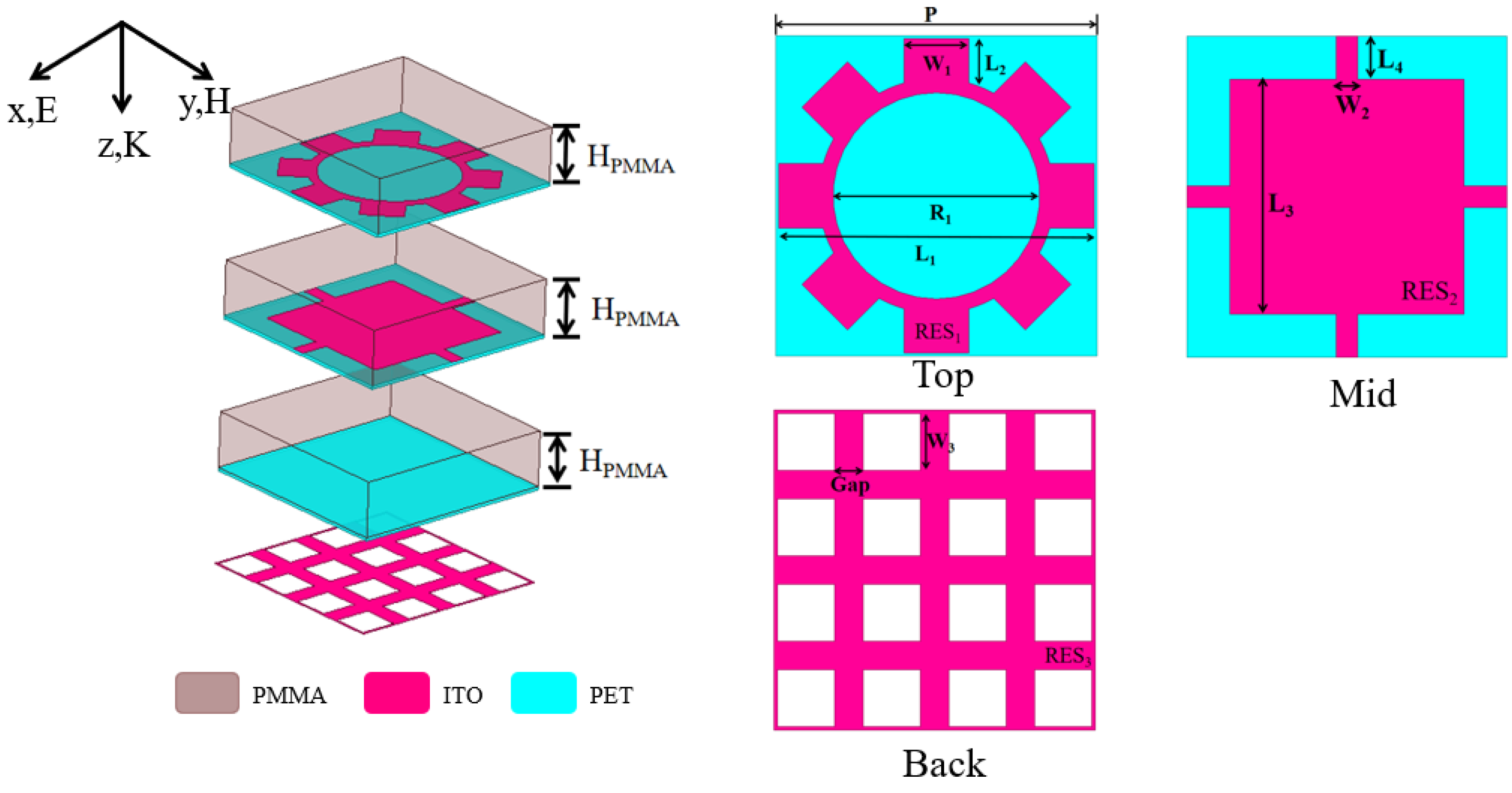
Figure 1 shows the designed ultra-wideband absorber unit structure with three ITO resonant layers. The ITO resistive film, with a thickness of 45 nm, is sufficiently thin to be considered negligible in the overall structural dimensions. The unit structure comprises three stacked layers, referred to as the upper, middle, and lower layers. Each layer consists of a PMMA substrate, a PET substrate, and an ITO resistive film. On the upper and middle layers, the ITO resonant patterns are etched onto the PET substrates. This configuration aims to establish impedance matching and interlayer coupling, enhance design flexibility, and achieve broadband wave absorption.
In microwave design, it is well established that resonators with large perimeters and narrow linewidths can provide significant inductance, while small gaps between adjacent loops generate substantial capacitance [
34]. Accordingly, the top-layer ITO resonator incorporates a circular ring with protruding square elements along its circumference to precisely tune the capacitance and inductance of the composite structure. A similar design principle was applied to the middle-layer ITO resonator. Through iterative optimization of geometric parameters (e.g., ring diameter, gap spacing) and sheet resistance, the extracted equivalent circuit parameters were adjusted to approach ideal values, achieving excellent impedance matching—a critical requirement for ultra-wideband absorption. Furthermore, by utilizing optically transparent PET/PMMA dielectric layers combined with a mesh grid-backed architecture, the metamaterial absorber (MA) demonstrates favorable optical transparency (>80% at 550 nm wavelength) [
35]. Therefore, the upper ITO resonant pattern is gear-shaped, while the middle ITO resonant pattern consists of a polygonal design composed of several rectangles. The ITO resistive film on the back plate is divided into a 4 × 4 mesh grid structure, which, compared to traditional rectangular back plates, enhances optical transparency by better integrating with the PET substrate. The ITO resonant patterns in the design exhibit sheet resistances of 100 Ω/sq, 60 Ω/sq, and 6 Ω/sq for the upper, middle, and lower layers, respectively. The relative permittivity values of the PMMA and PET substrates are 2.25 and 3, respectively, with loss tangents of 0.001 and 0.06. The thickness of each PMMA and PET substrate is set at 3 mm and 0.175 mm, respectively. The overall size is 9.525 mm (only 0.129 times the wavelength of the lowest cut-off frequency). Moreover, different resonant patterns in the MA design contribute distinct absorption effects. Optimal absorption efficiency is achieved by continuously refining the structural parameters to produce strong resonant effects.
The structural geometric parameters obtained through optimization are as follows: P = 11.25 mm, L
1 = 11.05 mm, L
2 = 1.57 mm, L
3 = 8.25 mm, L
4 = 1.5 mm, W
1 = 2.25 mm, W
2 = 0.75 mm, W
3 = 2 mm, Gap = 1 mm, and R
1 = 7.25 mm. They are summarized in
Table 1.
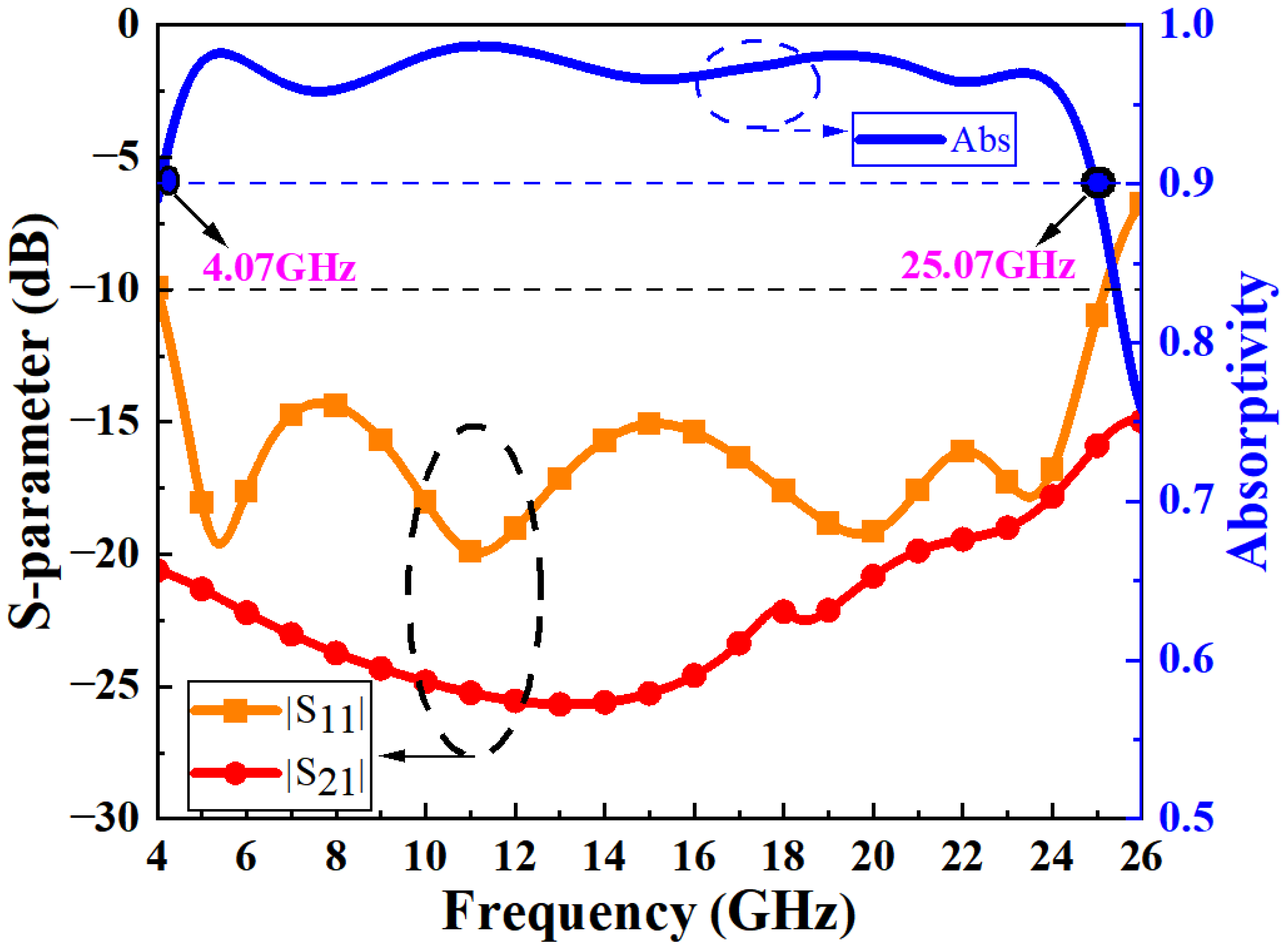
To further validate the proposed MA and its absorption characteristics, full-wave simulations were performed using HFSS(2019), an electromagnetic simulation software based on the finite element method. Periodic boundary conditions were applied in the x and y directions of the unit structure model within HFSS, allowing the electromagnetic plane wave to propagate along the +z-axis. The MA was excited by a Floquet port to simulate the model’s electromagnetic performance. The absorption rate can be calculated using the following formula:
Here, R(ω) represents the reflectivity and T(ω) represents the transmissivity. In the full-wave simulation analysis, these can be expressed as R(ω) = |S
11|
2, T(ω) = |S
21|
2.
Figure 2 shows the relevant S-parameter and absorption curves for normal incidence of electromagnetic waves. The simulation results reveal that the MA achieves an absorption bandwidth of 4.07–25.07 GHz, with absorption rates exceeding 90%. The relative bandwidth (RBW) can be defined as RBW = 2 × (f
max − f
min)/(f
max + f
min) × 100%, where f
max and f
min represent the upper and lower limits of the absorption band, respectively. The designed MA achieves an impressive RBW of 144%, covering multiple commonly used frequency bands, making it suitable for various operational environments. Its design flexibility also makes it ideal for applications such as electromagnetic shielding and radar stealth, effectively addressing electromagnetic pollution.
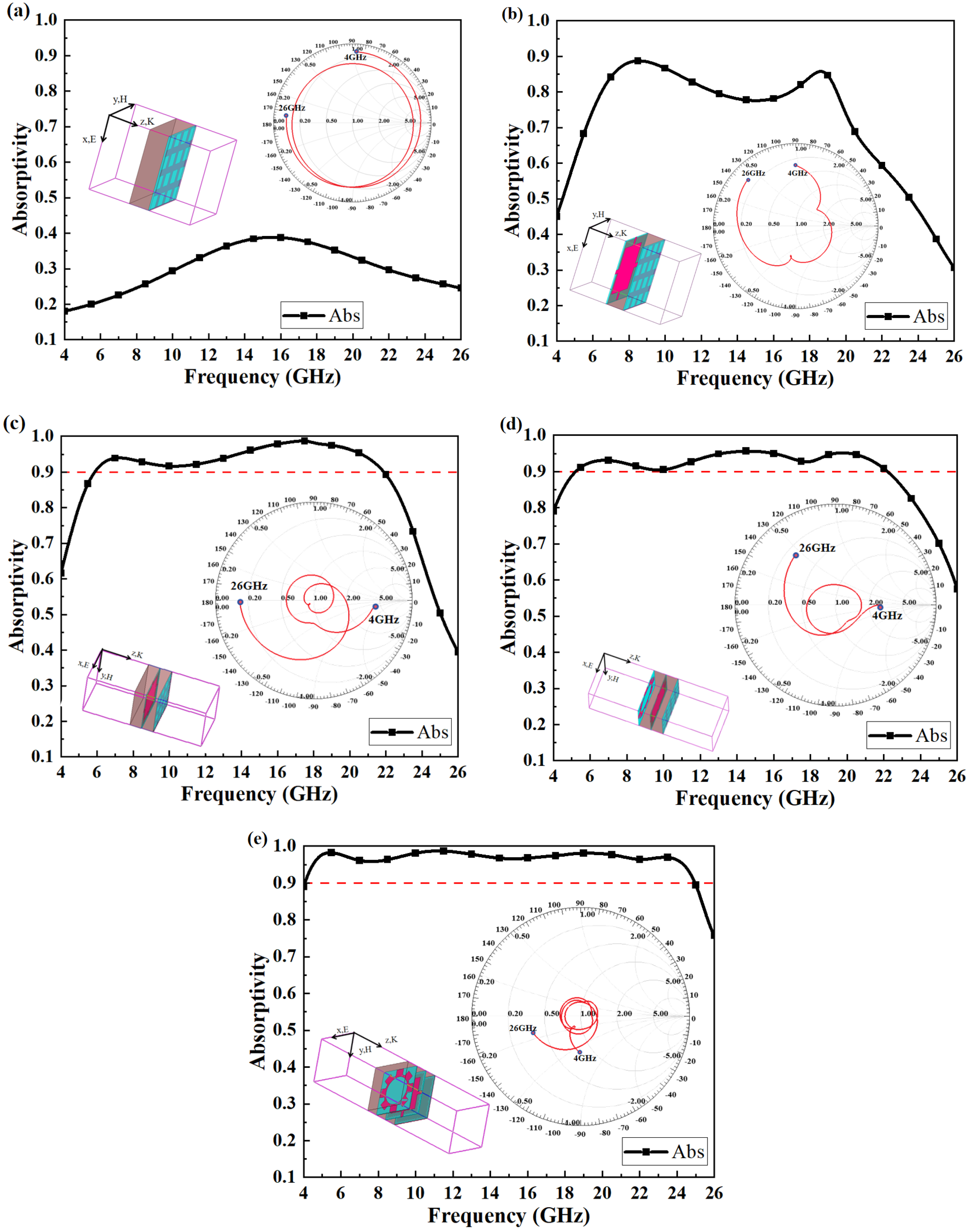
To better illustrate the impact of structural modifications on the absorption performance in this design,
Figure 3 provides a detailed depiction of how changes in the layered configuration affect the impedance. This also elucidates the step-by-step structural design process adopted in this work. From
Figure 3, it is evident that when the structure consists of only a single dielectric layer and a ground plane, the impedance curve tends toward a purely imaginary value, resulting in almost no absorption effect (
Figure 3a). Upon introducing the first ITO resonant pattern, the absorption curve rises significantly, indicating an improvement in the absorption performance (
Figure 3b). With the addition of the second PMMA dielectric layer, the impedance curve begins to exhibit a clear convergence trend (
Figure 3c), which corroborates our earlier assertion regarding the role of PMMA in enhancing the overall impedance matching of the structure. When the second ITO resonant pattern is incorporated, absorption in the low- and mid-frequency ranges improves significantly (
Figure 3d). Finally, with the addition of the third PMMA dielectric layer, the impedance curve achieves further convergence, leading to an absorption rate exceeding 90%. Across the simulated frequency band, the reflection coefficient of the structure remains below 0.1 and the absorption rate exceeds 0.9 (
Figure 3e). This demonstrates the critical contribution of each additional layer to the overall performance of the absorber. The final design, as shown in
Figure 1, achieves a remarkable ultra-wideband absorption effect, with absorption rates above 90% over a bandwidth of 4.07–25.02 GHz, resulting in a relative bandwidth (RBW) of 144%.
3. Results and Discussion
In the previous section, we analyzed the design of an ultra-wideband MA and
Table 1 shows the optimal geometric parameters obtained through optimization. By applying these optimal parameters, the ultra-wideband MA achieved an impressive 144% relative bandwidth (RBW). To further explore the microwave absorption mechanism, we will analyze the impedance matching and surface current distributions separately. According to transmission line theory, the reflection coefficient Γ can be expressed by the following formula:
Here, Z
eff represents the effective wave impedance of the metamaterial surface, while Z
0 = 377 Ω represents the impedance of free space. For the MA to achieve low reflectivity, Z
eff must equal Z
0 to realize ideal impedance matching, which is critical for achieving high absorption bandwidth. Furthermore, since the design utilizes a 6 Ω/sq ITO mesh grid backplate and, as shown in
Figure 2, S
21 is below −15 dB within the absorption bandwidth, S
21 can be approximated as 0. Therefore, the effective input impedance Z
eff of the proposed ultra-wideband MA can be expressed by Equation (3):
Here, μ
eff represents the effective permeability and ε
eff represents the effective permittivity. In electromagnetic analysis, normalized impedance is commonly used to describe how well the impedance matches that of free space. The normalized impedance can be calculated using the following formula:
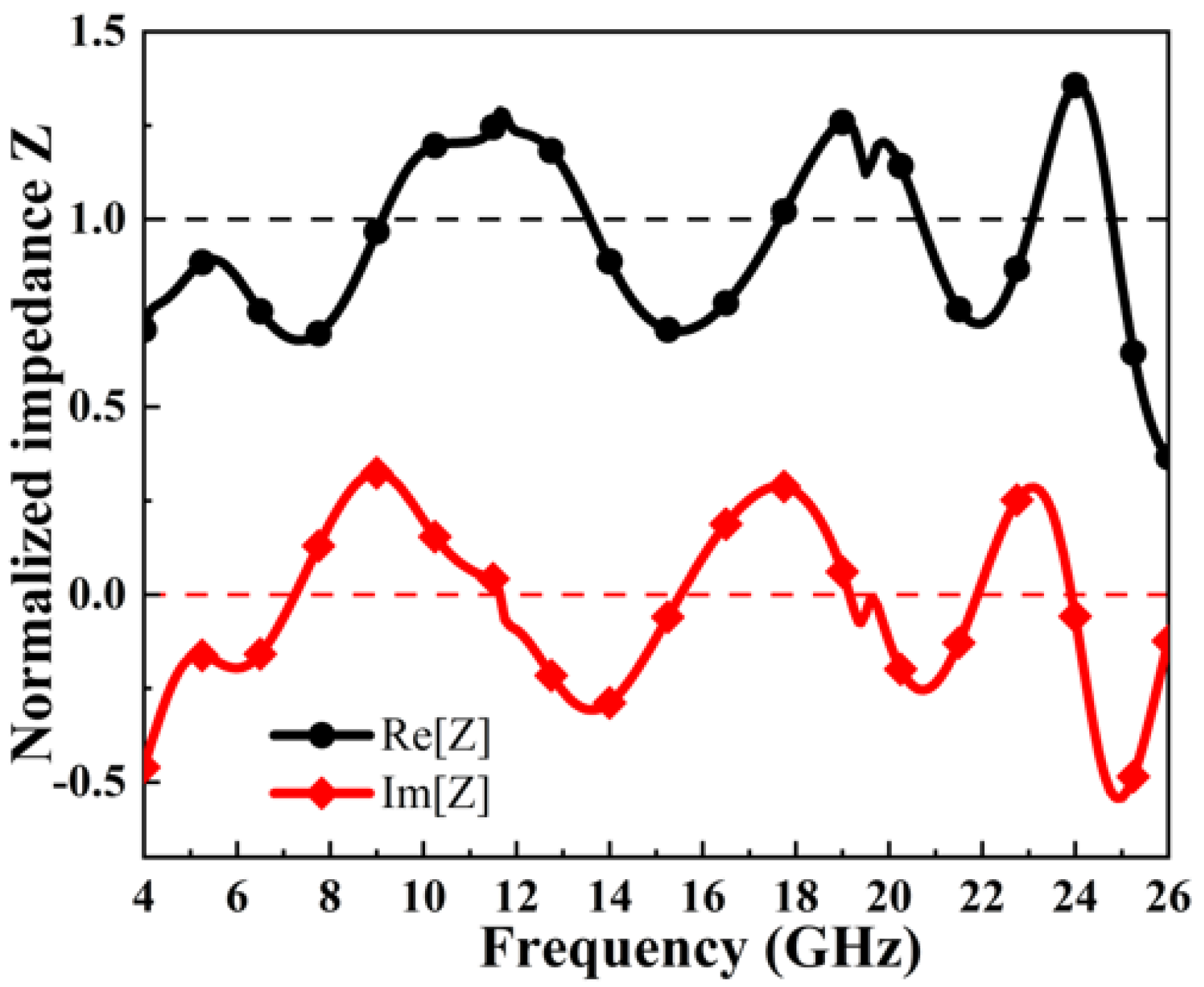
As shown in
Figure 4, within the absorption band (4.07–25.07 GHz), the real part of the normalized impedance fluctuates around 1 and the imaginary part fluctuates near 0. This indicates excellent impedance matching with free space, which is crucial for achieving ultra-wideband absorption. Additionally, as depicted in
Figure 2, the designed ultra-wideband MA exhibits four absorption peaks at 5.44 GHz, 11.18 GHz, 19.03 GHz, and 23.48 GHz. At these peaks, the real part of the impedance approaches 1 and the imaginary part approaches 0, resulting in near-zero reflectivity and absorption efficiency exceeding 98%.
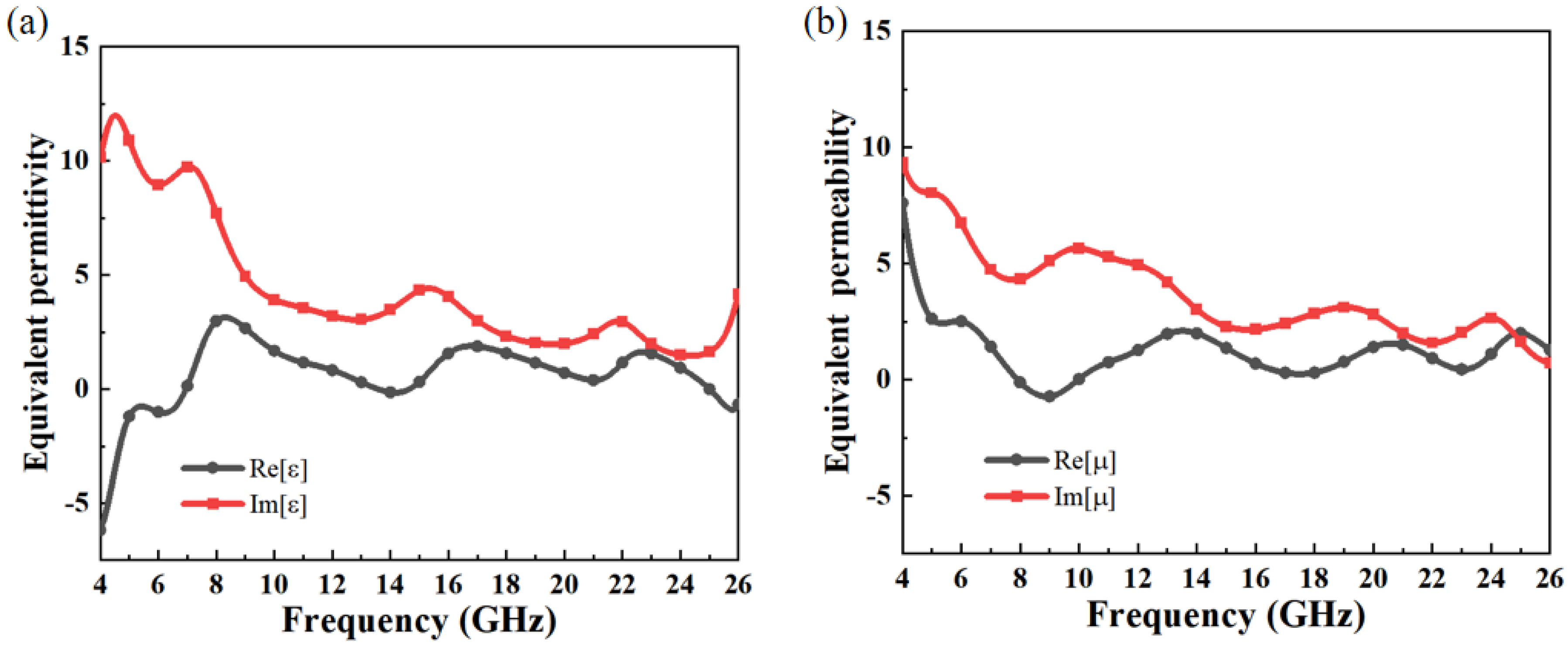
Since the designed metamaterial absorber (MA) exhibits an almost invariant electromagnetic response to the varying electromagnetic fields in free space, it can be regarded as a homogeneous medium, whose electromagnetic properties can be characterized by the effective permittivity (ε
eff) and effective permeability (μ
eff). This provides a more comprehensive explanation of the loss mechanism of electromagnetic waves within the designed MA. The effective permittivity and effective permeability can be calculated using Equations (5) and (6), respectively.
Here, k
0 represents the wave number in free space, j denotes the imaginary unit, and h refers to the overall thickness of the MA. The calculation results are shown in
Figure 5, where
Figure 5a,b illustrate the effective permittivity and relative permeability of the MA, respectively. It can be observed that within the absorption frequency band, the real parts of both parameters approach zero, and at the absorption peaks shown in
Figure 1, ε ≈ μ. By combining Equations (3) and (4), it can be concluded that impedance matching is achieved at the corresponding operational frequencies (5.44, 11.18, 19.03, and 23.48 GHz), resulting in an absorption efficiency exceeding 97%. Examining the imaginary parts of both parameters reveals that they are greater than zero within the working frequency range, indicating significant electromagnetic wave loss. This further demonstrates the excellent electromagnetic wave absorption capability of the designed MA.
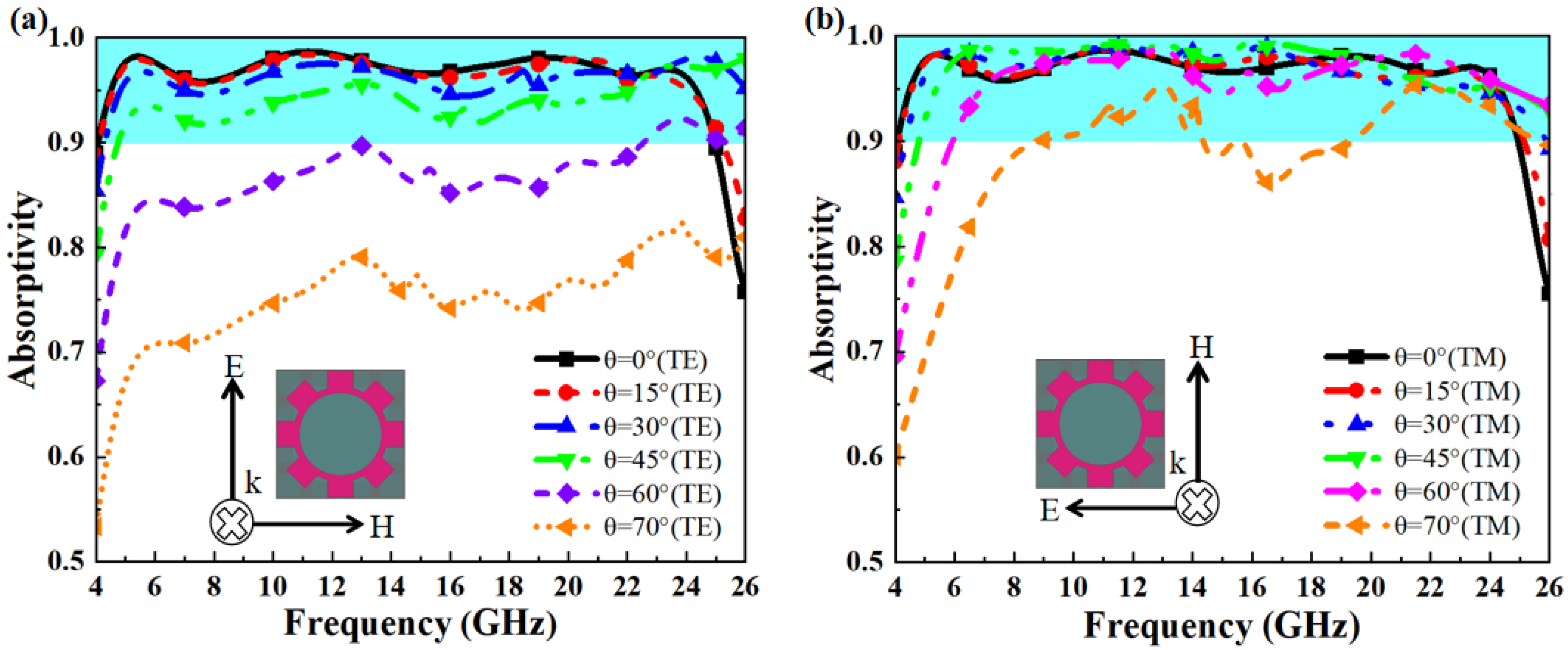
For ultra-wideband MAs, angle stability and polarization stability are crucial performance indicators to ensure adaptability to various electromagnetic wave incidences. As shown in
Figure 6a,b, the designed MA exhibits excellent angular stability in both TE and TM polarization modes, even as the oblique incidence angle increases. In TE mode,
Figure 6a demonstrates that the MA maintains over 90% absorption bandwidth across the 4–26 GHz band with an average RBW of over 130% for incident angles between 0 and 45°, and at 60°, it still achieves 80% absorption. Similarly, in the TM mode,
Figure 6b shows comparable performance to the TE mode, with superior absorption rates at higher angles (60–70°), maintaining over 90% absorption with an RBW exceeding 110%. Further, as demonstrated in
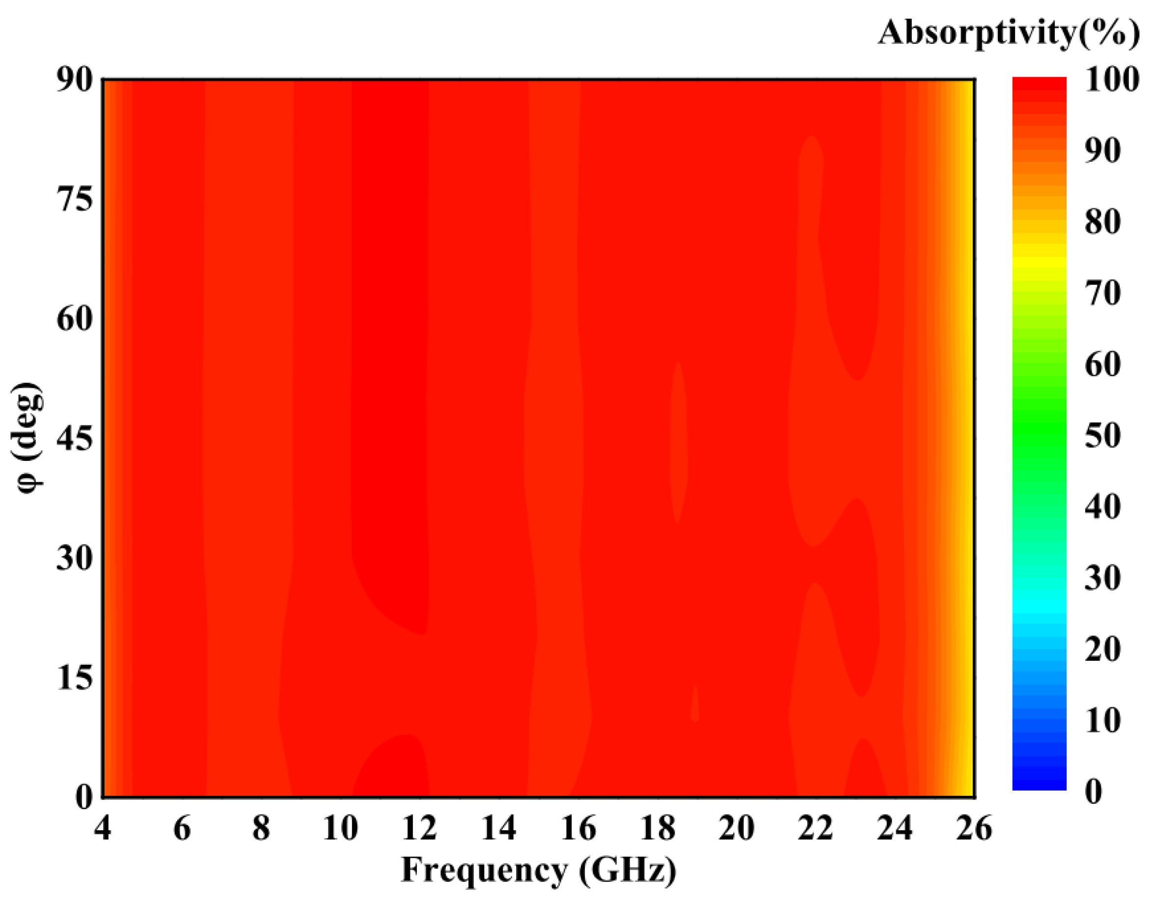
Figure 7, the MA absorption performance remains unaffected by changes in polarization angle under normal incidence. This behavior is attributed to the symmetric design of the resonant structure used in this MA. The ultra-wideband MA shows excellent angular stability and polarization insensitivity, ensuring consistent absorption performance even in complex electromagnetic environments.
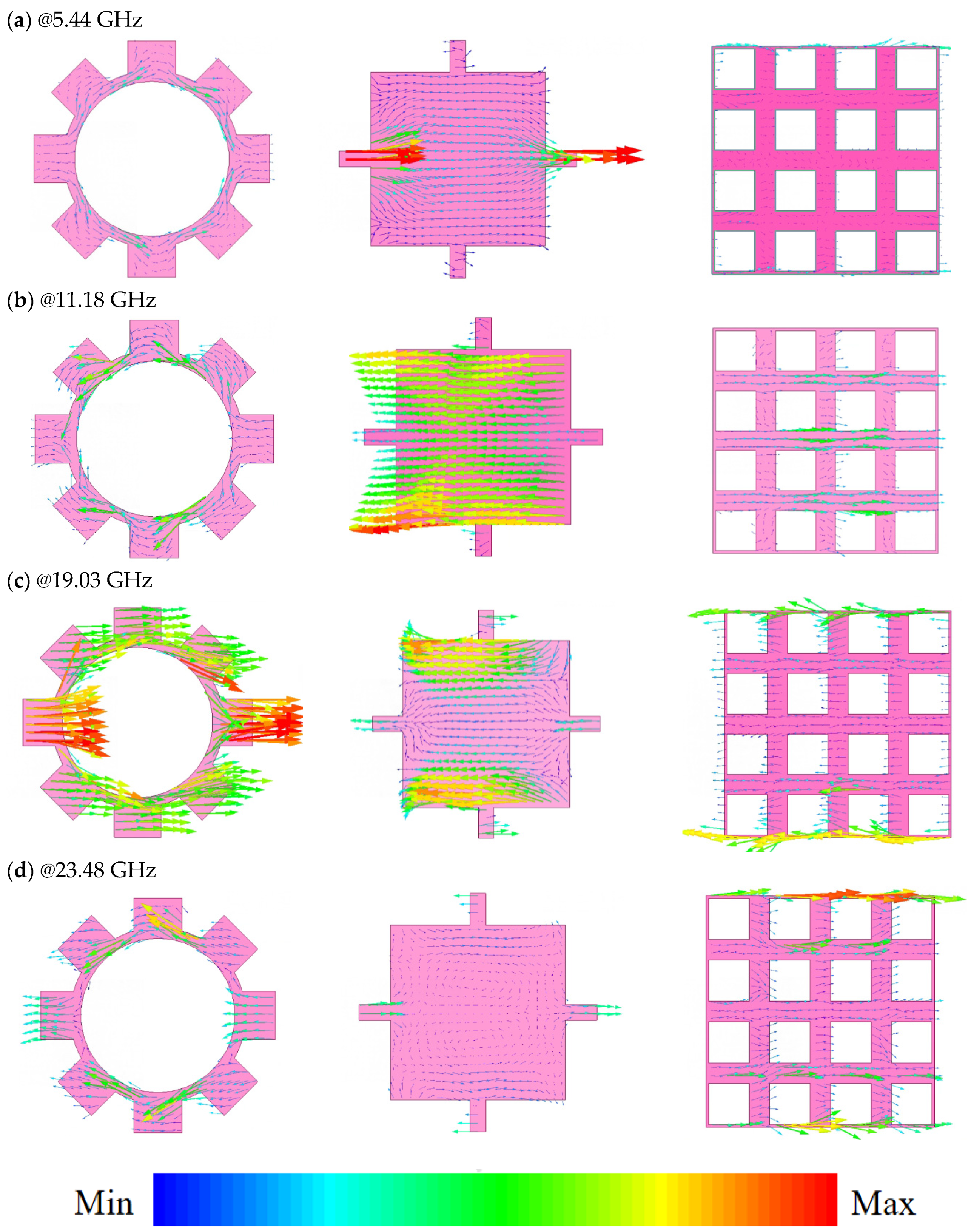
The surface current generated in the resonant structure of the absorber can visually explain the absorption mechanism of the microwave absorber. To observe the surface current distribution at the four resonant frequencies—5.44 GHz, 11.18 GHz, 19.03 GHz, and 23.48 GHz. We present the surface current distribution of the ITO resonant patterns in different layers to further explore the absorption mechanism. As shown in
Figure 8a–d, at 5.44 GHz (
Figure 8a), the surface current mainly concentrates on the middle layer’s ITO resonant pattern, with the upper layer’s current being similar, strengthening the electric resonance. The grid-like ITO back plate shows weak surface current at low frequencies. At 11.18 GHz (
Figure 8b), the surface current directions are consistent with those at 5.44 GHz, enhancing the electric resonance, while the back plate generates a reverse resonant current, forming a circulation loop akin to a magnetic dipole, further strengthening the magnetic field effect. At 19.03 GHz (
Figure 8c), the surface current mainly concentrates on the upper and middle ITO resonant patterns, with opposing current directions, forming strong internal circulation loops that enhance magnetic resonance between the patterns. The current distribution on the grid-like ITO back plate exhibits strong surface currents at both the top and bottom of the absorber structure. These currents are aligned with the surface currents on the ITO resonant patterns in the middle layer, thereby reinforcing the electric resonance between the two layers. In contrast, at 23.48 GHz (
Figure 8d), the surface current directions in the upper, middle, and lower ITO layers become disorganized, showing weak electromagnetic resonance. When electromagnetic waves are incidence normally on the ultra-wideband MA, the ITO resonant patterns generate surface currents, which convert electromagnetic waves into heat via the ITO resistive films, dissipating the energy and thus achieving absorption. This is a key mechanism behind ultra-wideband absorption.
In order to better explain the resonance mode of MAs, an equivalent circuit model (ECM) is proposed to analyze the ultrawideband absorption response based on the transmission line theory and equivalent circuit theory, as shown in
Figure 9. According to transmission line theory, a dielectric layer in free space can be equivalently represented by its characteristic impedance. Specifically, the characteristic impedance of the PMMA dielectric layer is expressed as Z
c1 = Z
0/(ε
1)
0.5, while the characteristic impedance of the PET dielectric layer is expressed as Z
c2 = Z
0/(ε
2)
0.5, ε
1 and ε
2 represent the dielectric constants of the PMMA and PET dielectric layers, respectively. From
Figure 2, it can be observed that within the operating frequency range, S
21 remains below −15 dB. This indicates that the mesh grid backplane can be regarded as a fully reflective short-circuit surface, which is represented as a resistive element R
g in the equivalent circuit. Furthermore, the analysis of
Figure 8 reveals that the ITO resonant patterned layer serves as the primary source of resonance and is the main contributor to the dissipation of the incident electromagnetic wave energy. This is a key factor in achieving ultra-broadband absorption. Based on the analysis of the absorption performance of the MA, the ITO resonant pattern can be represented as two RLC resonant circuits in
Figure 9. Based on the equivalent circuit model provided in
Figure 9, the input impedance of each RLC resonant circuit can be calculated using the following formula:
Since the ground layer can be regarded as a fully reflective short-circuit surface, the equivalent resistance R
g is zero. According to transmission line theory, Z
in3 can be expressed as:
Additionally, the input impedance can be expressed using the following equation:
Here, βi = (2πf(εi)0.5)/c, (i = 1,2) represents the propagation constant of the incident electromagnetic wave, where f is the frequency of the incident wave, and c is the speed of light. Additionally, H1 and H2 denote the thicknesses of the PMMA and PET layers, respectively. Through Equations (7)–(9), it can be observed that the absorption of a multilayer microwave absorber can be represented by a corresponding transmission line circuit. According to impedance matching theory, achieving high absorption requires the total equivalent input impedance Zin to approach Z0. Examining the input impedance Equations (8) and (9), it is evident that variations in the dielectric layer type and thickness lead to changes in the circuit parameters. By optimizing the design of the periodic ITO patterns, selecting appropriate dielectric materials, and adjusting the thickness of the dielectric layers, the input impedance of the MMA can be effectively tuned to approach Z0. This is the most critical factor enabling multilayer microwave absorbers to achieve ultra-broadband absorption capability.
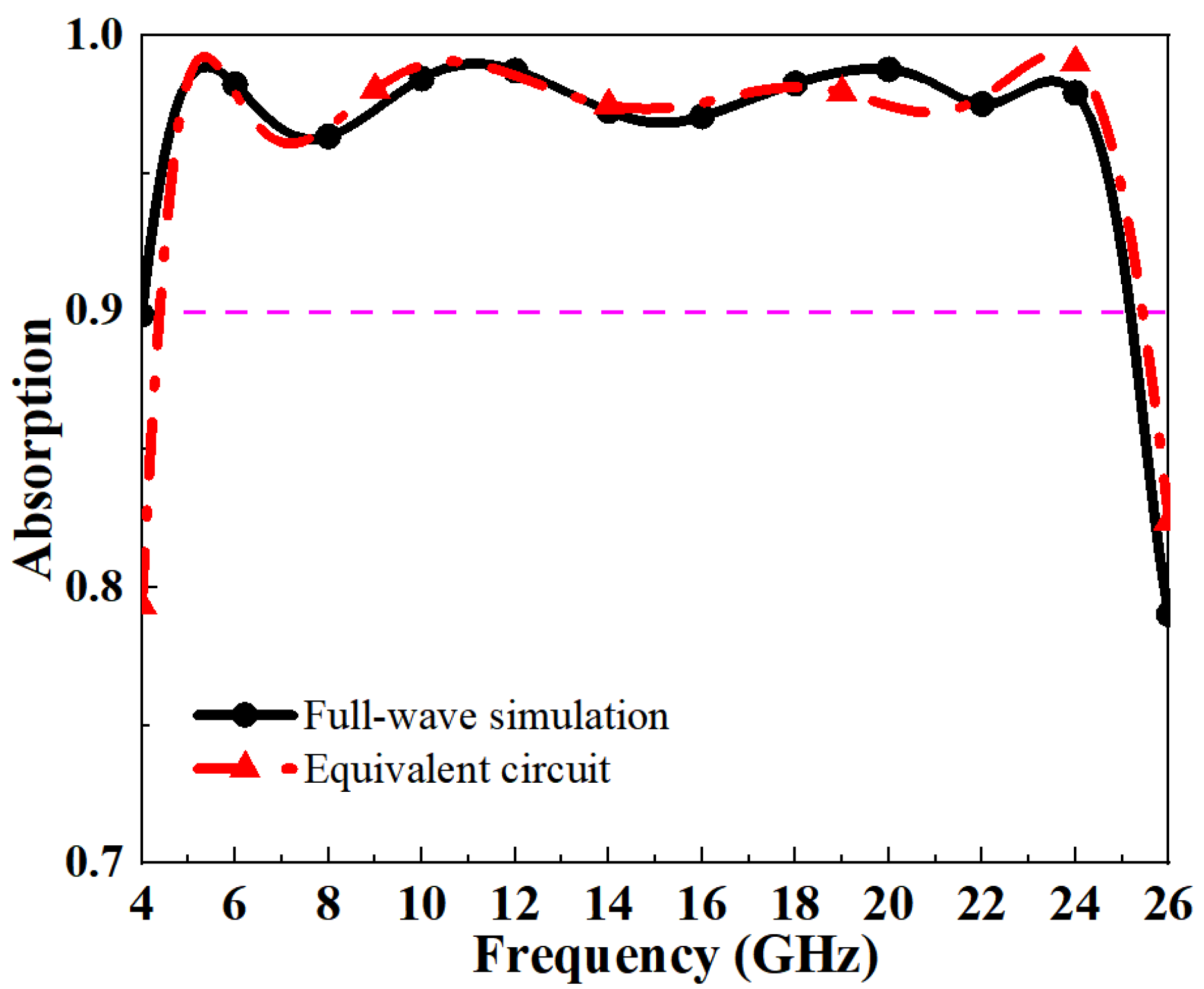
According to the above equivalent circuit model, the parameters of each lumped element are calculated and improved by ADS simulation software (2024). As shown in
Figure 10, the results of ADS simulation are basically consistent with those of full-wave simulation, which further explains the reliability of the design. The relevant lumped element parameters are as follows: R
1 = 498.64 Ω, L
1 = 2.11 nH, c
1 = 60.34 fF, R
2 = 155.71 Ω, L
2 = 1.24 nH, c
2 = 143.74 pF.
Next, through the analysis of surface currents at different absorption peaks, it can be concluded that the broadband absorption mechanism of the microwave absorber is primarily influenced by the High ohmic loss effect of the ITO resonant patterns. Furthermore, this dissipation effect can be quantified by the dissipation factor Q, which can be expressed using the following formula:
Here, f resents the resonant frequency, ∆f is the absorption bandwidth, P
t is the stored energy, and P
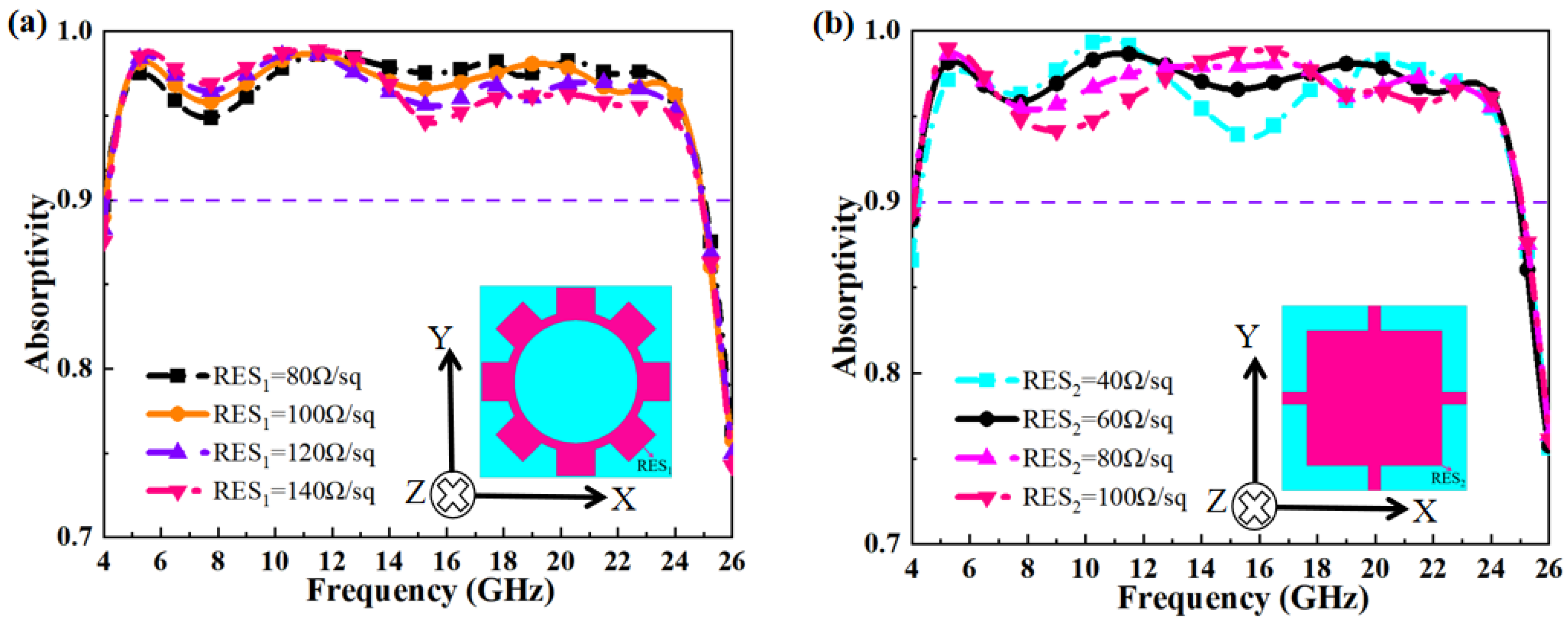
a is the dissipated energy. From Equation (10), it can be seen that the dissipated energy is directly proportional to the absorption bandwidth. Based on the surface current analysis, it is clear that the higher the dissipation effect of the ITO resonant patterns, the broader the predicted absorption bandwidth. Significant electromagnetic effects are observed in the upper and middle ITO layers, so a parametric sweep was performed, as shown in
Figure 11a,b.
From
Figure 11a, it can be observed that when RES
1 varies, the absorption rate of the MA remains relatively stable, showing only slight fluctuations. To optimize absorption performance, RES
1 is set to 100 Ω/sq in this design. The surface current analysis in
Figure 8 indicates that RES
2 plays a crucial role in the overall electromagnetic resonance, which is key to achieving ultra-wideband absorption.
Figure 11b shows that when the ITO resistance fluctuates around 60 Ω/sq, the number of absorption peaks decreases, and the second peak shifts to higher frequencies, weakening dissipation. Therefore, RES
2 is set to 60 Ω/sq to ensure optimal absorption performance.


