Article

Compact Modeling and Exploration of the Light Metal Insertion Effect for a Voltage-Controlled Spin–Orbit Torque Magnetic Tunnel Junction

by
Weixiang Li
1,2,†,
Jiaqi Lu
1,2,†,
Chengzhi Wang
1,* and
Dongsheng Wang
1,*
1
National Innovation Institute of Defense Technology, Academy of Military Sciences, Beijing 100091, China
2
Fert Beijing Institute, School of Integrated Circuit Science and Engineering, Beihang University, Beijing 100191, China
*
Authors to whom correspondence should be addressed.
These authors contributed equally to this work.
Electronics 2025, 14(7), 1272; https://doi.org/10.3390/electronics14071272
Submission received: 5 February 2025 / Revised: 18 March 2025 / Accepted: 20 March 2025 / Published: 24 March 2025

Abstract

:
Magnetic random-access memory, recognized as a breakthrough in spintronics, demonstrates substantial potential for next-generation nonvolatile memory and logic devices due to its unique magnetization-switching mechanism. However, realizing reliable perpendicular magnetization switching via spin–orbit torque necessitates an externally applied in-plane magnetic bias, a requirement that complicates integration in high-density device architectures. This study proposes a novel device architecture where geometric asymmetry engineering in an interlayer design generates an intrinsic equivalent in-plane magnetic field. By strategically introducing a non-symmetrical spacer between the heavy metal and ferromagnetic layers, we establish deterministic magnetization reversal while eliminating external field dependency. Furthermore, the energy barrier during magnetization switching is dynamically adjusted by applying a voltage across a perpendicular-anisotropy magnetic tunnel junction, leveraging the voltage-controlled magnetic anisotropy effect. We established a physics-driven compact model to assess the design and performance of voltage-controlled spin–orbit torque magnetic tunnel junction (VCSOT-MTJ) devices. Simulations reveal that the introduction of a minimally asymmetric light metal layer effectively resolves the issue of incomplete switching in field-free spin-orbit torque systems.

1. Introduction

With the continual miniaturization of technology, power dissipation has become one of the most critical issues, challenging the continuation of Moor’s law [1,2]. Emerging non-volatile technologies are highly appealing for resolving this problem. For instance, nanopillars based on magnetic tunnel junctions (MTJs) are emerging as very promising contenders for non-volatile memory and logic applications. This is due to their non-volatility, high-speed performance, low power consumption, almost limitless endurance, excellent scalability, and strong compatibility with CMOS process technology [3,4]. A major challenge in MTJ development is formulating effective magnetization-switching strategies. Traditionally, spin transfer torque (STT) has been utilized to change the magnetization of the free layer by injecting a spin-polarized current perpendicular to the film plane [5,6]. Nevertheless, at present, STT-MTJs have a significant write-delay issue because of their inherent incubation time. Additionally, the critical current for STT switching is correlated with thermal stability [7]. To prevent barrier breakdown, the write current must be kept relatively low, which leads to a long write delay [8].
To address the limitations of the STT-MTJs, spin-orbit torque (SOT) has been extensively studied due to its potential to enable faster and more energy-efficient writing in MTJs. These experimental setups employ a three-terminal configuration where a ferromagnetic heterostructure is created by depositing a heavy metal electrode on the MTJ’s free layer. This architecture leverages the synergistic action of spin–orbit coupling phenomena, through which in-plane current excitation in the heavy metal layer induces the necessary SOT for deterministic magnetization switching in the adjacent ferromagnetic layer [8,9,10]. However, achieving deterministic switching in p-MTJ devices necessitates an additional in-plane magnetic field, which is impractical for high-density magnetic random-access memory (MRAM) applications [11,12].
Fortunately, recent experiments have shown that inserting a slightly asymmetric light metal layer between the heavy metal layer and the ferromagnetic layer can achieve deterministic switching without an external magnetic field. The absence of structural symmetry along the z-axis induces the emergence of a polarized electric field (Ebi) perpendicular to the surface, thereby generating spin–orbit torque through lattice distortion mechanisms [13]. Nevertheless, the Ebi in these configurations is relatively weak, leading to incomplete field-free SOT switching and, consequently, severe switching unreliability. Moreover, the critical SOT current is still large, resulting in high power consumption [11].
One way to deal with these problems is to bring in the voltage-controlled magnetic anisotropy (VCMA) effect. When gate voltage (VG) is applied across the interface, it induces a redistribution of charges at the interface. This redistribution alters the electronic structure, particularly the occupancy of orbitals, which, in turn, affects the spin–orbit coupling and the magnetic anisotropy energy. As a result, power consumption can be cut down [14].
In this paper, we introduce the initial compact model for a three-terminal magnetic tunnel junction device with voltage-controlled spin–orbit torque (VCSOT) functionality, which has an HM/LM/FM/oxide stack. This model consists of three main parts, the circuit module, the tunnel magnetoresistance module, and the switching dynamics module, all of which are programmed in the Verilog-A language. The remaining parts of this paper are organized into three principal components: A theoretical framework for the compact VCSOT-MTJ architecture with gradient-doped light metal interlayer is systematically elaborated in Section 2, followed by the influence of the VCMA effect on SOT switching. Finally, Section 4 provides the conclusion of this work.

2. Compact Model for the VCSOT-MTJ Device

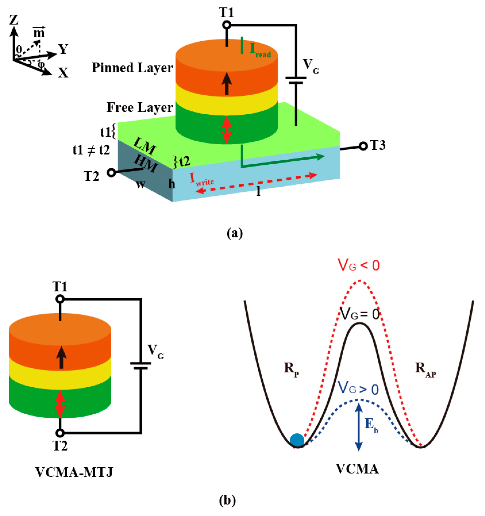
2.1. Structure of the VCSOT-MTJ

Figure 1a shows the structure of the VCSOT-MTJ device [11]. This device is made up of a p-MTJ, a slightly asymmetric light metal (LM), and a heavy metal (HM), with the LM placed between the HM and the p-MTJ [13]. p-MTJ nanopillars mainly consist of two ferromagnetic (FM) layers, like CoFeB, and a thin oxide barrier, such as MgO. In MTJs, one FM layer maintains fixed magnetization (the pinned layer), while the other FM layer exhibits switchable bistability (the free layer). Based on the relative orientation of magnetization in these two FM layers, the device operates through two distinct resistance states: parallel (P) or antiparallel (AP). Each MTJ can show two stable resistance states, RP or RAP, which are used to represent digital logic [15]. The Ti layer is deposited via inclined sputtering, achieving angular deviation using a substrate holder fixation system. This orientation preserves planar uniformity while enabling the conformal coverage of 3D nanostructures without mechanical rotation during deposition. This results in a slightly asymmetric Ti layer with different thicknesses, t1 and t2, at its ends [13]. This leads to the breaking of the mirror symmetry in relation to the yz plane. As a result, a built-in effective electric field can be generated along the x-axis. However, due to the insertion of the Ti layer and the small spin Hall angle of the heavy metal, the critical current is still high, resulting in high power consumption. To address this limitation, we introduce the VCMA effect into this model. With the help of the electric field, the p-MTJ can be switched to the AP (or P) state without the assistance of an external magnetic field. Figure 1b shows that under the VCMA effect, the energy barrier (Eb) for the reversal of the free layer in VCSOT-MTJ devices can be modulated by voltage (VG) so that the threshold current required for device reversal can be adjusted by the VG.

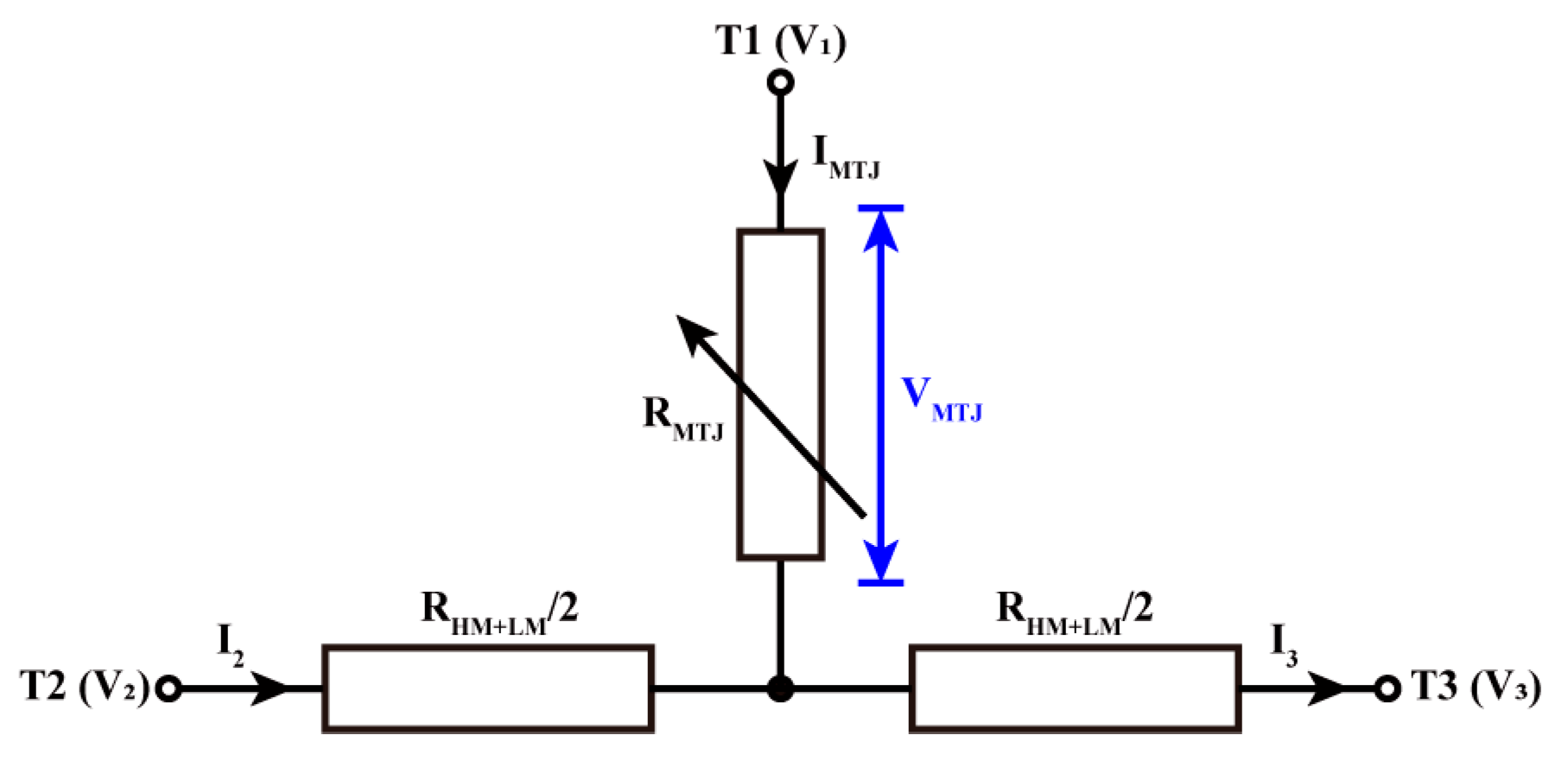
2.2. Electrical Model of the VCSOT-MTJ

The electrical characteristics of the VCSOT-MTJ device enable its representation as a T-type resistive model, as demonstrated schematically in Figure 2. In this model, the resistance of the MTJ is denoted by RMTJ, while the combined resistance of the heavy metal layer and the light metal film in parallel is represented by RHM+LM.
According to the law of resistance, we can obtain
R H M = ρ H M L H M W H M H H M
where R H M stands for the resistance, ρ H M for the resistivity, L H M for the length, W H M for the width, and H H M for the height of the heavy metal strip.
R L M = 2 L L M ( t 1 + t 2 ) W L M
where R L M , ρ H M , L L M , and W L M represent the resistance, resistivity, length, and width of the light metal film, respectively.
Using the formula for calculating parallel resistance, we can obtain Equation (3). After substituting Equations (1) and (2) into Equation (3) and then simplifying, we can derive Equation (4).
R H M + L M = R H M × R L M R H M + R L M
R H M + L M = 2 L H M L L M W L M H H M L H M W L M ( t 1 + t 2 ) + 2 L L M W H M
where R H M + L M represents the parallel resistance of the light metal film and the heavy metal bar. Based on Kirchhoff’s circuit laws, it is possible to derive
I 2 + I M T J = I 3 0.5 I 2 R H M + L M + 0.5 I 3 R H M + L M = V 2 V 3 I M T J R M T J + 0.5 I 3 R H M + L M = V 1 V 3
By rearranging Equation (5), we can derive the following result.
I M T J = 4 V 1 2 V 2 2 V 3 / 4 R M T J + R H M + L M I 2 = V 2 V 3 / R H M + L M 0.5 I M T J I 3 = V 2 V 3 / R H M + L M + 0.5 I M T J
According to Equation (6), it is known that half of the IMTJ current flows out from T2, and the other half flows out from T3, indicating that the SOT effect caused by the SHE effect of the IMTJ can cancel. This indicates that the IMTJ makes no contribution to the SOT. Consequently, the ISOT current can be computed as shown below.
I S O T = ( V 2 V 3 ) / R H M + L M

2.3. Model of Tunneling Magnetoresistance in VCSOT-MTJ

Based on the Brinkman tunneling resistance model, the resistance (RP) of the MTJ in the P state is described by [16,17].
R P = t o x F × φ ¯ 1 / 2 × A M T J × e x p ( 2 t o x ( 2 m e φ ¯ ) 1 / 2 )
RP (Parallel State Resistance) characterizes the conductive state when magnetic moments are aligned, while tox denotes the MgO barrier thickness governing quantum tunneling probability. F is a factor computed from R·A, which represents the resistance–area product. The effective barrier potential is described by φ ¯ (mean barrier height), AMTJ specifies the cross-sectional area of the MTJ, is the symbol for the reduced Planck constant, m represents the mass of the electron, and e represents the charge of the electron.
The TMR ratio is a parameter used to describe the resistance difference of the MTJ in the parallel and antiparallel states, as stated in Ref. [17], and it can be expressed by Equation (9). In order to describe the dynamic behavior of TMR [3], the voltage-dependent TMR effect is described with Equation (10).
T M R = R A P R P R P
T M R r e a l = T M R 1 + V M T J 2 / V h 2
where VMTJ is the bias voltage across the MTJ, TMRreal (VMTJ) is the actual TMR value at VMTJ, TMR stands for the maximum TMR value when the bias voltage is zero, and Vh is a characteristic voltage related to the physical properties of the MTJ device, which results in TMRreal (Vh) = 0.5 × TMR. Then, the RMTJ can be calculated using Equation (11) [8,11].
R M T J ( V M T J ) = R p [ 1 + ( V M T J / V h ) 2 + T M R ] 1 + V M T J 2 / V h 2 + T M R [ 0.5 ( 1 + c o s θ ) ]
where θ represents the angle between the magnetization directions of the free layer and the fixed layer.

2.4. Magnetization Dynamics Model of the VCSOT-MTJ

The magnetization direction in the free layer has certain dynamic behaviors, which can be depicted by an altered LLGS equation, as described in [18,19]:
d m f r e e d t = γ m f r e e × H E F F + α m f r e e × d m f r e e d t + γ τ S T T + γ τ S O T
m f r e e denotes the unit vector corresponding to the spin magnetic moment in the direction of the free layer’s magnetization; t represents time; and the gyromagnetic ratio, γ , is constant. The effective field, H E F F , incorporates both externally applied fields and intrinsic magnetostatic interactions; the damping constant, α , quantifies the energy dissipation mechanisms; τ S T T is the spin-transfer torque; and τ S O T is the spin–orbit torque. τ S T T and τ S O T both contain damping-like (DL) torques and field-like (FL) torques. DL directly affects the precession and relaxation processes of the magnetization vector, while FL torque typically affects the effective field of the magnetization vector, which may be considered a slower, more stable effect in some cases; therefore, the model does not include the FL torque term [11,19].
τ S T T = τ s t t D L m f r e e × m p × m f r e e + τ s t t F L m f r e e × m p
τ S O T = τ s o t D L m f r e e × m σ × m f r e e + τ s o t F L m f r e e × m σ
τ s t t D L = P J s t t 2 e μ 0 M s t f l
τ s o t D L = θ J s o t 2 e μ 0 M s t f l
The reference layer’s magnetization configuration is mathematically represented by the vector field, m p , while the emergent electron polarization component, m σ , arises from spin–orbit coupling phenomena. is the reduced Planck constant, P is the spin polarization, J s t t is the spin-polarized current density through the MTJ, e is the elementary charge, μ 0 is the vacuum permeability, M s is the saturation magnetization, and t f l is the thickness of the FL. The thickness of the film can affect the magnetic properties of the material. J s o t is the current density injected into the HM layer, and θ is the effective spin Hall angle, which influences spin transport efficiency through the material’s intrinsic properties.

2.5. Effective Magnetic Field

For the VCSOT-MTJ with a hybrid multilayer structure [HM/LM/FM/oxide], the effective magnetic field, H E F F , emerges from multiple interrelated components.
H E F F = H H M + L M + H P M A + H V C M A + H D + H T H
where H H M + L M is a current-induced perpendicular magnetic field created by the broken symmetry [13]. H P M A represents the magnetic field due to PMA. H V C M A describes the magnetic field due to the VCMA effect in the MTJ. H D describes the demagnetizing field. H T H is the thermal magnetic field, which represents the random fluctuations in the magnetic field due to thermal energy. When the thickness of the light metal layer, Ti, is 0.58 nm, the relationship between H H M + L M and the current density is as follows [13]:
H H M + L M = ( 4.82527 ) J W 0.0096 m z
where J W is the current density flowing through the heavy metal layer. The direction of H H M + L M depends on the polarity of the applied current. For a positive current (applied in the +y-direction), H H M + L M points toward +z. For a negative current (applied in the −y-direction), H H M + L M points toward −z.
H P M A = 2 K i t f l μ 0 M s m z
where K i is the perpendicular magnetic anisotropy constant, a material parameter that indicates the difference in magnetic energy between the perpendicular direction and the easy magnetization direction. In thin film magnetic materials, the thickness can affect the magnetic properties. m z is the unit magnetization vector along the z-axis. It indicates the degree of magnetization of the material along the z-axis.
H V C M A = 2 ξ V M T J t f l μ 0 M s t M g O m z
where ξ is a proportionality constant that relates the current-induced torque to the magnetic anisotropy. VMTJ is the volume of the magnetic tunnel junction, which can influence the strength of the VCMA effect. tMgO is the thickness of the MgO barrier in the MTJ, which can significantly affect tunneling magnetoresistance and the VCMA effect. m z is the unit magnetization vector along the z-axis, indicating the direction of magnetization.
H D = M s ( N · m )
N x = N y = π t f / ( 4 D ) N z = 1 2 · N x = 1 2 π t f / ( 4 D )
where N is the demagnetizing factor, a tensor that describes how the magnetization of a material affects the internal magnetic field. m is the magnetization moment of the material. N z is the component of the demagnetizing factor in the z-direction. D is the characteristic length of the material.
H t h = σ 2 k B T α μ 0 M S γ V t
where σ represents the spin or the unit vector in the direction of magnetization. k B is the Boltzmann constant, which relates the temperature of a system to its thermal energy. T is the temperature in Kelvin. α is the Gilbert damping parameter, which characterizes the damping of magnetic precession and is associated with the dissipation of energy in magnetic systems. M S is the saturation magnetization, which is the maximum magnetization that a material can achieve. γ is the gyromagnetic ratio, which relates the magnetic moment of a particle to its angular momentum. V is the volume of the material. t is the time increment, which is relevant in the context of dynamic simulations or time-dependent processes. In the Cartesian coordinate system, the x-, y-, and z-axis components of the effective magnetic field, H E F F , can be decomposed as follows [11]:
H E F F X = H D X + σ x 2 k B T α u 0 M S γ V t   H E F F Y = H D Y + σ y 2 k B T α u 0 M S γ V t H E F F Z = H E F F + H D Z + σ z 2 k B T α u 0 M S γ V t H E F F = ( 4.82527 J W 0.0096 + 2 K i μ 0 M s t f 2 β V M T J μ 0 M s t o x t f N z z M S ) m Z
θ t = γ 1 + α 2 [ H E F F X ( α c o s θ c o s φ s i n φ ) + H E F F Y ( α c o s θ s i n φ + c o s φ ) α H E F F Z s i n θ ] + γ s i n θ 1 + α 2 ( α H S T T F L H S T T D L ) γ H S O T D L 1 + α 2 ( α s i n φ + c o s θ c o s φ ) + γ H S O T F L 1 + α 2 ( α cos θ cos φ sin φ ) φ t = γ ( 1 + α 2 ) s i n θ [ H E F F X ( α s i n φ c o s θ c o s φ ) + H E F F Y ( α c o s φ c o s θ s i n φ ) + H E F F Z s i n θ ] γ 1 + α 2 ( α H S T T D L + H S T T F L ) γ H S O T D L ( 1 + α 2 ) s i n θ ( α c o s θ c o s φ s i n φ ) γ H S O T F L ( 1 + α 2 ) s i n θ ( α sin φ cos θ c o s φ )
where we assume that m = s i n θ c o s φ e x + s i n θ s i n φ e y + c o s θ e z , m p = ( 0,0 , 1 ) , and m σ = ( 1,0 , 0 ) .

3. Electrical Compact Model and Simulations

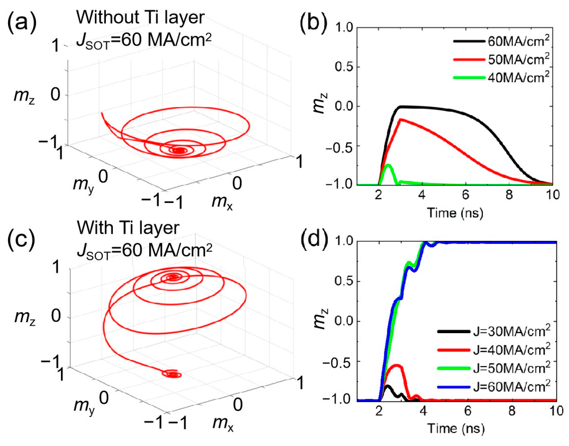
3.1. Field-Free SOT Switching Without VCMA Effect

In this section, we investigate SOT-driven magnetization switching by incorporating an asymmetric Ti layer. Due to the large resistance of the magnetic tunnel junction (RMTJ) resulting from the thick oxide layer (tox), the tunneling current through the MTJ (IMTJ) is significantly reduced. Consequently, the contribution of STT induced by the IMTJ is negligible during the switching process. Therefore, in the following analysis of the VCSOT-MTJ device, the influence of STT is disregarded.
Particularly, a higher Ms increases the energy barrier for switching, leading to higher critical current densities, while a lower MS reduces the energy barrier, improving energy efficiency but potentially compromising thermal stability. Variations in R·A impact the TMR ratio and switching dynamics, with higher R·A values generally resulting in slower switching speeds but higher signal integrity. The spin Hall angle and resistivity influence the magnetic field distribution and spin current generation, affecting the overall efficiency of the SOT switching process.
Therefore, we conducted the simulation by using the parameters in Table 1. Figure 3a depicts the dynamic switching behavior of a three-terminal MTJ without an asymmetric Ti layer under a SOT current density of JSOT = 50 MA/cm2. The initial magnetization state (mz) is along the −z-axis (mz = −1). Upon applying the SOT current, the magnetization is initially driven toward an in-plane orientation due to the torque-induced dynamics. However, the magnetization subsequently relaxes back to its original state, dominated by demagnetization energy. This results in an incomplete and non-deterministic switching process.
Figure 3b presents the time-resolved evolution of mz for different SOT current densities (JSOT = 40, 50, and 60 MA/cm2). The SOT current is applied at t = 2 ns with a pulse duration of 1 ns. As the current density increases, mz rises more rapidly, reaching a transient in-plane configuration. Nevertheless, even at the highest current density, JSOT = 60 MA/cm2, the SOT fails to achieve complete magnetization switching, highlighting the limitations of the structure without additional symmetry-breaking layers.
To address this, a thin asymmetry Ti layer was introduced into the MTJ structure, as suggested by Ref. [13]. Figure 3c shows how the modified MTJ with the Ti layer dynamically switches when subjected to a JSOT of 50 MA/cm2. The insertion of the Ti layer enables deterministic, field-free SOT switching, overcoming the limitations observed in the original structure. The aid of the Ti layer induces sufficient asymmetry to facilitate robust switching. Although structure symmetry breaking has been explored in previous works [20,21,22], its fabrication and application remain challenging. Techniques relying on the antiferromagnetic spin Hall effect are constrained by materials with small spin Hall angles, which inherently limit their efficiency and performance. Methods utilizing PMN-PT materials encounter substantial fabrication challenges due to their complex structural requirements. Approaches combining SOT and STT are prone to device breakdown risks caused by the high current densities required for operation. Compared with the above field-free methods, this method of field-free switching maintains a straightforward fabrication process.
Figure 3d compares the time evolution of mz for varying SOT current densities (JSOT = 30, 40, 50, and 60 MA/cm2) in the presence of the Ti layer. Deterministic switching is achieved at JSOT ≥ 50 MA/cm2; the switching process fails, indicating a critical current density for successful magnetization reversal. Although the Ti layer significantly improves switching performance, the relatively weak asymmetry still results in a high critical switching current, contributing to substantial energy consumption.

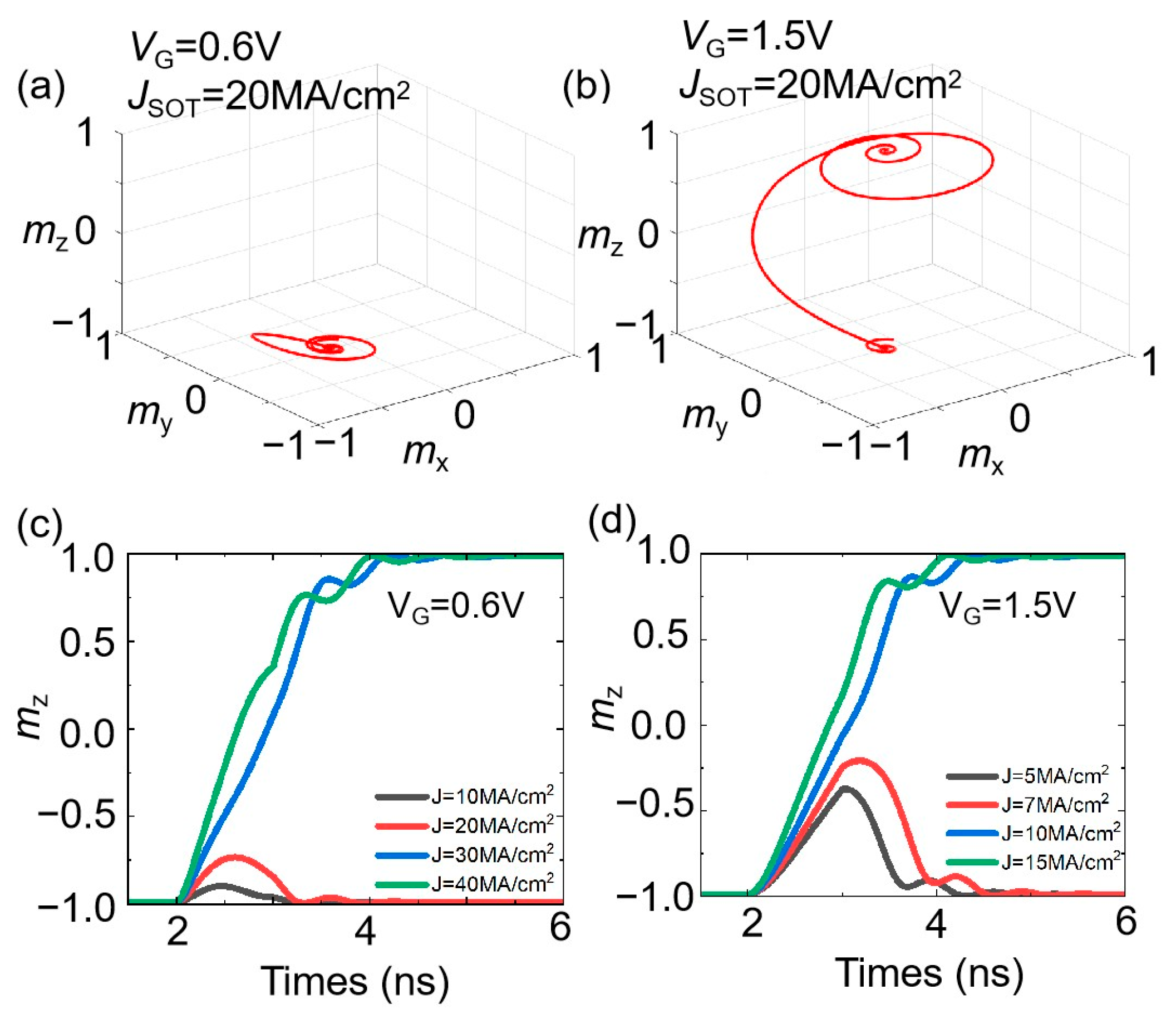
3.2. DC Simulation of the VCSOT-MTJ

To reduce power consumption in the SOT switching model, the VCMA effect was introduced into the model. Figure 4a,b demonstrate the impact of voltage (VG) on magnetization dynamics under a constant SOT current density of JSOT = 20 MA/cm2 (Figure 4a); the applied SOT current fails to switch the magnetization completely under 0.6 V, with the magnetization remaining near its initial configuration. However, as VG increases to 1.5 V (Figure 4b), the enhanced VCMA effect successfully assists the SOT in switching the free layer magnetization, demonstrating the synergistic effect of the electric field on SOT-driven magnetization switching. Figure 4c,d further explore voltage-controlled SOT-driven magnetization switching under different SOT current densities (JSOT) for VG = 0.6 V and VG = 1.5 V, respectively. At VG = 0.6 V (Figure 4c), there are higher SOT current densities.
Specifically, the VCMA effect alters the interfacial magnetic anisotropy, reducing the energy barrier for magnetization switching. By lowering the critical current density required for switching, the VCMA effect significantly reduces power consumption in the SOT switching process. The simulations of the VCSOT-MTJ show the great potential for designing energy-efficient spintronic devices.

4. Conclusions

In this paper, we developed a compact model based on physics for a three-terminal VCSOT-MTJ device, aimed at a next-generation MRAM design. The simulation results demonstrate that the incorporation of an asymmetric Ti layer between the heavy metal and ferromagnetic layers enables field-free SOT switching. The integration of the VCMA effect further substantially cuts down the critical current, thus decreasing the power consumption during writing. The proposed VCSOT-MTJ device, enhanced with an asymmetric Ti layer, shows great potential for advancing energy-efficient and scalable MRAM technology for future applications.

Author Contributions

Conceptualization, W.L.; Resources, J.L.; Data curation, D.W.; Funding acquisition, C.W. All authors have read and agreed to the published version of the manuscript.

Funding

This research was funded by the National Natural Science Foundation of China under Grant 62104259.

Data Availability Statement

Data are contained within the article.

Conflicts of Interest

The authors declare no conflict of interest.

References

  1. Swami, S.; Mohanram, K. Reliable nonvolatile memories: Techniques and measures. IEEE Des. Test 2017, 34, 31–41. [Google Scholar] [CrossRef]
  2. Xia, Y.; Zhang, K.; Zeng, L.; Zhang, Y.; Zhao, W.; Zhang, D. A Novel Non-Voltatile Magnetic Majority Gate with Voltage-Gated Spin-Orbit Torque Magnetic Tunnel Junction Cascaded in Series for Low Power and High Reliability. IEEE-NANO 2023, 2023, 661–665. [Google Scholar] [CrossRef]
  3. Kang, W.; Ran, Y.; Zhang, Y.; Lv, W.; Zhao, W. Modeling and exploration of the voltage-controlled magnetic anisotropy effect for the next-generation low-power and high-speed MRAM applications. IEEE Trans. Nanotechnol. 2017, 16, 387–395. [Google Scholar] [CrossRef]
  4. Halawani, Y. Impact of Emerging Memory Technologies on the Energy Efficiency of Wireless Sensor Nodes. Ph.D. Thesis, Khalifa University, Abu Dhabi, United Arab Emirates, 2014. [Google Scholar]
  5. Apalkov, D.; Khvalkovskiy, A.; Watts, S.; Nikitin, V.; Tang, X.; Lottis, D.; Moon, K.; Luo, X.; Chen, E.; Ong, A.; et al. Spin-transfer torque magnetic random access memory (STT-MRAM). JETC 2013, 9, 1–35. [Google Scholar] [CrossRef]
  6. Halawani, Y.; Mohammad, B.; Al-Qutayri, M.; Saleh, H. Modeling of STT-MTJ for low power embedded memory applications: A comparative review. In Proceedings of the 2013 IEEE 20th International Conference on Electronics, Circuits, and Systems (ICECS), Abu Dhabi, United Arab Emirates, 8–11 December 2013; pp. 719–722. [Google Scholar] [CrossRef]
  7. Kang, W.; Lv, W.; Zhang, Y.; Zhao, W. Low store power high-speed high-density nonvolatile SRAM design with spin Hall effect-driven magnetic tunnel junctions. IEEE Trans. Nanotechnol. 2016, 16, 148–154. [Google Scholar] [CrossRef]
  8. Wang, Z.; Zhao, W.; Deng, E.; Klein, J.O.; Chappert, C. Perpendicular-anisotropy magnetic tunnel junction switched by spin-Hall-assisted spin-transfer torque. J. Phys. D Appl. Phys. 2015, 48, 065001. [Google Scholar] [CrossRef]
  9. Wang, C.; Zhang, D.; Zhang, K.; Zeng, L.; Wang, Y.; Hou, Z.; Zhang, Y.; Zhao, W. Magnetic nonvolatile SRAM based on voltage-gated spin-orbit-torque magnetic tunnel junctions. IEEE Trans. Electron. Devices 2020, 67, 1965–1971. [Google Scholar] [CrossRef]
  10. Salehi, S.; Mashhadi, M.B.; Zaeemzadeh, A.; Rahnavard, N.; DeMara, R.F. Energy-aware adaptive rate and resolution sampling of spectrally sparse signals leveraging VCMA-MTJ devices. IEEE J. Emerg. Sel. Top. Circuits Syst. 2018, 8, 679–692. [Google Scholar] [CrossRef]
  11. Zhang, K.; Zhang, D.; Wang, C.; Zeng, L.; Wang, Y.; Zhao, W. Compact modeling and analysis of voltage-gated spin-orbit torque magnetic tunnel junction. IEEE Access 2020, 8, 50792–50800. [Google Scholar] [CrossRef]
  12. Li, Y.; Edmonds, K.W.; Liu, X.; Zheng, H.; Wang, K. Manipulation of magnetization by spin–orbit torque. Adv. Quantum Technol. 2019, 2, 1800052. [Google Scholar] [CrossRef]
  13. Razavi, A.; Wu, H.; Shao, Q.; Fang, C.; Dai, B.; Wong, K.; Hang, X.; Yu, G.; Wang, K.L. Deterministic spin–orbit torque switching by a light-metal insertion. Nano Lett. 2020, 20, 3703–3709. [Google Scholar] [CrossRef] [PubMed]
  14. Li, W.; Liu, Z.; Peng, S.; Lu, J.; Liu, J.; Li, X.; Lu, S.; Otani, Y.; Zhao, W. Selective Data Writing in IrMn-Based Perpendicular Magnetic Tunnel Junction Array Through Voltage-Gated Spin-Orbit Torque. IEEE Electron Device Lett. 2024, 45, 921–924. [Google Scholar] [CrossRef]
  15. Wan, Q.; Shi, Y. Neuromorphic Devices for Brain-inspired Computing: Artificial Intelligence, Perception, and Robotics; John Wiley & Sons: Hoboken, NJ, USA, 2022. [Google Scholar]
  16. Brinkman, W.F.; Dynes, R.C.; Rowell, J.M. Tunneling conductance of asymmetrical barriers. J. Appl. Phys. 1970, 41, 1915–1921. [Google Scholar] [CrossRef]
  17. Zhang, Y.; Zhao, W.; Lakys, Y.; Klein, J.O.; Kim, J.V.; Ravalosona, D.; Chappert, C. Compact modeling of perpendicular-anisotropy CoFeB/MgO magnetic tunnel junctions. IEEE Trans. Nanotechnol. 2012, 59, 819–826. [Google Scholar] [CrossRef]
  18. Pathak, S.; Youm, C.; Hong, J. Impact of spin-orbit torque on spin-transfer torque switching in magnetic tunnel junctions. Sci. Rep. 2020, 10, 2799. [Google Scholar] [CrossRef] [PubMed]
  19. Li, S.; Jiang, Y. Field-free switching model of spin–orbit torque (SOT)-MTJ device with thermal effect based on voltage-controlled magnetic anisotropy (VCMA). AIP Adv. 2023, 13, 025030. [Google Scholar] [CrossRef]
  20. Oh, Y.W.; Chris Baek, S.; Kim, Y.M.; Lee, K.D.; Yang, G.G.; Park, E.S.; Lee, K.S.; Kim, K.W.; Go, G. Field-Free Switching of perpendicular magnetization through spin-orbit torque in antiferromagnet/ferromagnet/oxide structures. Nat. Nanotechnol. 2016, 11, 878–884. [Google Scholar] [CrossRef] [PubMed]
  21. Fina, I.; Quintana, A.; Marti, X.; Sanchez, F.; Foerster, M.; Aballe, L.; Sort, J.; Fontcuberta, J. Reversible and magnetically unassisted voltage-driven switching of magnetization in FeRh/PMN-PT. Appl. Phys. Lett. 2018, 113, 152901. [Google Scholar] [CrossRef]
  22. Zhang, C.; Takeuchi, Y.; Fukami, S.; Ohno, H. Field-free and sub-ns magnetization switching of magnetic tunnel junctions by combining spin-transfer torque and spin orbit torque. Appl. Phys. Lett. 2021, 118, 092406. [Google Scholar] [CrossRef]
Figure 1. (a) Illustration of the three-terminal VCSOT-MTJ device featuring a p-MTJ/light metal/heavy metal structure. (b) VCMA mechanism: the Eb decreases as the applied gate voltage (VG) increases and increases as VG decreases.
Electronics 14 01272 g001
Figure 2. The equivalent resistance model of the VCSOT-MTJ device.
Electronics 14 01272 g002
Figure 3. (a,c) The dynamic switching characteristics of a three-terminal MTJ (a) without a Ti layer and (c) with a Ti layer under a SOT current density of JSOT = 50 MA/cm2. (b,d) The time-resolved evolution of mz in a three-terminal MTJ (b) without a Ti layer and (d) with a Ti layer for different SOT current densities.
Electronics 14 01272 g003
Figure 4. The dynamic switching behavior under a SOT current density of JSOT = 20 MA/cm2 at (a) 0.6 V and (b) 1.5 V. The time-resolved evolution of mz in a three-terminal MTJ for different SOT current densities at (c) 0.6 V and (d) 1.5 V.
Electronics 14 01272 g004
Table 1. Essential parameters for simulating VCSOT-MTJ.
ParameterDescriptionDefault Value
DDiameter of MTJ50 nm
AMTJSurface area of MTJπ × D2/4
tfFree layer height1.1 nm
toxOxide layer thickness1.4 nm
MsSaturation magnetization6.25 × 105 A/m
Ki(0)Interfacial PMA at 0 V3.2 × 10−4 J/m2
αGilbert damping factor0.05
PSpin polarization0.58
R·AResistance–area product650 Ω·µm2
TMR(0)TMR at 0 V100%
βVCMA coefficient110 fJ/V·m
LIrMnIrMn length60 nm
TIrMnIrMn thickness3 nm
ρ W Resistivity5.48 × 10−8 Ω·m
ρ T i Resistivity42 × 10−8 Ω·m
θ S H Spin Hall angle0.25
R a t i o D L F L Ratio between H S O T F L and H S O T D L 0.8
γGyromagnetic ratio2.2127 × 105 m/(A·s)
μ 0 Vacuum permeability1.2566 × 10−6 H/m
Disclaimer/Publisher’s Note: The statements, opinions and data contained in all publications are solely those of the individual author(s) and contributor(s) and not of MDPI and/or the editor(s). MDPI and/or the editor(s) disclaim responsibility for any injury to people or property resulting from any ideas, methods, instructions or products referred to in the content.

