1. Introduction
In modern scientific and industrial advancements, Time-to-Digital Converters (TDC) are a fundamental components in time-resolved systems, where the information is encoded on the basis of the occurrence time of events [
1,
2]. Owing to recent progress in performance (i.e., precision, rate, and resource consumption), TDCs gained increasing significance in a wide array of fields. Notable applications include time-resolved spectroscopy [
3,
4] and Time-Correlated Single Photon Counting (TCSPC) [
5], where timestamps are used to measure particle decay times for the extraction of key material properties. Time-of-Flight (ToF) imaging [
6,
7], including LIDAR [
8], and ToF Positron Emission Tomography (ToF-PET) [
9,
10] demonstrate further the wide spectrum of fields in which TDC use is now consolidated.
In this context, Field-Programmable Gate Arrays (FPGAs) prove to be very suited hosts for TDC implementations. In fact, they are perfect for rapid prototyping in research and development applications because of their special reconfigurability characteristic, which enables speedy adaptability to the changing demands of diverse research and industrial disciplines. FPGAs significantly reduce time-to-market, enabling rapid product development and responsiveness to market shifts and consumer preferences. Additionally, they help in cutting down nonrecurring engineering costs, providing a cost-effective alternative to custom integrated circuit solutions.
As a result, FPGAs have become consolidated tools for implementing TDC architectures [
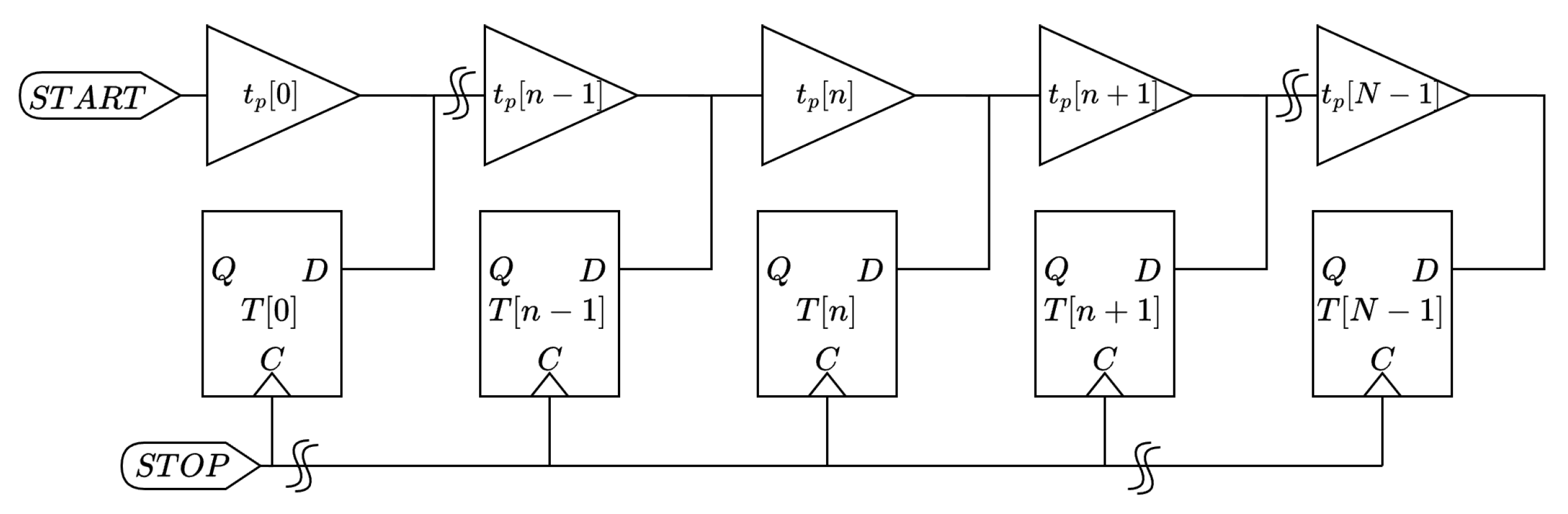
11]. In particular, the most promising one, which offers the best compromise in terms of trade-off between figures of merit precision, rate, and resource consumption, is the Tapped Delay-Line TDC (TDL-TDC) consisting of series of
N buffers (a.k.a., taps) connected in series where each buffer output is sampled by a D-type flip-flop (FF), allowing, ideally, for a simple counting mechanism on the thermometric code at the output of the FFs, to extract the delay between the signal injected in the TDL (i.e., START) and the clock of the FFs (i.e., STOP). This architecture is shown in
Figure 1.
Ideally, assuming that each buffer has the same propagation delay
and that the output of the FFs is correct (i.e., no errors introduced by skews, jitters, meta-stability, and setup and hold violations), a conversion circuit (a.k.a., decoder or encoder) can extract the number of ones
n in the
N-bit thermometric code. Under these assumptions, the time difference
between the start (
) and stop (
) events can then be computed as
Referring to Equation (
1), it is evident that the resolution (LSB) of the TDL-TDC is
, while the Full-Scale Range (FSR) is
. The digitization process introduces a quantization error (i.e.,
) uniformly distributed between
and
, with a variance of
(i.e.,
) [
12,
13]. Consequently, in the presence of jitter (i.e.,
) between the START and STOP signals caused by electronic system noise, the precision (i.e.,
) of the measured time interval (i.e.,
is impacted [
14].
However, the situation in the actual world is somewhat different, particularly when FPGAs are involved. First of all,
is not constant across the TDL due to process, voltage, and temperature (PVT) fluctuations and tolerances among devices, which make mandatory a real-time calibration process [
15,
16,
17] for estimating the propagation delay distribution through a Code Density Test (CDT) [
11]. In this way a Calibration Table (CT) is built where each tap
is characterized by its own
. The CT integration generates a Characteristic Curve (CC), which links each output code
(i.e., the number of ones in the thermometric code) to a specific timestamp
(i.e.,
with
). While it surely adds overhead, this approach correctly accounts and compensates all non-linearities affecting delay values; so, the time measurement will no longer be performed as described in Equation (
1) but rather by indexing the CC,
Under these conditions, the resolution (i.e., LSB) is better represented by the distribution of the CT and roughly by the average propagation delay
(i.e.,
) and the precision by the so-called Equivalent LSB (
) [
13], for which the mathematical expression is expressed in Equation (
4). Thus, due to the propagation delay distortion, the the quantization error is proportional to the
(i.e.,
), not to the resolution (i.e.,
)
Under these conditions, the resolution (i.e., LSB) is better characterized by the distribution of the CT and approximately by the average propagation delay (i.e.,
), while the precision is defined by the so-called Equivalent LSB (
) [
13], whose mathematical expression is provided in Equation (
4). Consequently, due to distortions in propagation delays, the quantization error is proportional to
(i.e.,
) rather than the resolution (i.e.,
).
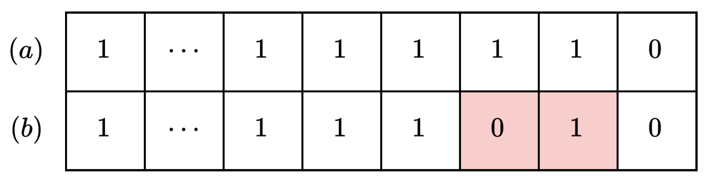
The second concern is the correctness of the thermometric code, which will be influenced by Bubble Errors (BEs) [
18], which are defined as spurious zeros in the TDL output and will be the focus of this study. An example of BE-affected code is represented in
Figure 2.
BEs arise from deterministic non-linearities in TDL propagation (e.g., skews) [
19] or from stochastic processes (e.g., sampling errors caused by setup and hold time violations) [
19]. The presence of BEs significantly affects the performance of the thermometer-to-binary converter, reducing resolution, precision, and linearity. Moreover, the behavior of the pure binary output is also influenced by the decoder architecture. It is important to mention how the decoder technique employed heavily affects the BE relevance. This is evident comparing a “sum1s” decoder [
16,
20], which counts the number of ones in the thermometric code and results in a “bubble compression”, and a “transition-based” decoder, also known as “Log2” [
11] or “one-hot” [
21], which looks for the last transition from 1 to 0 and stretches the code up to the BEs [
11,
22]. In this regard, if we consider the two codes without (a) and with (b) BEs in
Figure 2, and assuming we have an 8-tap TDL-TDC, we will obtain 7 for “11111110” and 6 for “11111010” using the sum1s decoder but the two cases will result in 7 using a “transition-based” decoder.
Discriminating between deterministic and stochastic causes of BEs is essential [
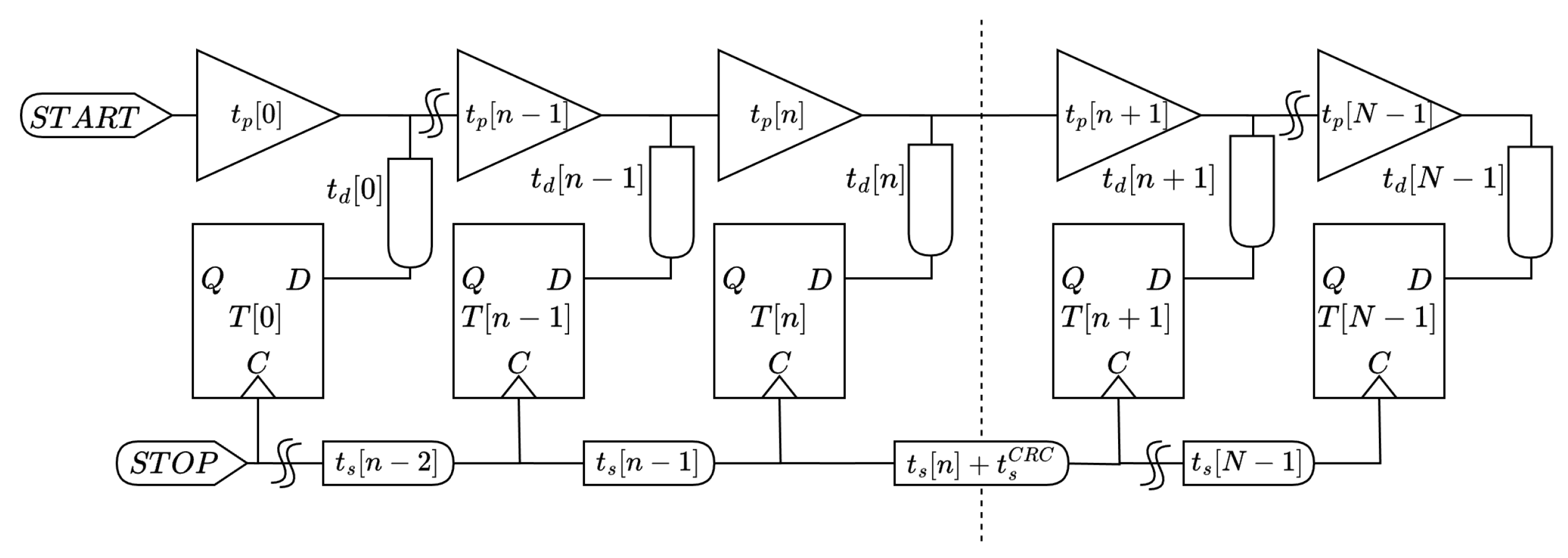
18]. Deterministic factors primarily stem from routing mismatches (
Figure 3) in particular skews (i.e.,
and
) on the clock line (i.e., STOP signal) and routing delays (i.e.,
) between buffer outputs and corresponding FF inputs [
23]. Clock skew, defined as the variation in clock arrival times at different components, also significantly contributes to BEs [
15]. Although FPGA clock networks are designed to minimize skew through hierarchical distribution in the clock regions (i.e.,
), non-negligible skew, up to tens/hundreds of picoseconds, may still arise when multiple clock regions are involved, through Clock Region Crossing (CRC), (i.e.,
). This can affect the generation of the thermometric code. If the skew and routing delays are minor compared to the buffer propagation delay
, their impact is negligible, and BEs do not occur. However, when
is shorter than these delays, the switching order of outputs may change, introducing BEs in the thermometric code and causing decoder failures. In contrast to deterministic causes, stochastic BEs arise from metastability in FFs due to violations of timing parameters (setup and hold times). This occurs when the asynchronous TDL signal is sampled improperly, causing FFs to enter a metastable state [
24]. In such cases, outputs resolve randomly as 0 or 1, unpredictably introducing BEs into the thermometric sequence.
Let us consider the TDL-TDC in
Figure 3. What needs to happen in order to prevent BEs at the position
k is as follows:
Said another way, (
5) entails that as long as the clock skew is sufficiently small or the propagation delay is suitably large, the occurrence of BEs can be completely mitigated.
TDL-TDCs offer good precision and resolution; they face a trade-off between FSR and area utilization (i.e., to double the FSR a double in area is mandatory) [
25]. This limitation is particularly pronounced in modern technological nodes (e.g., 28 nm and below), where tap propagation delays are on the order of a few picoseconds. A common approach to overcoming this trade-off is to use Nutt Interpolation [
26]. As illustrated in
Figure 4, this technique divides the measurement for all channels (e.g., START and STOP) into two components: a coarse measurement performed by an
-bit coarse counter clocked at
, and a fine measurement carried out by a TDL-TDC (i.e.,
for the START and
for the STOP). Since the START signal may occur asynchronously with the system clock, the measured time in this configuration is given by
In this way, if the dynamic range of the TDL exceeds , the FSR of the integral system is extended up to .
To enhance the resolution of TDL-TDCs beyond what is offered by the average propagation delay of the FPGA technology node (
), various sub-interpolation methods [
27,
28,
29] have been explored in the literature. These methods either involve conducting measurements across multiple parallel TDLs (
) [
30] (known as spatial sub-interpolation) or repeating measurements several times
) on the same TDL using feedback (referred to as temporal sub-interpolation) [
31], thereby creating a Virtual-TDL (VTDL) with quicker propagation delays that improve resolution. A VTDL with an
sub-interpolation order can improve, ideally, both the
and the
by a factor
, though it also increases jitter (
) compared to TDLs without sub-interpolation [
28]. One prominent example of sub-interpolation is the Wave Union A (WUA) technique. In WUA, generally two [
32] edges are sent through the same TDL for each event; a special decoder identifies the position of the two edges on the TDL, thus obtaining two real taps that are then summed to form the so-called virtual tap. The calibration algorithm will then work on the virtual tap to calculate the timestamp. In this way, the
and the
computed using the virtual tap of the VTDL are halved with respect to the real one coming from the TDL.
The aim of this paper is to detect, classify, and characterize BE artifacts using the clock signal skew on the CRC (i.e.,
) in the 28 nm Xilinx 7-Series FPGA as a case study. This is to demonstrate mathematically and verify experimentally that the presence of BEs, if properly managed, allows for a reduction in quantization error provided by the TDL-TDC. In
Section 2, we present our TDL-TDC, while in
Section 3 we address the issue and provide a model for skew-generated BEs. In
Section 4, a straightforward approach to suppress CRC skew-generated BEs is presented and analyzed. Experimental validation is reported in
Section 5. Finally,
Section 6 reports an overview about the current state of the art in terms of BE correction.
2. FPGA-Based TDL-TDC Architecture
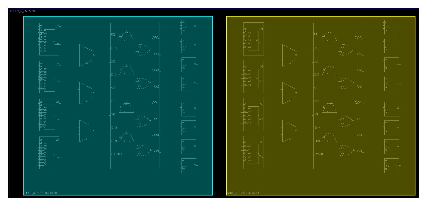
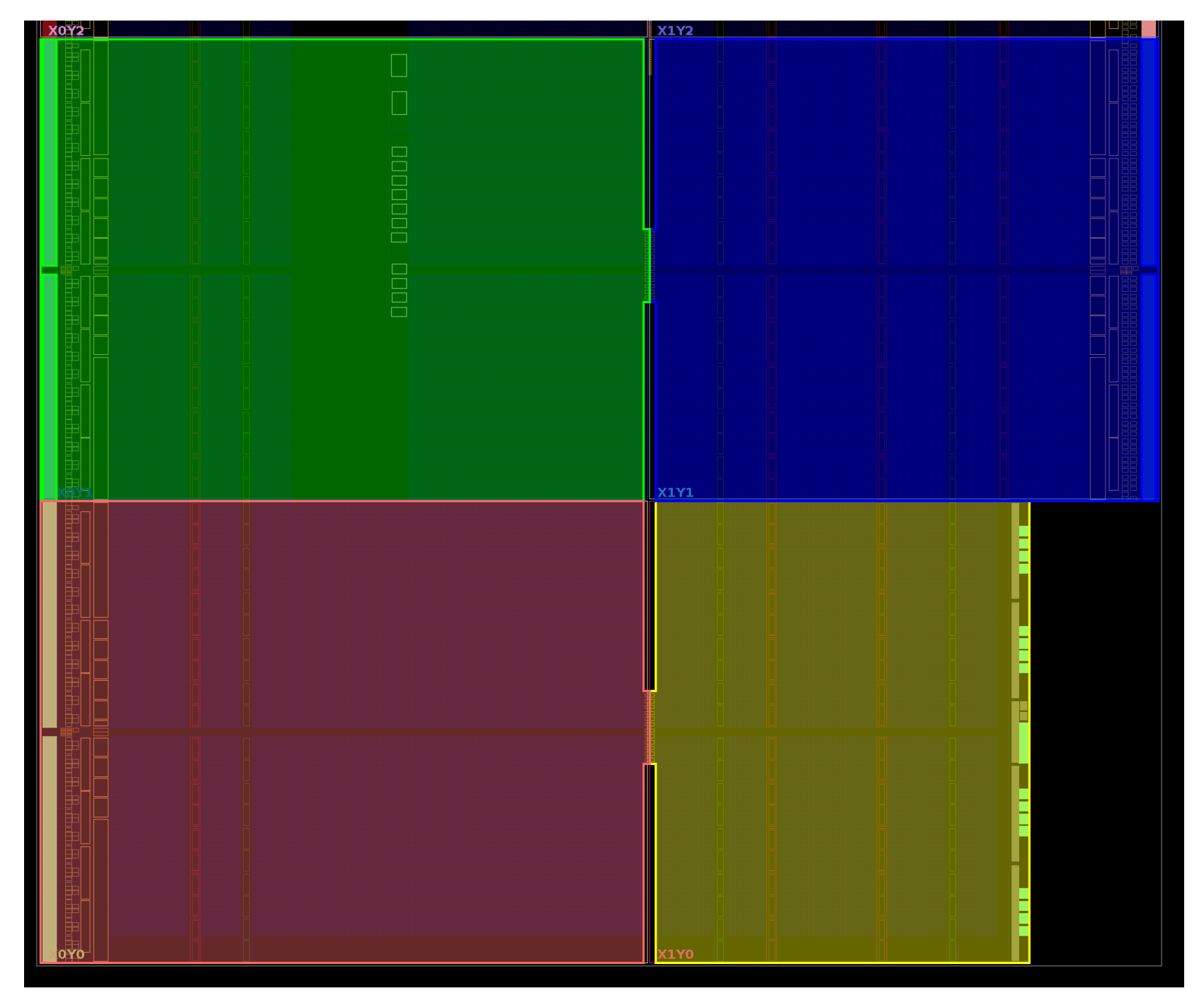
Within 28 nm 7-Series Xilinx devices, as represented in
Figure 5, logical resources are systematically arranged within Configurable Logic Blocks (CLBs) split in two slices (i.e., SLICEM and SLICEL). As represented in
Figure 6, SLICEs contain diverse logic circuits, such as four Look-Up Tables (LUTs), eight FFs, and one carry logic primitive (CARRY4) [
33]. Each CARRY4 primitive has four outputs (numbered 0 to 3), for each two distinct signals that are available, the CO and the O, which for our purposes are each the negation of the other. The CO and O outputs can be sampled mutually exclusively by the corresponding lettered FF (i.e., CO[0] and O[0] to AFF, CO[1] and O[1] to BFF, CO[2] and O[2] to CFF, CO[3] and O[3] to DFF). The CARRY4 thus functions as a four-tap TDL that propagates the input signal from the bottom to the top of the SLICE (i.e., from CO[0] and O[0] to CO[3] and O[3]). Notably, for the facilitation of clock routing, the FPGA is discretely partitioned into
CLBs clock regions [
34] (
Figure 7), wherein the clock skew into CLBs (i.e.,
) is negligible while the CRC one is not (i.e.,
).
The fundamental structure of the TDL-TDC taken as reference is instantiated in a Xilinx Artix 100T device putting in series
CARRY4 primitives, used as taps, sampled by FFs (
Figure 6). This results in a
-tap long TDL, where the total number of taps
N is 4 times the number of carry primitives
(i.e.,
), complemented by real-time decoder and calibration mechanisms [
11]. For practical use in real-world applications, the TDL-TDC, following the Nutt Interpolation architecture exposed in the Introduction, must be combined with a coarse counter; in our case an 8-bit counter (i.e.,
). Consequently, the total delay introduced by the TDL (i.e.,
) must be greater than or equal to the clock period of the coarse counter (i.e.,
). Considering that the 28 nm technology node of the Xilinx 7-Series is characterized by an average propagation delay (
) of approximately 15 ps (i.e.,
) for the elements composing the CARRY4 logic (i.e.,
), and that the maximum clock frequencies for a complex firmware are around 400–500 MHz (i.e.,
[2 ns; 2.5 ns]) [
35], it becomes necessary to use TDLs composed, approximately, of more than 168 taps (i.e.,
), corresponding to
. However, the TDL must be sufficiently lengthy to ensure ample margin to accommodate variations in the average propagation delay due to process, voltage, and temperature (PVT).
Although faster clocks (i.e., shorter TDLs) may seem plausible, the system’s fully integrated design confines us to a clock period of 2.4 ns and a 256-tap long TDL (i.e.,
); in this way, thanks to the Nutt Interpolation the FSR is extended up to 614.4 ns (i.e.,
ns).
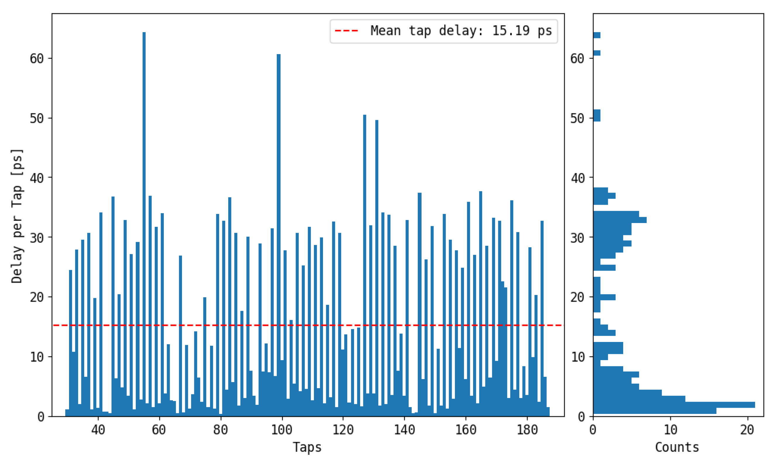
Figure 8 shows an example of the CT of the implemented TDL-TDC and the related probability density function of delays
. From
Figure 8, it can be observed that only 190 out of the 256 available taps are effectively utilized, defining an average propagation delay of 15.19 ps. Additionally, a significant dispersion in propagation delays is evident, ranging from a minimum of 1 ps to a maximum of 63 ps. It is also noticeable that the probability density function of delays
does not follow a specific normal shape, which is consistent with observations reported in other studies [
36,
37].
For experimental purposes, the above-described Nutt-Interpolated TDL-TDC was implemented in a specific module called FELIX [
38] provided by TEDIEL S.r.l. [
39], which hosts a Xilinx 28 nm 7-Series Artix-7 100T FPGA. The 256-bit long thermometer codes generated by the TDL and the contents of the 8-bit long coarse counter are sent to a Personal Computer (PC) via USB 2.0, which performs over the sum1s decoding algorithm, the calibration process, the Nutt Interpolation, and also the BE correction.
3. Bubble Error Analysis
As stated in the introduction, the only BEs that can be corrected are the deterministic ones due to the skew (i.e., and ) on the clock line (i.e., STOP signal) and routing delays (i.e., ) between the buffer outputs and the corresponding FF inputs. This was performed by experimental derivation and is expressed in terms of the so-called Bubble Length (BL), also known as , which is the number of taps involved in the artifact. In fact, the larger the BL, the greater the value of the skew and routing delays compared to the tap propagation time, thus the greater the negative influence of the BEs on the time measurement.
First, we studied the contribution of skew on the clock line (i.e.,
and
) by placing a 256-tap long TDL (i.e.,
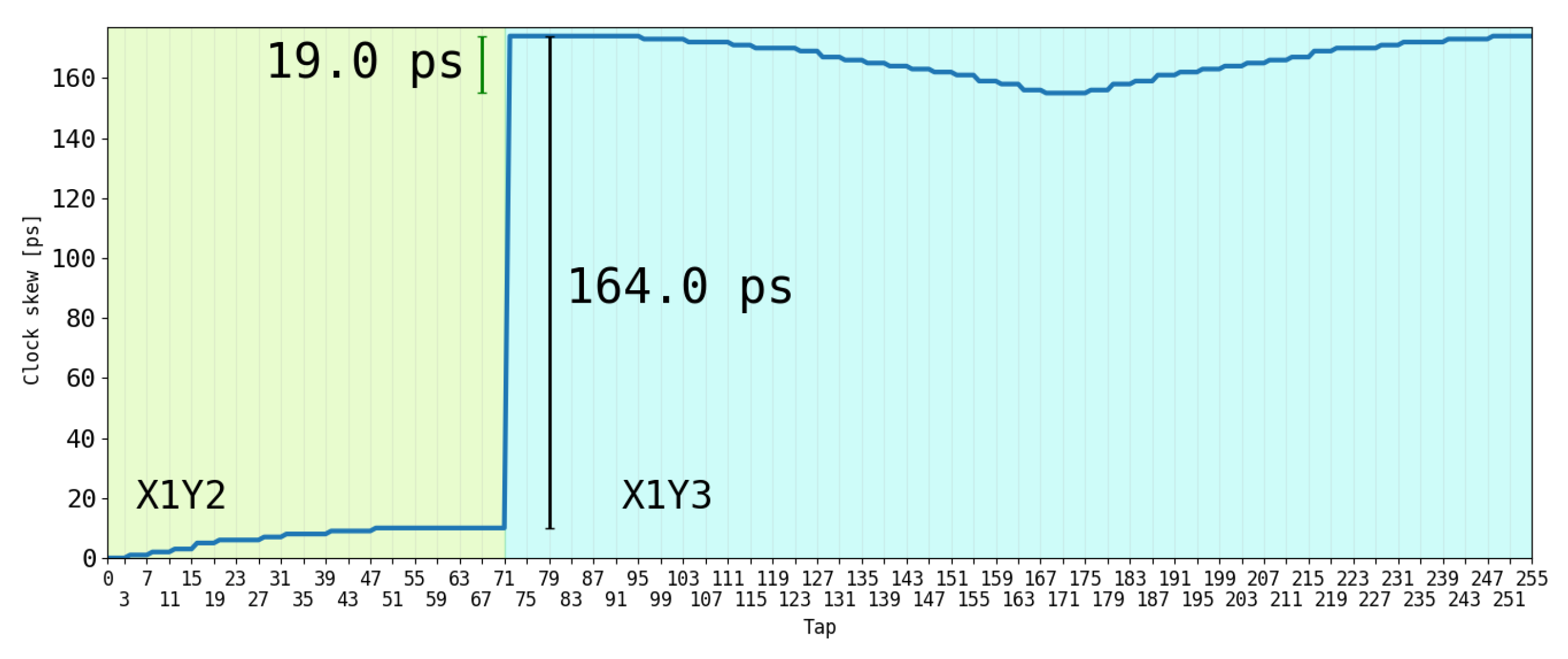
) across two contiguous CRCs, so that the first 18 CARRY4 blocks (72 taps, from tap 0 to tap 71) were in one CR and the next 46 (184 taps, from tap 72 to 255) in the following one. We obtained the clock skew of each tap in the TDL using the Vivado post-implementation timing analysis tool in order to better examine how the clock propagates in that area.
Figure 9 shows the overall skew present at the clock input of the 256 FFs that sample the 256 taps, taking the clock input of tap 0 as zero. Within the CR hosting the second portion of the TDL (i.e., from tap 72 to 255), the skew ranges between 178 and 159 ps (a delta of 19 ps), with the minimum at tap 171, which is at the middle of the CR. In contrast, the skew present at the CRC (i.e., between tap 71 and tap 72) is an order of magnitude higher, amounting to 164 ps. This agrees with the information in [
34], which states that the clock is propagated in a tree-like manner between CRs and injected in the middle of each. In this sense, it is possible to easily identify the magnitude of
, which is 164 ps. Instead, regarding
, we observe that in 100 taps from tap 72 to 171 (i.e., half a CR, 25 CLBs with one CARRY4 each), only a skew of 19 ps is accumulated. This means that, if we consider
constant over
k and equal to
(i.e.,
),
is approximately 0.19 ps (i.e.,
/100 = (19 ps)/100 and negligible with respect to
and the average propagation delay of the buffer (i.e.,
= 15 ps). Unlike
(i.e., 0.19 ps), we clearly notice that
(i.e., 164 ps) is much greater, and thus not negligible compared to
(i.e., 15 ps).
Using Vivado’s post-implementation timing analysis, regarding the routing delays (i.e., ), an ideal delay of 0 ps is provided. Although the actual value will be greater than the declared 0 ps, this information is sufficient to tell us that such a delay can be approximately neglected.
In this sense, we easily deduce that the BEs with larger BL are mainly due to
because it is the biggest non-ideality. This causes deterministic BEs with a larger BL proportional to
(i.e.,
). This is due to the signal propagating asynchronously over the TDL after CRC, being sampled with a delay of
with respect to the taps before the CRC. We call it BEs-CRC. While not being classified as a form of BE, the results of this effect were already seen in [
19]. In this regard, the taps that provide a total propagation delay equal to
before the CRC (orange in
Figure 10) and the subsequent ones (blue in
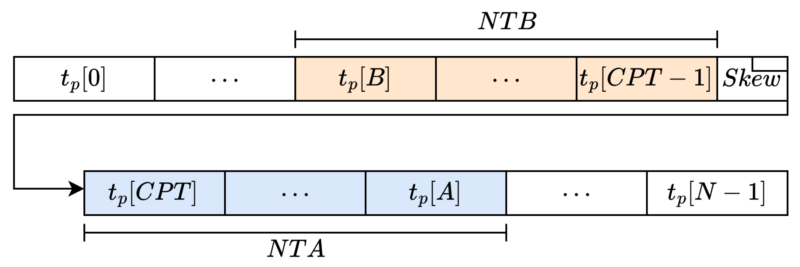
Figure 10) offer the same information. So, we define the Crossing Point Tap (CPT) as the first tap after the CRC (e.g., tap
in
Figure 3, tap 72 in
Figure 9 and
Figure 11). Thus, before and after the CPT, we have two sections of the TDL with a temporal duration of approximately
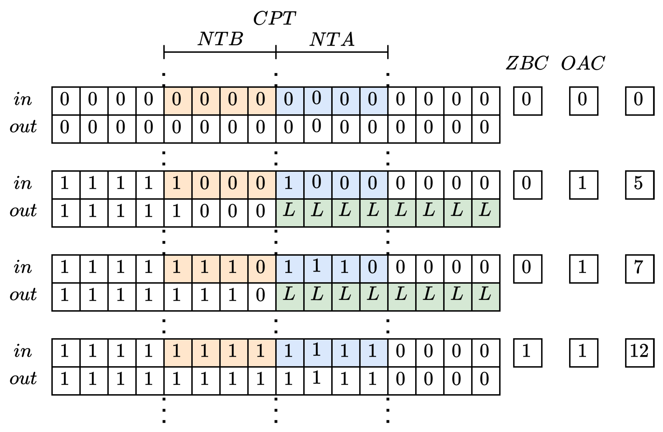
that, due to the skew, will carry the same information; these are referred to as Causal and Anti-Causal. Consequently, in terms of bins, we call these lengths Number of Taps Before the CRC (NTB) and Number of Taps After CRC (NTA) for the Causal and Anti-Causal sections, respectively.
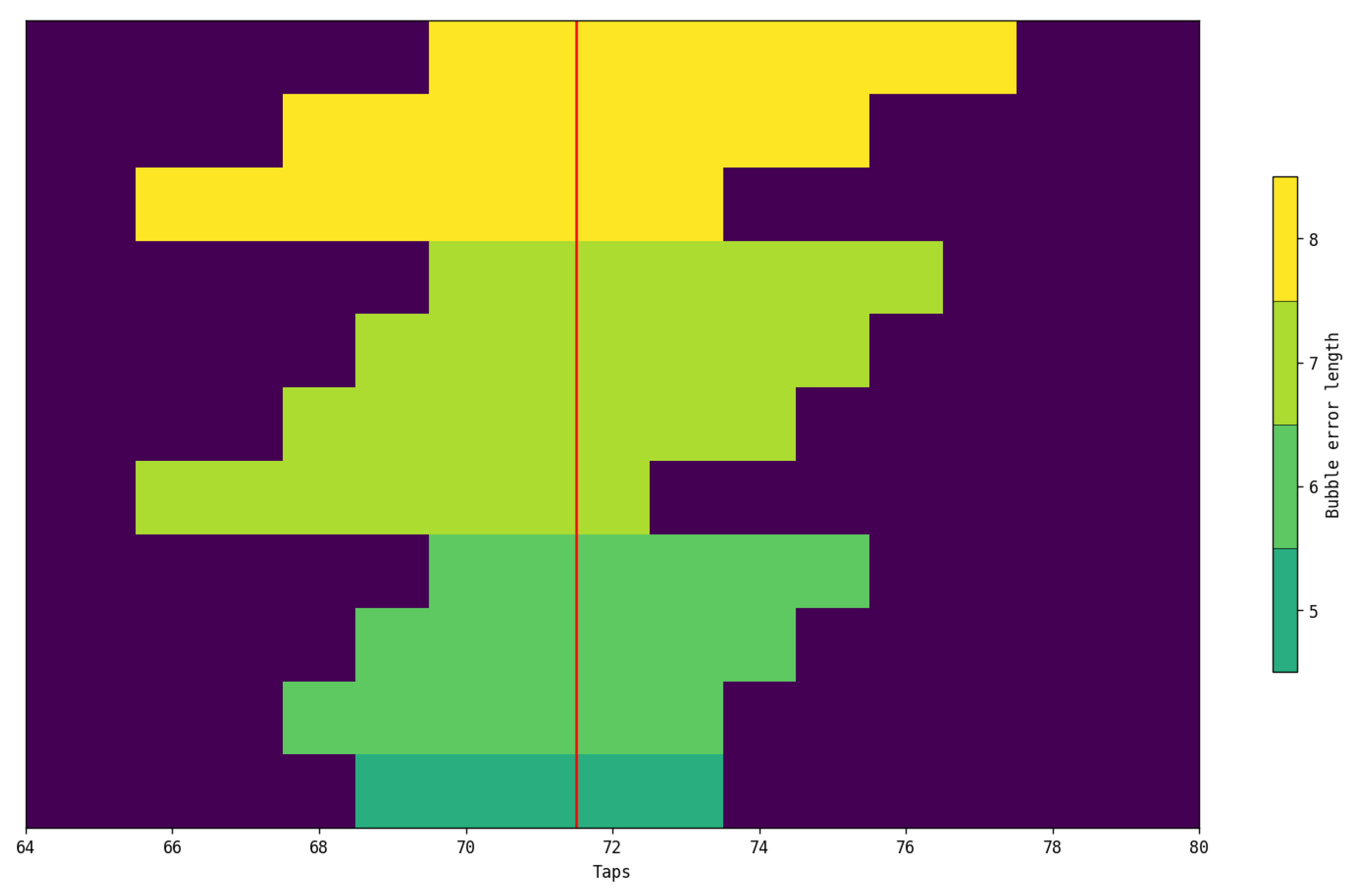
All this was also demonstrated experimentally by acquiring several thermometric codes (i.e.,
) from the analyzed TDL, verifying that the BEs with larger BL occur at the CRC. For demonstration purposes,
Figure 11 shows the 11 thermometric codes with the largest BL (i.e.,
dark green,
green,
lime, and
yellow) from the TDL studied in the post-implementation stage, and it is observed that these BEs are concentrated in the CRC. It can be observed that these BEs extend, before the CRC, from tap 66 to tap 71 and after the CRC from tap 72 to tap 7, that is, for 6 taps before (i.e.,
) and 6 taps after (i.e.,
) the CRC, thus allowing for the easy identification of the redundant informational content portions around the CRC (i.e., Causal and Anti-Causal sections of the TDL), highlighted in orange and blue in
Figure 10. Furthermore, comparing
Figure 10 with
Figure 11, we can experimentally derive that
Moreover, knowing that each tap provides an average delay of 15 ps (i.e., ps), we can estimate as the product between NTB or NTA and , obtaining 90 (i.e., ps), consistent with the 164 ps from the post-implementation analysis.
Also, Equation (
5) provides a theoretical explanation to larger BEs-CRC shown in
Figure 11. In accordance with the scientific literature [
40], in our specific case, we have a negligible
and
with respect to a
of a few hundred ps (i.e.,
= 164 ps) (
Figure 9) and a propagation delay (
Figure 8) between a few ps and tens of ps with an average value of 15 ps (i.e.,
ps). Considering that
and that
ps, we can rewrite (
5) as follows:
Moreover, from Equation (
8), considering that
we derive
By observing Equation (
9), we deduce that we can see CRC-BEs if
is bigger than
; moreover, we can theoretically estimate the NTA and NTB lengths as
obtaining a value of
taps in accordance with experimental measurements reported in
Figure 11. This estimation becomes increasingly accurate the larger the
is compared to the average propagation time (i.e.,
), and the less dispersed the propagation time of the taps in the Causal and Anti-Causal sections of the TDL tends to be.
4. Clock Region Crossing Bubble Error Correction
This section describes an offline technique that makes it possible to correct the CRC-BEs. This technique is executed over the PC on the acquired thermometric codes before performing the sum1s decoding and the calibration. By examining just the thermometer code sampled by the TDL-TDC, we may abstract the idea presented in
Figure 10 into
Figure 12, highlighting the TDL taps belonging to the Causal portion (i.e., from tap
B to tap
with
) and the Anti-Causal portion (i.e., from tap
to tap
A with
) of the TDL. Referring to the physical implementation of the TDL analyzed in
Section 3, we recall that
,
, thus,
66 and
.
Algorithm 1 encodes the information about the Causal (i.e., the number of zeros inside the NTB) and Anti-Casual (i.e., the number of ones inside the NTA) using variables Zero Before Crossing (ZBC) and One After Crossing (OAC), respectively, in order to reject the BEs-CRC; thus, if the BEs-CRC is asserted (i.e.,
and
) the section of the TDL after the CPT (so, the Anti-Casual) is forced to zero. In this way, only the timing information over the Casual part is used.
| Algorithm 1 Detection of the BEs-CRC. |
|
A functional example is provided in
Figure 13 where only the first thermometric code and the last one are bubble-free. With second and third codes, the algorithm detects the bubble and disables the last part of the TDL (L in figure). This leads to a certain amount of missing taps depending on NTA/NTB, in this case 8 to 11, which reduces the number of output codes from 16 to 12.
The effectiveness of the proposed strategy implemented in Algorithm 1 has been checked offline, via software, by obtaining and then comparing CTs with and without the correction of the BEs-CRC reading out the TDL. The CT obtained without correction of the BE-CRCs using a sum1s decoder is shown in
Figure 14a. Meanwhile, the corrected CT downstream is represented in
Figure 14c. Instead,
Figure 14b,d show a zoom of the Causal section of the TDL.
Putting the correction into practice as the algorithm specifies the Anti-Causal section of the TDL (i.e., from tap 72, CPT, to 77, A, highlighted in red in
Figure 14c) has propagation delays equal to zero. This is because they are no longer valid outputs for the TDL-TDC and are not considered by the calibration algorithm. On the other hand, if we observe the uncorrected CT (
Figure 14a), we notice that it is identical to the corrected one except for the Causal part, which provides propagation delays that are on average a factor of 2 faster (i.e., ≈7 ps) (
Figure 14b) than elsewhere (
ps).
An explanation for the findings points to an order-2 sub-interpolation effect [
13,
28] between Casaul and Anti-Causal sections of the TDL. Essentially, if we consider the Anti-Causal section as a delayed replica of the Causal one, the impact becomes more evident (
Figure 15). Indeed, if an uncorrected BEs-CRC occurs, it means that we are simultaneously decoding two pieces of information from the same measurement interval, one from the NTA and one from the NTB, which will be sub-interpolated (i.e., added) among each other in the sum1s decoding like a WUA [
28,
32]. This gives rise to an unexpected order-2 intra-TDL sub-interpolation effect that helps to increase the resolution only if the sub-interpolated bins are properly mapped in the Anti-Causal section.
The results would have been quite different if, instead of a bubble compression-based decoder like sum1s, we had used a transition-based decoder like Log2. In fact, in that case, the Causal portion of the TDL would be completely masked by the Anti-Causal portion, effectively eliminating the order-2 intra-TDL sub-interpolation effect.
5. Experimental Results
In this section, the precision and the quantization error offered with and without the correction of the CDC-BEs, considering different values of NTA = NTB (i.e., 1, 2, 6, and 8), are measured. The precision was evaluated as the standard deviation of the timestamps, in our case a pool of measurements, provided by the Nutt-Interpolated TDL-TDC in measuring a constant time delay, defined between a START signal and a STOP signal. Meanwhile, the quantization error was calculated using the provided by the TDL independently to the time delay. It was decided to vary the values of NTA and NTB to better observe the behavior of Algorithm 1 for the BEs-CRC correction. To minimize potential dependencies between precision and the measured time interval, the precision of the TDL-TDC was evaluated as a function of the time interval between START and STOP.
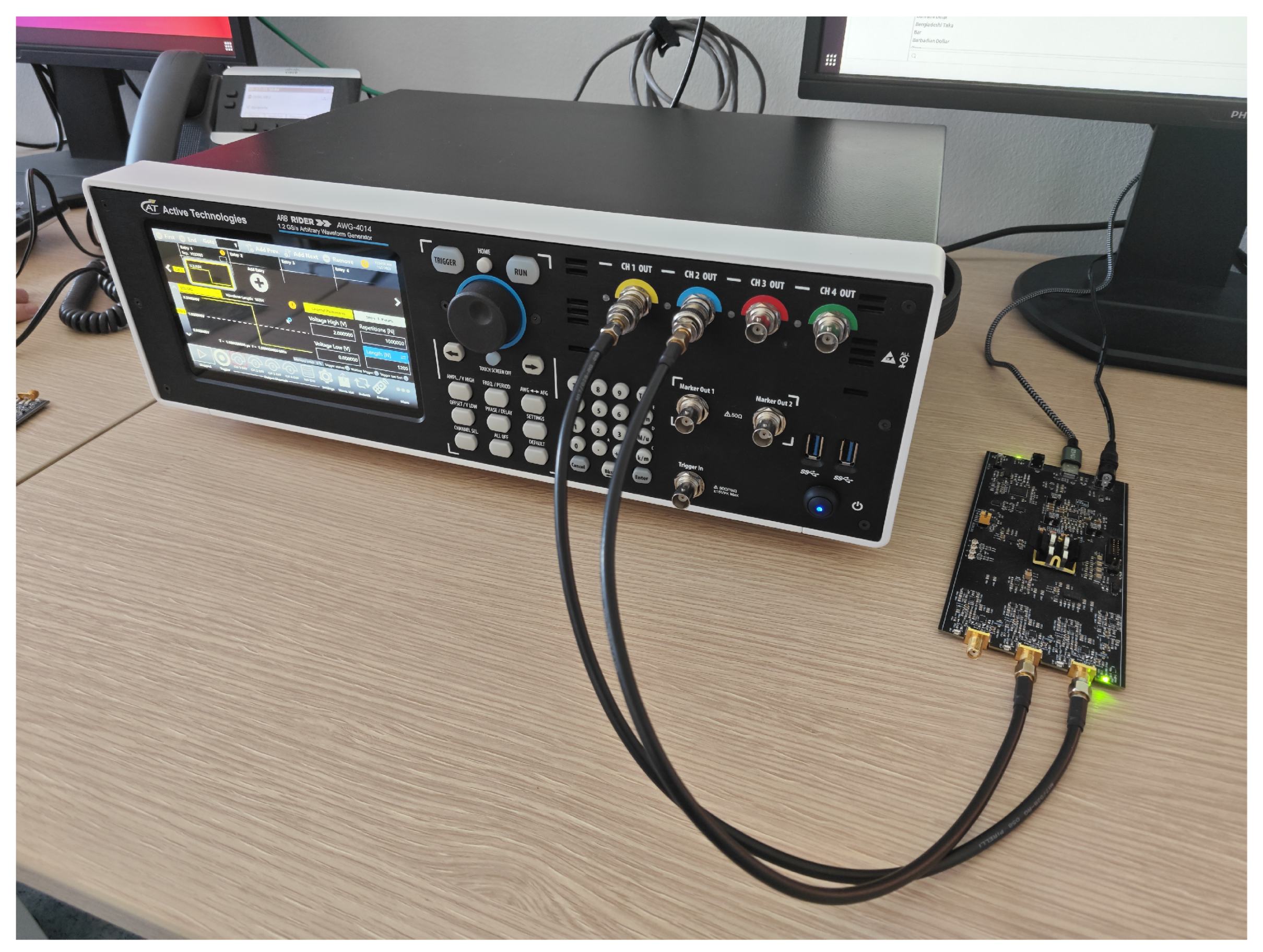
The START and STOP signals (i.e., two coaxial cables in
Figure 16) were generated using the ACTIVEAWG401X [
41] (black box with monitor in
Figure 16) in delay sweep mode from −0.5 ns to 16.8 ns with step of 50 ps. The 256-tap long TDL-TDC and the 8-bit long coarse counter presented in Section have been implemented in a Xilinx 28 nm 7-Series Artix 100T FPGA (i.e., FELIX [
38] provided by TEDIEL S.r.l. [
39], black printed circuit board in
Figure 16), while the Algorithm 1 together with the sum1s decoding, calibration, and Nutt Interpolation are performed on a PC. Both the thermometer codes from the TDL and the coarse counter values needed for the Nutt Interpolation are transmitted to the PC via USB 2.0.
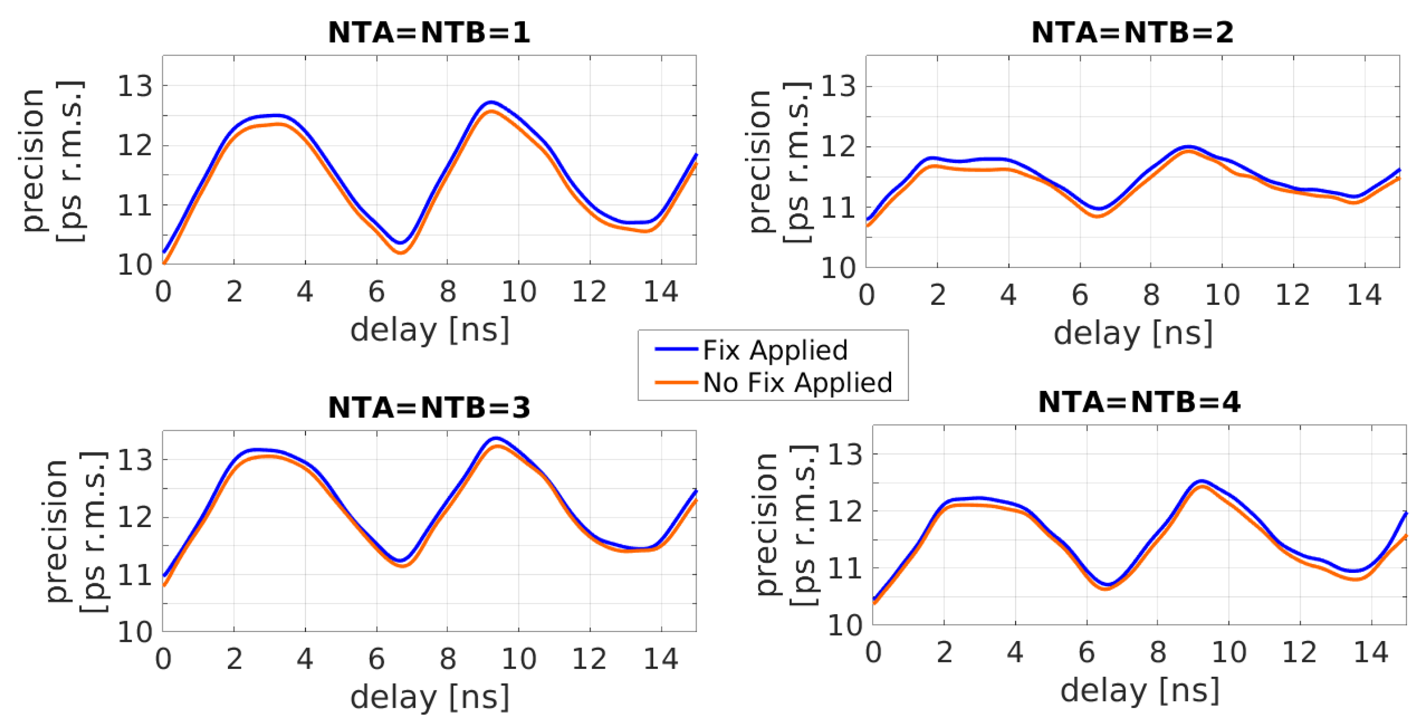
Referring to the Casual and Anti-Casual portions, we know, from
Section 4, that
and
. Consequently, as
Figure 17 shows, we have evaluated the precision as function of the time delay between the START and the STOP, using different values of NTA = NTB. In orange, the uncorrected solution, and in blue, the corrections with
, as computed in
Section 2, and with bigger (i.e.,
) and lower (i.e.,
and
) values.
Furthermore, upon examining
Figure 17, one can quickly observe the absolute decrease in the precision of the uncorrected scenario (orange), which underscores the precision gain advantage of sub-interpolation between the Causal (i.e., from tap
to tap
) and Anti-Causal (i.e., from tap
to tap
) portions of the TDL as mentioned in
Section 4.
Table 1 offers an overview of all the results and emphasizes the differences in TDL-TDC maximum (i.e., Max
), minimum (i.e., Min
), and mean precision (i.e., Mean
) with and without BEs-CRC correction.
Table 2 illustrates a comparison of the theoretical precision (i.e., the quantization error,
) [
13], computed as the quantization errors offered by the TDL-TDC with (i.e.,
), and without (i.e.,
), the BEs-CRC and, their spread
(i.e.,
). We can observe that
is compatible with the experimental results exposed in
Table 1 (i.e., Mean
).
In this way, we have demonstrated how the order-2 intra-TDL sub-interpolation effect, investigated in
Section 4, positively impacts the measurement precision by reducing the quantization error. By observing
Table 1 and
Table 2, we can note that if we select arbitrary values for NTA and NTB, different from the Causal and Anti-Causal portions of the TDL, we increase the quantization error, thereby reducing the precision.


 ,
, 


