Article

A Temperature-Independent Gate-Oxide Degradation Monitoring Method for Silicon Carbide Metal Oxide–Semiconductor Field-Effect Transistors Based on Turn-Off Ringing

by
Xinghao Zhou
,
Pengju Sun
*,
Kaiwei Li
,
Qingsong Liu
,
Lan Chen
and
Bo Wang
The State Key Laboratory of Power Transmission Equipment Technology, Chongqing University, Chongqing 400044, China
*
Author to whom correspondence should be addressed.
Electronics 2025, 14(4), 771; https://doi.org/10.3390/electronics14040771
Submission received: 10 January 2025 / Revised: 25 January 2025 / Accepted: 13 February 2025 / Published: 16 February 2025

Abstract

:
Gate-oxide degradation in silicon carbide (SiC) metal oxide–semiconductor field-effect transistors (MOSFETs) is a significant concern. Consequently, several methods have been developed to monitor the aging degree. In this article, a temperature-independent method for gate-oxide degradation monitoring is proposed by measuring the minimum turn-off circuit parasitic inductor voltage vcir_min at a specific gate resistor and voltage. The temperature sensitivity of vcir_min is analyzed based on a derived model. Adjustment of the turn-off gate voltage and resistance is proposed to mitigate the impact of temperature on vcir_min. The devices under test are aged by high-temperature gate bias (HTGB) experiments and are tested in double-pulse tests (DPT). A 32 V bias for 42 h and 25–150 °C temperature results in changes of 6.55% and 0.103% in vcir_min, respectively. The experimental results show that the proposed method is effective in maintaining temperature independence. Additionally, the effects of bus voltage, load current, and bond wire failure on vcir_min are also tested and analyzed. The proposed method provides a valuable tool for accurately monitoring SiC MOSFET gate-oxide degradation in scenarios characterized by significant temperature fluctuations.

1. Introduction

SiC MOSFETs exhibit higher withstand temperatures, faster switching speeds, and lower on-resistance compared to conventional Si-based devices [1]. Consequently, their market share is rapidly increasing in sectors such as new energy generation, electric vehicles, and power supplies. However, due to the high interface state density and time-dependent dielectric breakdown (TDDB) of SiC MOSFETs, the gate-oxide reliability of SiC MOSFETs is one of the main obstacles to their large-scale marketization [2]. In particular, the threshold voltage (VTH) drift, i.e., bias temperature instability (BTI), has been widely discussed [3]. Therefore, it is essential to monitor the gate-oxide degradation of SiC MOSFETs to ensure reliable performance in critical applications.
The variations in electrical parameters are the primary indicators of gate-oxide degradation. Several methods have been proposed to monitor gate-oxide degradation through either direct or indirect measurements of electrical parameters. The drift of VTH is widely recognized as a direct reflection of BTI. However, measuring VTH is both costly and challenging despite the fact that VTH experiences significant drift as the gate-oxide degrades [4,5]. Furthermore, the high temperature sensitivity of VTH complicates accurate monitoring during temperature fluctuations [6,7]. On-resistance (RON) and body diode voltage drop (VSD) vary with the drift of VTH as the gate oxide degrades [8,9]. A method for monitoring SiC MOSFET gate-oxide degradation based on RON in the saturated region is described in [9]. However, this method is only suitable for in situ monitoring, as it cannot eliminate disturbances caused by temperature variations. An alternative approach, which involves simultaneously measuring VTH and RON and constructing feature-target functions to mathematically decouple temperature and aging, was proposed in [6]. Nevertheless, the challenges associated with VTH measurement remain unresolved with this method. The degree of gate-oxide degradation is also reflected by the VSD at 0 V gate voltage [10]. Similar to RON, VSD, as a monitoring precursor, is still susceptible to temperature effects. Furthermore, measuring VSD at 0 V gate voltage is relatively complex. The Miller voltage plateau (VGP) and Miller plateau time (tGP) exhibit a linear relationship with the logarithmic stress time during the gate-oxide degradation [11,12]. However, the rapid on/off switching of SiC MOSFETs and oscillations in the Miller plateau complicate the measurement of VGP and tGP. Additionally, due to the strong correlation between VGP and VTH, the influence of temperature cannot be disregarded.
The TDDB of the SiC MOSFET gate oxide layer under high temperature and high electric field stress leads to an increase in gate leakage current (Igss) [13]. An early warning method for detecting SiC MOSFET gate-oxide degradation based on Igss is presented in [14]. The Igss exhibits very low temperature sensitivity at low gate voltages. However, it is not until the later stages of the gate’s lifespan that Igss shows a significant increase, rendering it suitable only for fault warning purposes. Additionally, the mA level changes in Igss also lead to measurement challenges. The junction capacitance at low drain-source voltage (vDS) and low gate voltage (vGS), which is another temperature-independent precursor for monitoring the gate-oxide degradation, is presented in [15]. However, challenging measurements at low vDS and vGS can still be addressed for junction capacitance used in degradation monitoring. An innovative method that converts the gate input capacitance (Ciss) magnitude to gate charge time is proposed in [16]. However, it is still challenging to measure time variations on the order of ns due to the changes in the order of pF in Ciss caused by gate-oxide degradation.
The gate-oxide degradation monitoring methods for SiC MOSFETs mentioned above either fail to decouple from temperature influences or present significant measurement challenges. Additionally, the intrusiveness to the system is also increased due to the necessity of interfacing with the monitoring object pins for measuring. Therefore, there is a pressing need to identify a method that is unaffected by temperature and allows for straightforward online measurements. Furthermore, it is essential to minimize the intrusiveness to the system. The current change rate (di/dt) is widely recognized as a temperature-sensitive electrical parameter in IGBT and MOSFET junction temperature (Tj) measurements due to its established measurement techniques and good linearity [17,18,19,20,21,22]. The change rate of drain-source current (diDS/dt) during turn-on is proposed as a nearly temperature-independent precursor for monitoring the gate-oxide degradation of SiC MOSFETs [23]. However, many studies have demonstrated that turn-on diDS/dt is closely related to Tj due to its correlation with the VTH [20,24]. The positive temperature sensitivity of Coulomb-scattered carrier mobility (μC), which dominates the carrier effective mobility (μ) at low vGS, has been discussed in [25,26]. For turn-off diDS/dt, there exists an antagonism between the positive temperature sensitivity of μC and the negative temperature sensitivity of VTH. Thus, turn-off diDS/dt has the potential to serve as a monitoring precursor that eliminates the effects of temperature.
This article investigates the effects of gate-oxide degradation and temperature on the minimum turn-off diDS/dt. The relationship between gate resistance (RG), turn-off gate voltage (VEE), and temperature sensitivity is analyzed. At appropriate values of RG and VEE, low temperature sensitivity is observed, along with a significantly greater degradation sensitivity compared to temperature sensitivity. In addition, the minimum turn-off diDS/dt can be periodically measured through minimum circuit parasitic inductance voltage (vcir_min), thereby minimizing the impact of monitoring on the system. The measurement difficulties can be reduced by using a peak detection circuit [18,22]. The effectiveness of the method for temperature-independent gate-oxide degradation monitoring of SiC MOSFETs is validated using the double-pulse test. The rest of the article is organized as follows. Section 2 explains the mechanisms by which the gate-oxide degradation and temperature affect vcir_min and analyzes the roles of varying VEE and RG in mitigating temperature disturbances. In Section 3, the criteria for selecting VEE and RG are presented. The validity of the proposed method is verified using the double-pulse test. Additionally, the impact of various factors on the proposed method is discussed. Section 4 provides a universal analysis, along with a comparison to other precursors. Finally, the content of the article is concluded in Section 5.

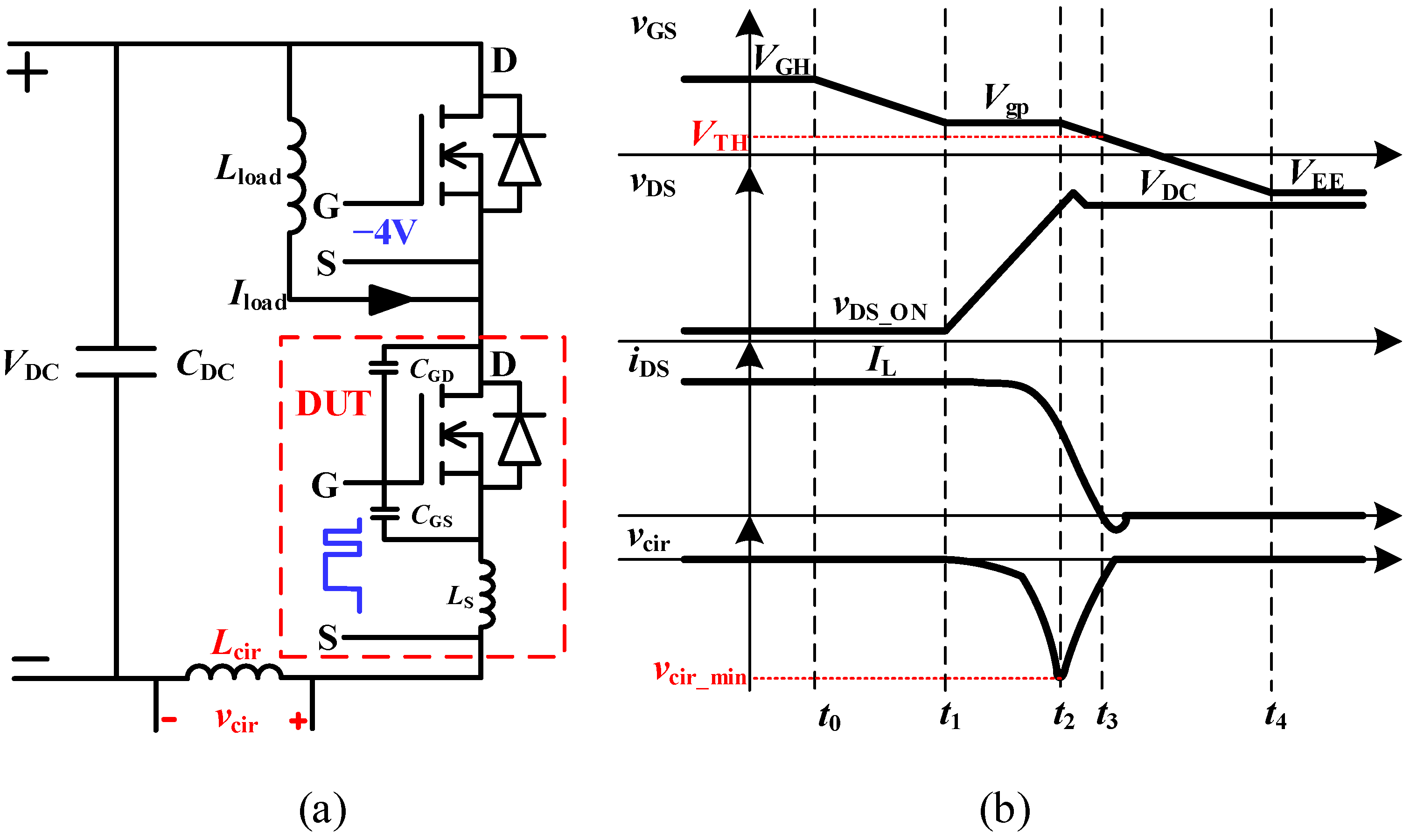
2. Theoretical Basis of the Proposed Gate-Oxide Degradation Monitoring Method

2.1. The vcir_min of SiC MOSFET at Turn-Off

In this section, the turn-off process of SiC MOSFET, which can be divided into four stages, is analyzed, and the vcir_min is derived using fundamental device equations. The schematic circuit and turn-off process of SiC MOSFET are shown in Figure 1. LS and Lcir are the source parasitic inductance and part circuit parasitic inductance, respectively. CDC, CGS, and CGD are the bus capacitance, gate-source parasitic capacitance, and gate-drain parasitic capacitance, respectively.
When a turn-off signal is transmitted from the control system to the driver at t0, the drive voltage switches from positive voltage (VGH) to negative voltage (−VEE). The charges stored in the gate input capacitance Ciss are released through the gate drive resistor RG. The gate-source voltage (vGS) can be expressed as
v GS ( t ) = V G exp ( t R G C iss ) V EE L S d i DS ( t ) d t
where
C iss C GS + C GD             V G = V GH + V EE
At t1, the vGS reaches the Miller plateau voltage (VGP), which can be expressed as [11]
V GP = V TH + 2 I L L CH μ C OX W CH
where LCH is the channel length, WCH is the channel width, μ is the carrier mobility of the channel, and COX is the gate oxide capacitance per unit area.
At t3, the drain source (vDS) reaches the bus voltage (VDC). Then, the vGS continues to drop, according to (1). At the same time, the channel begins to shut down, accompanied by a decrease in drain-source current (iDS), in accordance with [24]
i DS ( t ) = B μ 2 ( v GS ( t ) V TH ) 2
where B is expressed as
B = W CH C OX L CH
The drain-source current change rate (diDS/dt) in this phase can be obtained by differentiating iDS with respect to t.
d i DS d t = B μ ( v GS ( t ) V TH ) V G R G C iss exp ( t R G C iss ) L S d 2 i DS ( t ) d 2 t
When diDS/dt reaches the minimum value, d2iDS/d2t = 0. Based on (1) and (6), the time derivative of diDS/dt is given by
d 2 i DS ( t ) d 2 t = B μ V G ( R G C iss ) 2 exp ( t R G C iss ) × 2 V G exp ( t R G C iss ) + V EE + V TH + L S d i DS ( t ) d t
At t3, vGS reaches VTH, which causes the inversion layer to disappear and the iDS to decrease to 0. At this time,
V G exp ( t 3 R G C iss ) = V EE + V TH + L S d i DS ( t 3 ) d t
Based on (6) and (8), the d2iDS/d2t at t3 can be rewritten as
d 2 i DS ( t 3 ) d 2 t 3 = B μ V G ( R G C iss ) 2 exp ( t 3 R G C iss ) V EE + V TH
The d2iDS/d2t > 0 at t3 based on (9). According to (7), in the interval t2-t3, the d2iDS/d2t decreases monotonically. Therefore, d2iDS/d2t > 0 in the interval t2-t3 means the diDS/dt continues to increase. Consequently, the value of the diDS/dt will reach its minimum (diDS/dt)min at t2. The (diDS/dt)min can be expressed based on (1), (3), and (6) as follows:
d i DS d t min = 2 I L + 2 B I L μ ( V TH + V EE ) L S 2 B I L μ + R G C iss
Furthermore, (10) can be obtained by establishing and solving the Kirchhoff voltage equations for the gate loop and power loop [27].
The circuit parasitic inductor voltage vcir can be expressed as follows:
v cir = L cir d i DS d t
The minimum circuit parasitic inductance voltage vcir_min corresponding to (diDS/dt)min can be expressed as follows:
v cir _ min = 2 L cir I L + L cir 2 B I L μ ( V TH + V EE ) L S 2 B I L μ + R G C iss
Following the t3, the vGS continues to decrease until it reaches the −VEE at t4.

2.2. Effects of Gate-Oxide Degradation and Temperature on vcir_min

According to (12), the vcir_min is a function of the VTH. Therefore, the vcir_min will exhibit a trend similar to VTH as the gate oxide degrades. The VTH can be expressed as follows:
V TH = ϕ ms Q trap C OX + 2 ψ B + 4 q ε SiC N A ψ B C OX
where q is the electron charge constant, εSiC is the dielectric constant of SiC, NA is the doping concentration in the p-type well, Qtrap is charge captured by traps per unit area, ψB is the Fermi potential, and ϕms is the work function difference of the interface.
When the gate of SiC MOSFETs is stressed, carriers are injected into the near-interface traps and oxide traps through quantum tunneling. The accumulation of Qtrap will lead to the BTI [2]. Specifically, the accumulation of captured negative charges would cause a positive shift in the VTH, which is called positive bias temperature instability (PBTI). Conversely, the accumulation of positive charges results in a negative shift, i.e., NBTI [16]. As negative charges captured accumulate, the vcir_min would decrease with accumulation time, and the accumulation of positive charges leads to an increase in vcir_min. In summary, the vcir_min, which varies with gate-oxide degradation, can be used as an effective monitoring precursor.
The effect of temperature on vcir_min needs to be further investigated to achieve temperature independence. According to (12), it is mainly VTH and μ in vcir_min that vary with temperature. The influence of temperature can be evaluated by taking the derivatives of (12) with respect to Tj:
d v cir _ min d T j = L cir B I L ( L S 2 B I L μ + R G C iss ) 2   2 I L L S R G C iss ( V TH + V EE ) 2 μ d μ d T j 2 L S μ B I L + R G C iss 2 μ d V TH d T j
The temperature sensitivity of VTH depends mainly on ψB, which can be expressed as [6]:
ψ B = k T j q ln N A n i = k T j q ln N A N C + E C E Fi q
where NC is the conduction state density, EC is the conduction energy, EFi is the intrinsic Fermi level, and k is the Boltzmann constant. The effect of Tj on the VTH can be described as [28]:
d V TH d T j = d ψ B d T j ( 2 + 1 C OX ε SiC q N A ψ B )
d ψ B d T j = k q ln ( N C N A )
In N-channel SiC MOSFETs, the NC is significantly larger than the NA, resulting in a negative temperature coefficient for the VTH, which has been extensively demonstrated in numerous studies [7].
On the other hand, the inversion layer exhibits a multitude of scattering mechanisms. The Coulomb scattering plays a dominant role in the μ during the switching of SiC MOSFET when the gate voltage is low [23,26]. Therefore, in the turn-off process, the μ can be considered as follows:
μ μ C
where μC is the Coulomb-scattered carrier mobility.
The temperature modeling of μC can be expressed as [28]:
μ C = N ( T j ) α ( Q inv ) β Q trap
where Qinv is the inversion charge, N is the model fitting parameter, α is the temperature coefficient, and β is the empirical coefficient. In the case of 4H-SiC, the values of α and β are typically set to 1.
The effect of Tj on the μ can be described as follows:
d μ d T j = N Q inv Q trap = μ T j
Based on (16) and (20), Equation (14) can be rewritten as
d v cir _ min d T j = L cir B I L μ ( L S 2 B I L μ + R G C iss ) 2   2 λ C iss C iss ( V TH + V EE ) 2 T j × R G + 2 I L L S 2 T j + 2 λ L S B I L μ                     = δ f ( V EE ) × R G + γ
where
δ = L cir B I L μ ( L S 2 B I L μ + R G C iss ) 2
f ( V EE ) = 2 λ C iss C iss ( V TH + V EE ) 2 T j
γ = 2 I L L S 2 T j + 2 λ L S B I L μ
λ = 2 + 1 C OX ε SiC q N A ψ B k q ln N C N A
According to (21), it can be found that the polarity of dvcir_min/dTj is related to the RG and VEE. RG and VEE are not typically designed specifically to monitor gate-oxide degradation. However, due to the long-term nature of gate-oxide degradation, the degradation monitoring does not need to be continuous during SiC MOSFET operation but only requires sampling with long time intervals [16]. Therefore, it is only necessary to switch to the RG_M and VEE_M required for monitoring at sampling, and the advent of intelligent drives could facilitate this approach [29]. To eliminate temperature disturbances, there are
d v cir _ min d T j = 0
According to (22)–(24), there are
δ > 0 γ > 0 f ( V EE ) > 0   or < 0
In accordance with (21), the sufficiently necessary condition to satisfy (26) is
f ( V EE ) < 0   f ( V EE ) × R G = γ
From (23), it can be inferred that the condition f(VEE) < 0 is
V EE _ M > 2 λ T j V TH
When the VEE_M is deterministic, there always exists a specific RG (i.e., RG_M) that satisfies −f(VEE_MRG_M = γ. Therefore, there will always be VEE_M and RG_M to ensure dvcir_min/dTj = 0. In conclusion, when the optimal values of VEE_M and RG_M have been selected, the vcir_min can be used as a temperature-independent parameter to monitor the gate-oxide degradation of SiC MOSFET.

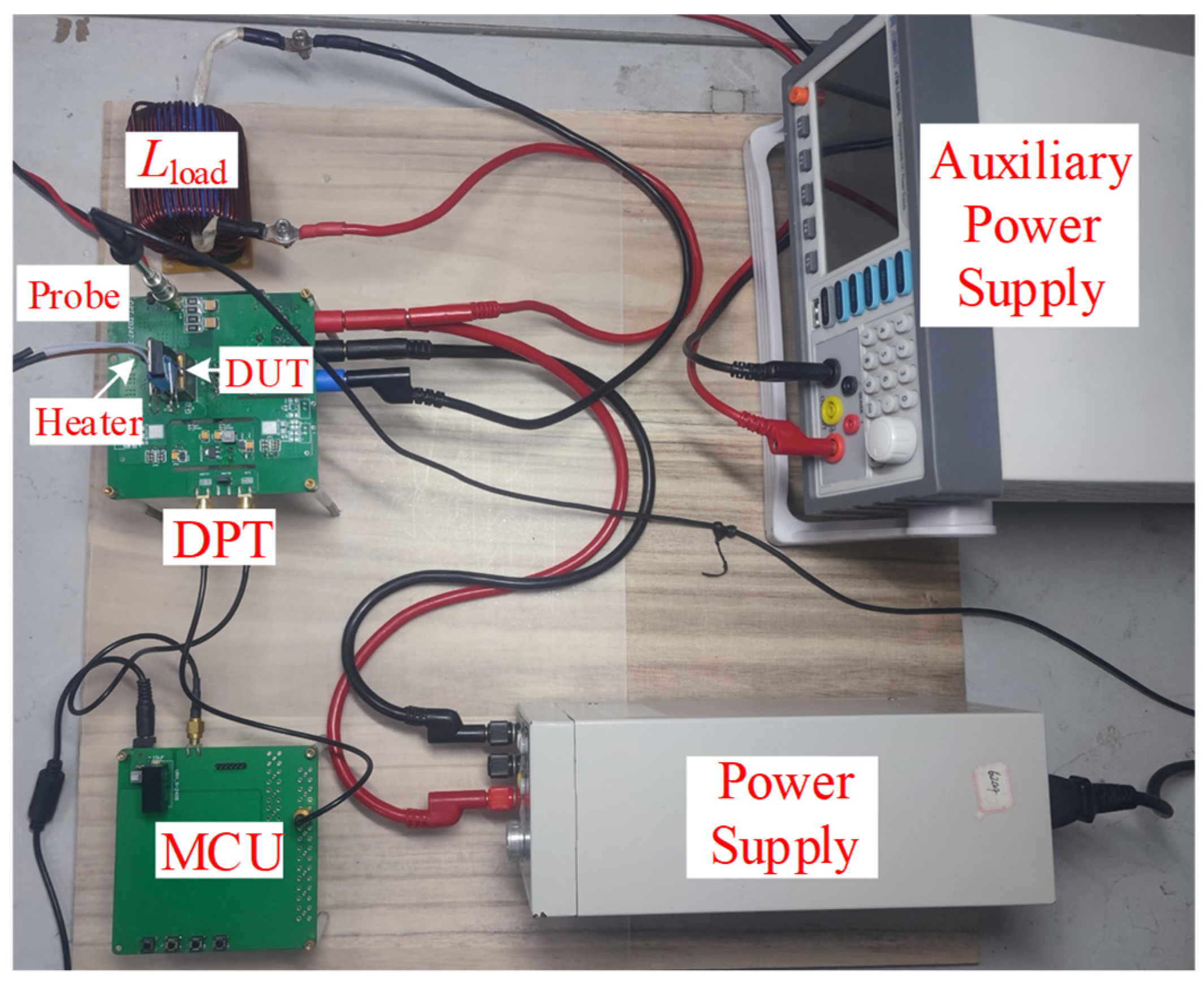
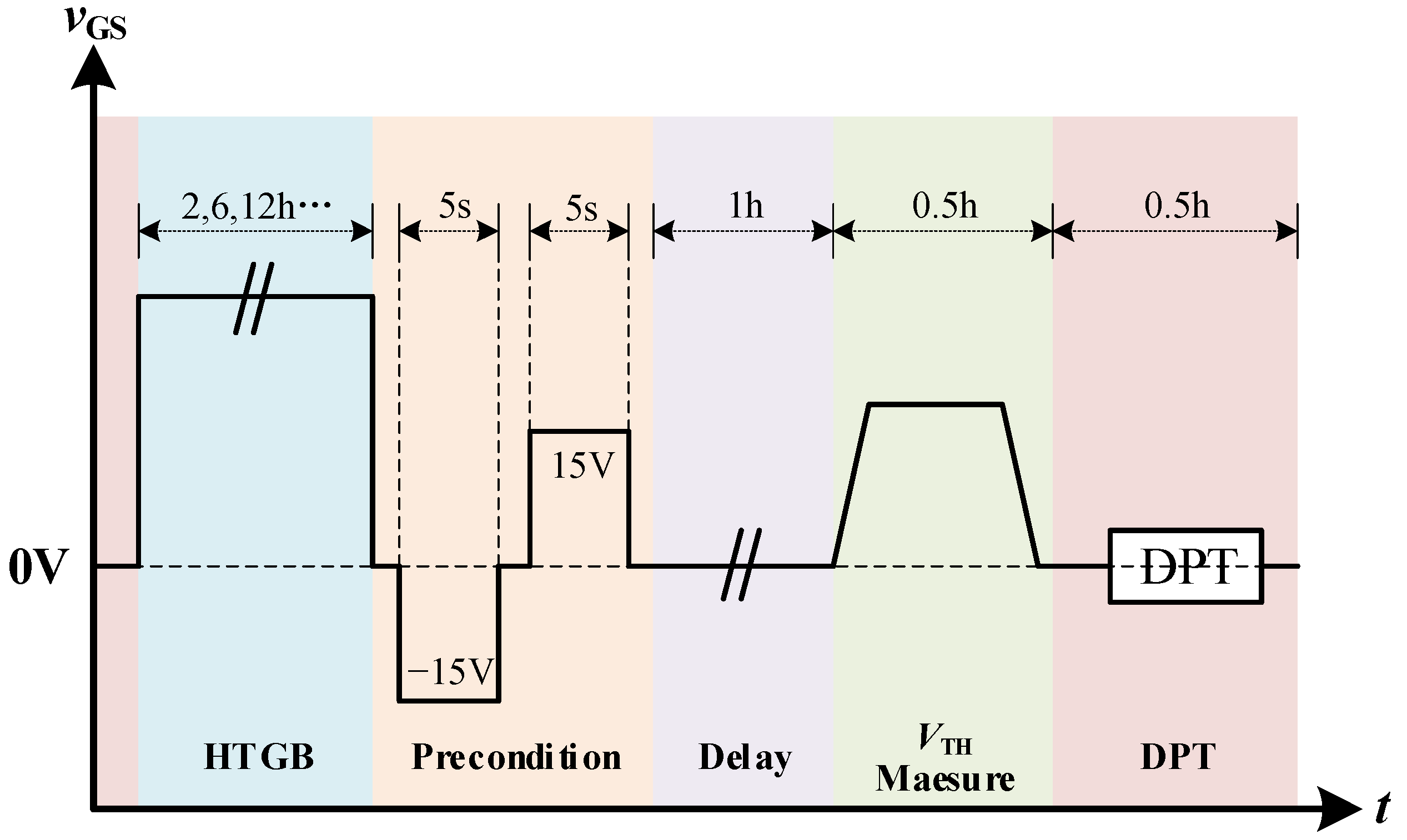
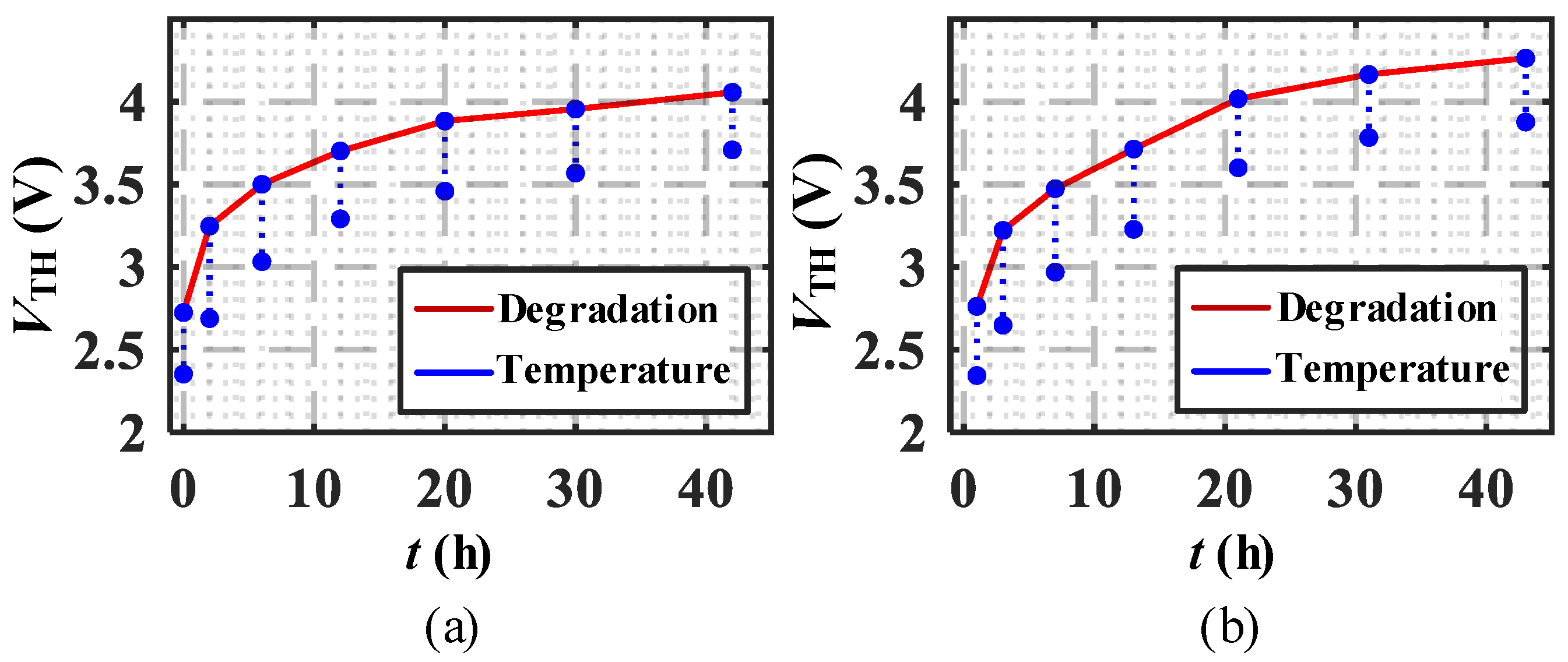
3. Experimental Validation and Analysis

To verify the validity of the proposed method, a discrete SiC MOSFET with a non-Kelvin package (C3M0040120D, 1200 V, 40 mΩ) from CREE has been selected as the device under test (DUT). The vcir_min of the DUT is tested using DPT, which is recognized as an effective method for accurately reproducing the transient behavior of the DUT under the specified voltage and current conditions. The vcir_min is measured with a passive probe with a 500 M bandwidth, as shown in Figure 2. The sampling interface for vcir is positioned between the ends of the path from the source to the negative side of the CDC. The DPT experimental platform is shown in Figure 2. The experimental parameters for the DPT and the specifications of the DUT are shown in Table 1. The Lcir is about 50 nH, which is achieved by finite element simulation. A diDS/dt of 0.2–0.5 A/ns can produce a measurable induction voltage of 10–25 V, demonstrating the feasibility of measuring (diDS/dt)min by circuit parasitic inductance.

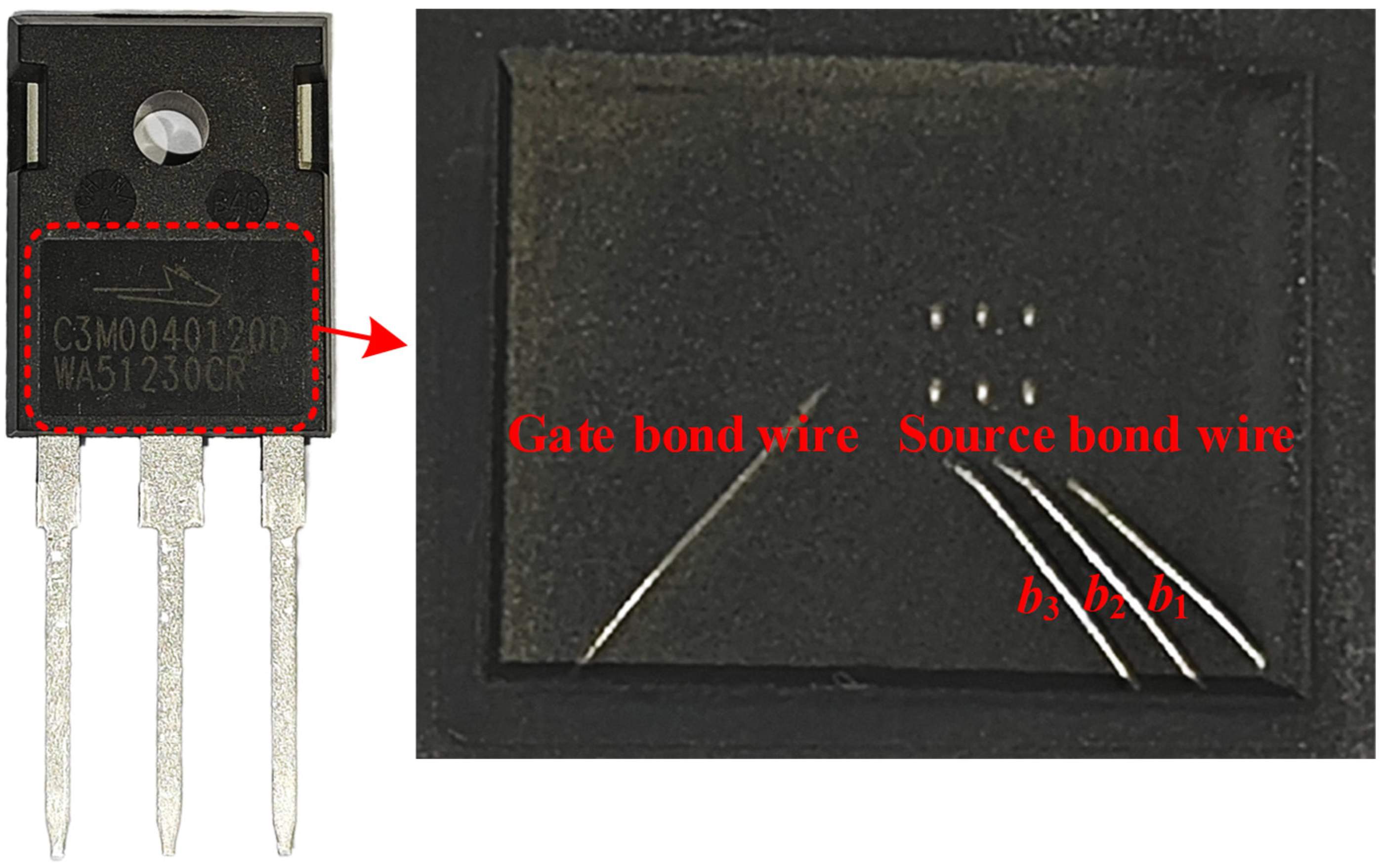
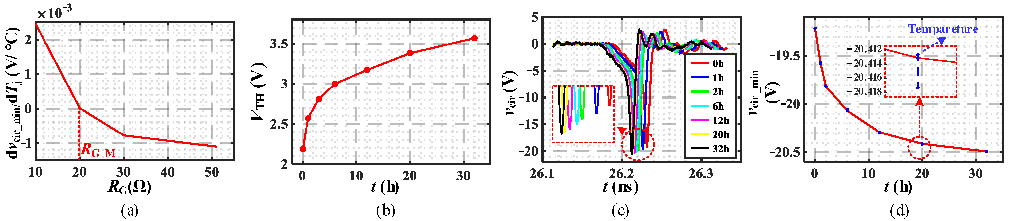
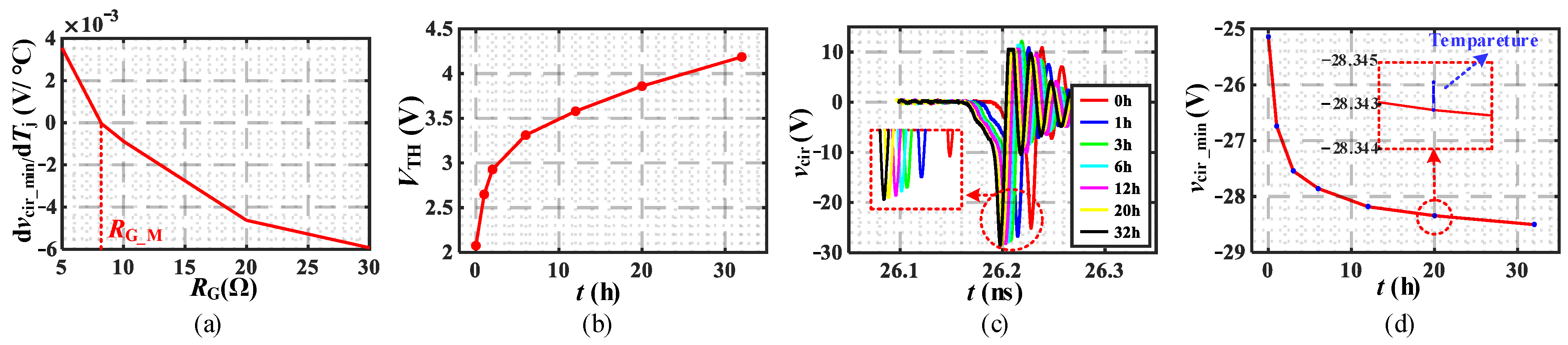
3.1. The Selection of VEE_M and RG_M

The fact that there are two parameters to be determined makes this monitoring method complicated. However, according to (29), the VEE_M as large as possible can meet the monitoring requirements due to the variability among different types of SiC MOSFETs. Furthermore, according to (23) and (28), a smaller VEE_M will be accompanied by a larger RG_M, which could result in |vcir_min| being too small, thereby increasing the difficulty of sampling. Conversely, an excessively large VEE_M may cause the SiC MOSFET gate to break down, while an overly large vcir_min can lead to drain-source overvoltage exceeding design specifications. Therefore, adhering to the maximum negative gate voltage recommended in the datasheet is a prudent choice for VEE_M.
The selection of RG_M should be made after the VEE_M has been established. Computing RG_M directly via (28) is challenging because some parameters cannot be accurately determined. Therefore, it is more sensible to ascertain RG_M by testing the dvcir_min/dTj value with different RG. The VEE_M of the DUT is set to 8 V, and the temperature range for the experiment is established between 25 °C and 150 °C. The case temperature (Tc) of the DUT is regulated by adjusting the output power of the heating plate through a PID controller. To ensure that Tj is approximately equal to Tc during testing, a heating interval of 5 min is selected. Figure 3 shows the mean of dvcir_min/dTj in the range of 25 °C to 150 °C as a function of RG. As shown in Figure 3, the dvcir_min/dTj changes from positive to negative at RG = 24 Ω. Therefore, to eliminate the effect of temperature, the RG_M of this DUT is set to 24 Ω.

3.2. Validation of the Proposed Method

To verify that vcir_min varies with the gate-oxide degradation of SiC MOSFET at VEE_M and RG_M, the degradation of DUT’s gate oxide is accelerated. Subsequently, vcir_min is tested at various degrees of degradation. Several accelerated aging methods can be employed for SiC MOSFETs [2,3,4,5]. By applying constant extreme stress to the gate under high-temperature conditions, the HTGBtest can rapidly reproduce the gate-oxide degradation of SiC MOSFETs. To reduce the experimental duration, a gate voltage of 32 V is applied while the drain of the DUT is shorted to the source. The DUT is maintained at a temperature of 150 °C on a thermostat during the HTGB test. The existing literature has demonstrated that the cumulative trap-capture charge of SiC MOSFETs increases logarithmically with time [12]. Consequently, a gradually increasing test interval is selected. After each HTGB interruption, the DUT must be preconditioned to eliminate the influence of transient changes. The precondition is carried out by applying a negative bias (−15 V) of 5 s and a positive bias (15 V) of 5 s to the gate electrode [30]. Subsequently, the VTH is measured after a delay of 1 h to assess the degree of degradation. The test sequence is shown in Figure 4.
To eliminate serendipity, two DUTs (DUT1 and DUT2) from the same batch are evaluated under identical conditions. The VTH variations over the HTGB test cumulative time and temperature (25–150 °C) are shown in Figure 5, where the results of the DUT2 are shifted forward 1 h for a better presentation, and the interval represented by the blue dotted line indicates the variation of VTH within the temperature range of 25 °C to 150 °C at a given HTGB time. The gate-oxide degradation of the DUT is evidenced by the observed drift of VTH in Figure 5. The quantitative VTH data show that the cumulative HTGB time of 42 h at 32 V gate bias results in a positive VTH shift of 48.88% for DUT1 and 54.38% for DUT2.
The vcir of the DUT2 at different temperatures (25 °C, 70 °C, 110 °C, and 150 °C) are tested in both healthy state and after being stressed for 42 h, and the results are shown in Figure 6. From Figure 6, the vcir_min at different temperatures remains nearly constant in both states, indicating that the dvcir_min/dTj at VEE_M = 8 V and RG_M = 24 Ω is approximately zero and proving the correctness of the theoretical analysis. The variation of vcir of DUT1 with HTGB time for VEE_M = 8 V and RG_M = 24 Ω is shown in Figure 7a. A noticeable decrease in vcir_min is observed during the HTGB test, indicating that the reduction in vcir_min can effectively reflect the degree of the gate-oxide degradation of the DUT. The temperature-induced change of vcir_min from a healthy state to the DUT stressed for 42 h is tested and displayed in Figure 7b, where the results of the DUT2 are shifted forward 0.5 h for a better presentation. The 42 h HTGB time resulted in a 6.55% reduction in vcir_min for DUT1 and a 7.09% reduction for DUT2. The change in vcir_min due to temperature is less than 0.103% throughout the HTGB test. The temperature-induced changes in vcir_min during the HTGB test are significantly smaller than those caused by the gate-oxide degradation of DUT. Therefore, it can be concluded that temperature interference is nearly negligible when using vcir_min at specific RG and VEE to monitor the gate-oxide degradation of SiC MOSFET.

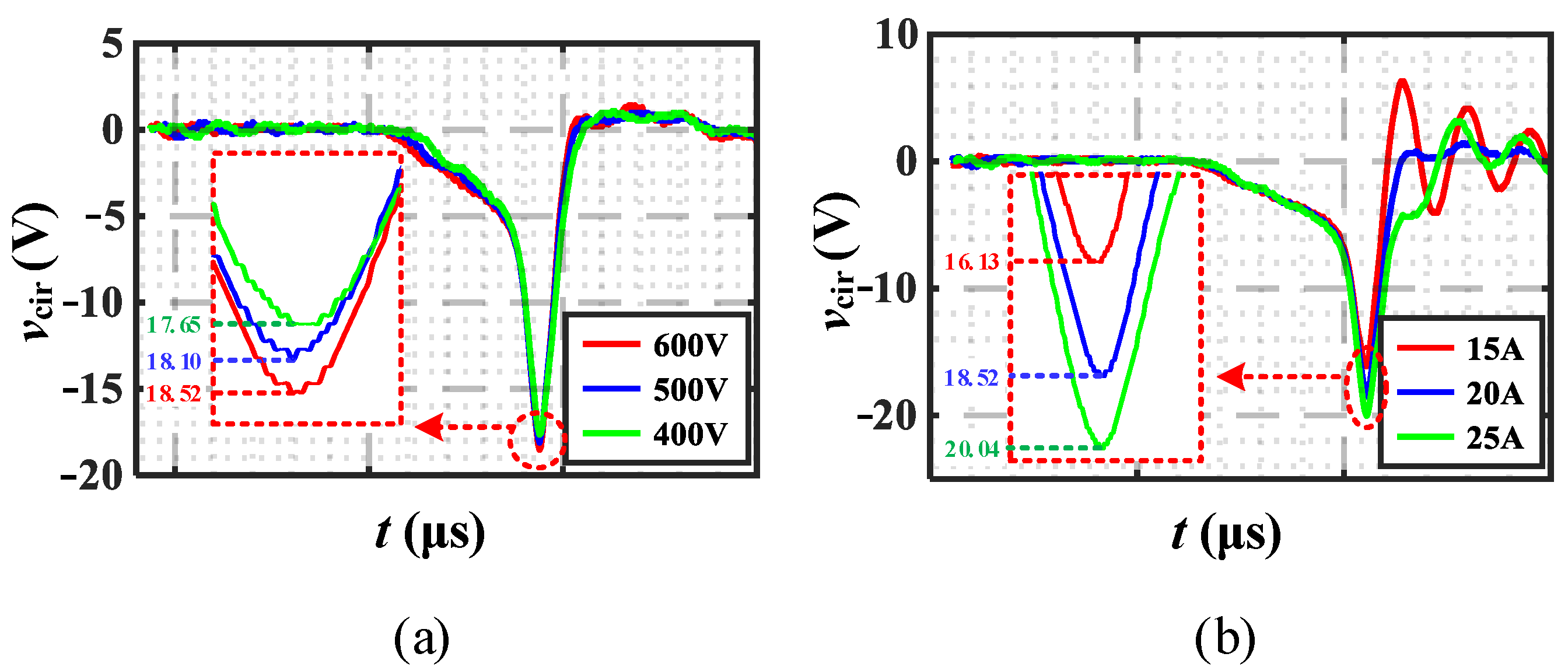
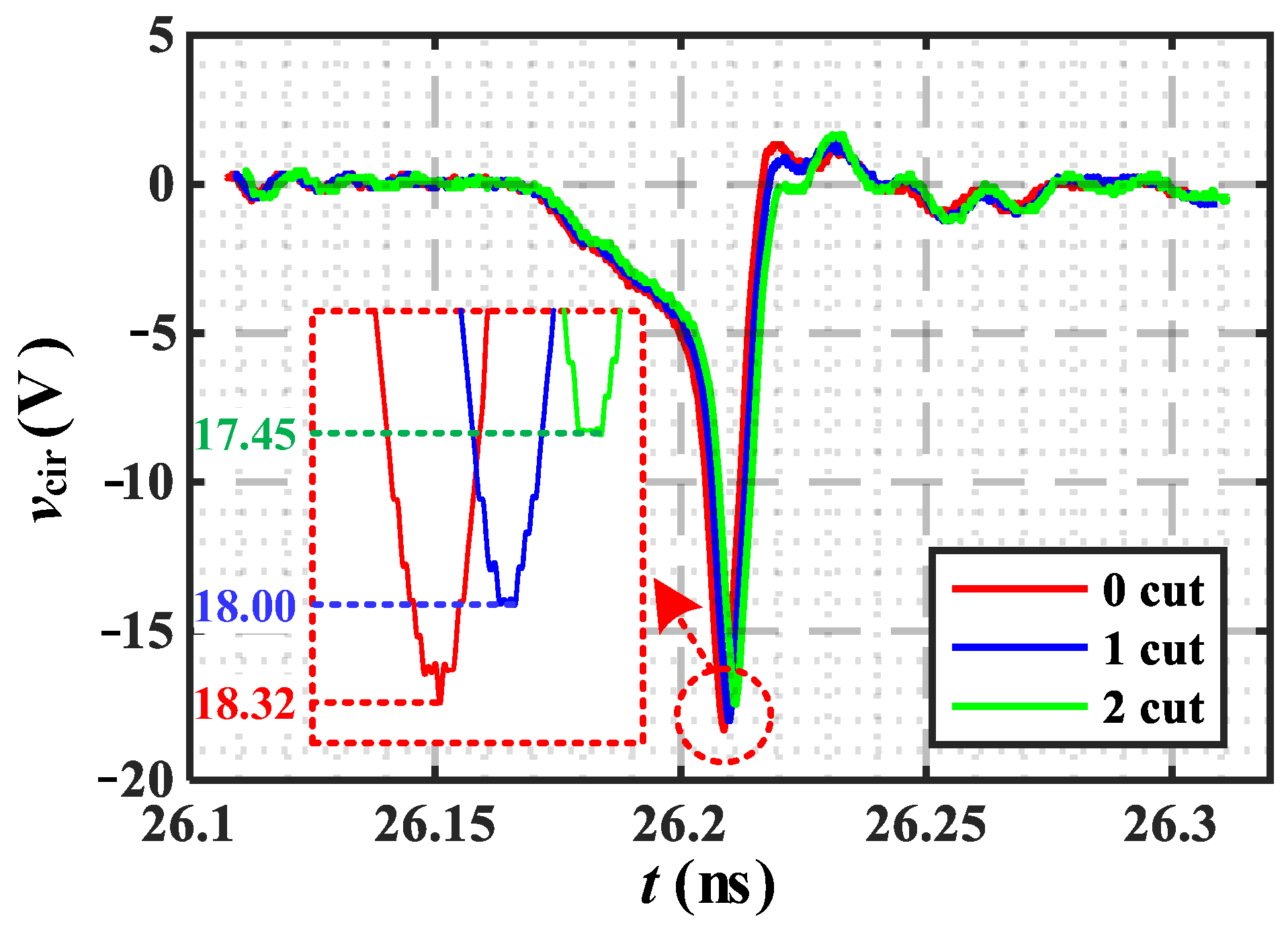
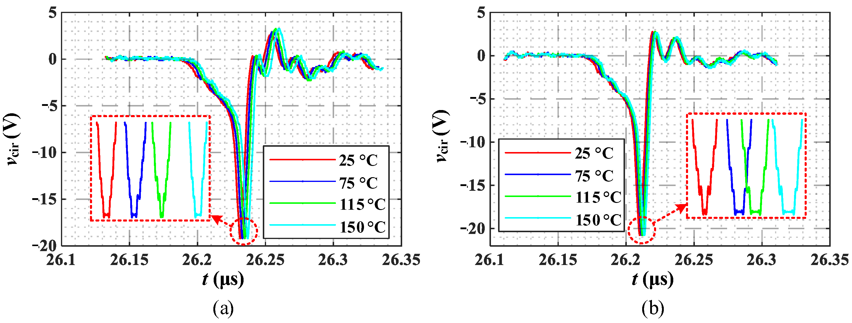
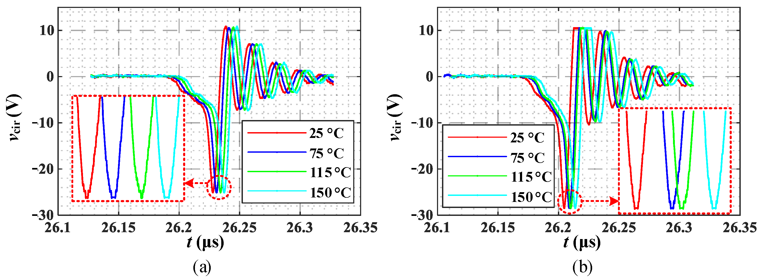
3.3. Affecting Factors of vcir_min

Bus voltage (VDC) fluctuations and load current (Iload) variations may occur in the converter. Therefore, it is essential to evaluate the influence of the VDC and Iload on the vcir_min at VEE_M and RG_M. Figure 8a,b show the vcir_min of a C3M0040120D measured at different VDC and Iload, respectively. According to Figure 8, an increase of 4.70% of vcir_min is observed when VDC is reduced from 600 V to 400 V, while an increase of 19.5% of vcir_min is observed when Iload is reduced from 25 A to 15 A. Compared to the 7% reduction in vcir_min caused by the 42 h HTGB time, the changes in vcir_min due to the variations of VDC and Iload cannot be ignored. Therefore, it is suggested that the proposed degradation monitoring precursor in this paper should be measured at a fixed VDC and Iload.
Bond wire failure is also one of the most prominent ways in which power devices degrade [31,32]. As shown in Figure 9, SiC MOSFETs in the TO 247-3 package have gate bond wires and source bond wires. The source bond wires are typically the most susceptible to damage, as the current flowing through the source bond wires is significantly higher than that in the gate bond wire. Failure of the source bond wires will lead to changes in bond wires’ parasitic resistance and inductance [22]. In TO 247-3 package SiC MOSFET, the bond wires’ parasitic resistance and inductance are in LS. According to (10), the value of vcir_min will vary with LS. Therefore, it is essential to assess the impact of bond wire failure on the vcir_min.
The vcir_min of DUT (C3M0040120D) with different degrees of bond wire failure is tested by wire-cutting experiments. As shown in Figure 9, three root source bond wires are observed in C3M0040120D. The vcir_min under healthy state, one wire (b1) cut, and two wires (b1, b2) cut is tested separately and displayed in Figure 10. The vcir_min in one-wire-cut and two-wire-cut states decreased by 1.75% and 4.75%, respectively, compared to the vcir_min in the healthy state. Therefore, bond wire failure can cause non-negligible interference with the vcir_min used for the gate-oxide degradation monitoring of the TO 247-3 package.
As a result, calibration is required if vcir_min continues to be used to monitor the gate-oxide degradation of the TO 247-3 package after bond wires failure.
Fortunately, SiC MOSFETs with the Kelvin package are becoming increasingly popular due to better dynamic performance. For this type of package, the bond wires’ parasitic inductance is not in LS, meaning that the bond wires’ failure will not affect the vcir_min. Therefore, vcir_min used to monitor the gate-oxide degradation of SiC MOSFETs in packages with Kelvin source will not be influenced by bond wires failure.
Due to the parasitic parameters, undershoot or overshoot is caused by diDS/dt in the VDC and vDS as the SiC MOSFET turns on or off. Snubbers, which are applied to suppress voltage overshoot, would also have an effect on the proposed precursor vcir_min [33]. However, when the buffer is applied, the conclusion that the DC BUS undershoot can still be used to measure junction temperature is presented in [20]. Therefore, it is believed that the application of snubbers does not invalidate the ability of diDS/dt to measure junction temperature or monitor gate-oxide degradation. Otherwise, the parasitic parameters do not vary with temperature or gate-oxide degradation. Thus, the proposed monitoring method can be applied to various circuit designs.

4. Discussion

4.1. Universality Analysis

To verify the universality of the proposed method to SiC MOSFETs, the vcir_min is tested in two other types of SiC MOSFET (DUT3: C3M0032120D, 1200 V, 32 mΩ and DUT4: C3M0021120D, 1200 V, 21 mΩ). Both DUTs have a −8 V gate voltage limit in the datasheet, so the VEE_M is still set to 8 V. The test results for DUT3 and DUT4 are presented in Figure 11 and Figure 12, respectively. The quantitative results are summarized in Table 2.
According to Figure 11a and Figure 12a, both DUT3 and DUT4 have RG_M, which makes dvcir_min/dTj = 0 at VEE_M = 8 V. Different RG_M of DUT3 and DUT4 is observed due to device variability. According to Figure 11c and Figure 12c, the downward trend with HTGB time is shown in the vcir_min of both SiC MOSFETs at VEE_M and RG_M, similar to DUT1 and DUT2. The variation of vcir of DUT3 and DUT4 with temperature, in healthy and degradation (32 h) states, is shown in Figure 13 and Figure 14, respectively. At different HTGB times, the changes in vcir_min due to temperature (25–150 °C) are much smaller than those due to gate-oxide degradation, as shown in Figure 11d and Figure 12d. At 32 h HTGB time, the Δvcir_min of DUT3 and DUT4 due to temperature is 1.72% and 0.66%, respectively, of Δvcir_min due to degradation. Therefore, it can be concluded that the proposed method for monitoring gate-oxide degradation, which is independent of temperature, can be applied to various types of SiC MOSFETs.

4.2. Comparison with Other Precursors

Some existing degradation monitoring precursors are measured and compared with the proposed method, and the results are shown in Table 3. To illustrate the extent to which the monitoring precursors are influenced by temperature, we define a change ratio (ζ) of degradation to temperature, which can be calculated by
ζ = Δ x degradation Δ x temperature
where Δxdegradation and Δxtemperature are the changes in monitoring precursors due to degradation and temperature, respectively. A larger ζ presents a smaller effect of temperature on the monitoring of the gate-oxide degradation. It can be assumed that the effect of temperature can be neglected if ζ is greater than 10.
As can be seen in Table 3, a significant advantage of the proposed method is its ability to exclude temperature interferences, which is readily observable compared to other existing methods. Furthermore, this proposed method does not require the pins of the devices as the test interface, ensuring minimal invasiveness to the system.
Additionally, the peak detector circuit can simplify the measurement of the proposed method significantly. Other diDS/dt measurement methods, such as PCB Rogowski Coil [23] and differential voltage probe [20], can also be used to meet different system designs. Therefore, the proposed method is particularly appealing for systems that experience significant temperature fluctuations or have a completed power part design. Additionally, the existing use of VDC and Iload sensors can ensure consistent testing conditions under different degradation states.

5. Conclusions

In this paper, a temperature-independent gate-oxide degradation monitoring method for SiC MOSFETs based on the minimum turn-off circuit parasitic inductor voltage vcir_min at a specific gate drive resistor and negative gate voltage is proposed. The relationship between the temperature sensitivity dvcir_min/dTj and the RG, VEE is analyzed. It is found that vcir_min can serve as an easily measurable precursor for monitoring the gate-oxide degradation of SiC MOSFETs without temperature interference under suitable RG and VEE. The rationale for selecting RG and VEE for different SiC MOSFETs is presented. The effectiveness of the proposed method for monitoring gate-oxide degradation is validated using the double-pulse test. Experimental results demonstrate that the vcir_min decreases by at least 6.55% under a threshold voltage drift of 48.88%, with a maximum variation of only 0.103% across a temperature range of 25–150 °C.
According to the experimental results, the variations in bus voltage and load current can influence the proposed monitoring method, so it is suggested that consistency of test conditions should be required. In addition, the experimental results indicate that the proposed monitoring precursor is affected by bond wire failure in non-Kelvin packages but remains unaffected in Kelvin packages.
Moreover, the universality of the proposed method for SiC MOSFETs has been verified. Through comparing with existing monitoring methods, the approach presented in this article demonstrates several advantages, including being temperature-independent, non-invasive, and easy to measure.
Only the offline test results of the proposed method are presented in this article due to time constraints. The proposed precursor sampling method needs to be designed, and its online implementation needs further research. In addition, more SiC MOSFETs from different makers need to be tested to refine the universality analysis. These studies will continue in future research.

Author Contributions

P.S., conceptualization; X.Z. and P.S., methodology; X.Z., K.L. and Q.L., software; X.Z., validation; P.S., formal analysis; X.Z. and P.S., investigation; X.Z., P.S. and L.C., resources; X.Z. and Q.L., data curation; X.Z., writing—original draft preparation; X.Z., P.S. and K.L., writing—review and editing; X.Z. and B.W., visualization; P.S., supervision; P.S. and L.C., project administration; P.S., funding acquisition. All authors have read and agreed to the published version of the manuscript.

Funding

This research was funded by the National Natural Science Foundation of China, grant number U22A20226.

Data Availability Statement

The original contributions presented in the study are included in the article; further inquiries can be directed to the corresponding author.

Conflicts of Interest

The authors declare no conflicts of interest.

References

  1. Millán, J.; Godignon, P.; Perpiñà, X.; Pérez-Tomás, A.; Rebollo, J. A Survey of Wide Bandgap Power Semiconductor Devices. IEEE Trans. Power Electron. 2014, 29, 2155–2163. [Google Scholar]
  2. Li, K.; Sun, P.; He, Z.; Huang, X.; Li, Q.; Chen, L.; Luo, Q.; Du, X. Recovery of Quasi-Permanent Bias Temperature Instability in SiC MOSFETs and Its Physical Mechanism. IEEE J. Emerg. Sel. Top. Power Electron. 2024, 12, 5852–5863. [Google Scholar] [CrossRef]
  3. Li, K.; Sun, P.; Zhou, X.; Chen, L.; Liu, Q. Comprehensive Investigations on Recovery Characteristics of Bias Temperature Instability in Planar and Trench SiC MOSFETs. IEEE J. Emerg. Sel. Top. Power Electron. 2024; early access. [Google Scholar] [CrossRef]
  4. Miki, H.; Sagawa, M.; Mori, Y.; Murata, T.; Kinoshita, K.; Asaka, K.; Oda, T. Accurate screening of defective oxide on SiC using consecutive multiple threshold-voltage measurements. In Proceedings of the 2022 IEEE International Reliability Physics Symposium (IRPS), Dallas, TX, USA, 27–31 March 2022; pp. 8B.2-1–8B.2-7. [Google Scholar]
  5. Barón, K.M.; Sharma, K.; Nitzsche, M.; Kallfass, I. Online Monitoring of Degradation Sensitive Electrical Parameters in Inverter Operation for SiC-MOSFETs. In Proceedings of the 2021 IEEE Applied Power Electronics Conference and Exposition (APEC), Phoenix, AZ, USA, 14–17 June 2021; pp. 1235–1241. [Google Scholar]
  6. Zhang, Q.; Li, W.; Zhang, P. A Decoupled Junction Temperature and Aging Level Evaluating Method for SiC MOSFETs. IEEE J. Emerg. Sel. Top. Power Electron. 2024, 12, 2558–2568. [Google Scholar] [CrossRef]
  7. Jiang, X.; Wang, J.; Yu, H.; Chen, J.; Zeng, Z.; Yang, X.; Shen, Z.J. Online Junction Temperature Measurement for SiC MOSFET Based on Dynamic Threshold Voltage Extraction. IEEE Trans. Power Electron. 2021, 36, 3757–3768. [Google Scholar] [CrossRef]
  8. Farhadi, M.; Vankayalapati, B.T.; Sajadi, R.; Akin, B. AC Power Cycling Test Setup and Condition Monitoring Tools for SiC-Based Traction Inverters. IEEE Trans. Veh. Technol. 2023, 72, 12728–12743. [Google Scholar] [CrossRef]
  9. Pu, S.; Yang, F.; Vankayalapati, B.T.; Ugur, E.; Xu, C.; Akin, B. A Practical On-Board SiC MOSFET Condition Monitoring Technique for Aging Detection. IEEE Trans. Ind. Appl. 2020, 56, 2828–2839. [Google Scholar] [CrossRef]
  10. Ugur, E.; Xu, C.; Yang, F.; Pu, S.; Akin, B. A New Complete Condition Monitoring Method for SiC Power MOSFETs. IEEE Trans. Ind. Electron. 2021, 68, 1654–1664. [Google Scholar] [CrossRef]
  11. Ye, X.; Chen, C.; Wang, Y.; Zhai, G.; Vachtsevanos, G.J. Online Condition Monitoring of Power MOSFET Gate Oxide Degradation Based on Miller Platform Voltage. IEEE Trans. Power Electron. 2017, 32, 4776–4784. [Google Scholar] [CrossRef]
  12. Karki, U.; González-Santini, N.S.; Peng, F.Z. Effect of Gate-Oxide Degradation on Electrical Parameters of Silicon Carbide MOSFETs. IEEE Trans. Electron Devices 2020, 67, 2544–2552. [Google Scholar] [CrossRef]
  13. Ouaida, R.; Berthou, M.; León, J.; Perpina, X.; Oge, S.; Brosselard, P.; Joubert, C. Gate Oxide Degradation of SiC MOSFET in Switching Conditions. IEEE Electron Device Lett. 2014, 35, 1284–1286. [Google Scholar] [CrossRef]
  14. Erturk, F.; Ugur, E.; Olson, J.; Akin, B. Real-Time Aging Detection of SiC MOSFETs. IEEE Trans. Ind. Appl. 2019, 55, 600–609. [Google Scholar] [CrossRef]
  15. Farhadi, M.; Yang, F.; Pu, S.; Vankayalapati, B.T.; Akin, B. Temperature-Independent Gate-Oxide Degradation Monitoring of SiC MOSFETs Based on Junction Capacitances. IEEE Trans. Power Electron. 2021, 36, 8308–8324. [Google Scholar] [CrossRef]
  16. Xie, M.; Sun, P.; Wang, K.; Luo, Q.; Du, X. Online Gate-Oxide Degradation Monitoring of Planar SiC MOSFETs Based on Gate Charge Time. IEEE Trans. Power Electron. 2022, 37, 7333–7343. [Google Scholar] [CrossRef]
  17. Zhang, W.; Qi, L.; Tan, K.; Ji, B.; Zhang, X.; Chai, W.; Cui, X. IGBT Junction Temperature Estimation Using a Dynamic TSEP Independent of Wire Bond Faults. IEEE Trans. Power Electron. 2023, 38, 5323–5334. [Google Scholar] [CrossRef]
  18. Fang, X.; Sun, P.; Wang, B.; Luo, Q.; Du, X. Online Bridge-Level Junction Temperature Evaluation of IGBTs via Emitter Parasitic Inductance Voltage Undershoot. IEEE Trans. Ind. Electron. 2024, 71, 16728–16738. [Google Scholar] [CrossRef]
  19. Yang, Y.; Zhang, P. In Situ Insulated Gate Bipolar Transistor Junction Temperature Estimation Method via a Bond Wire Degradation Independent Parameter Turn-OFF Vce Overshoot. IEEE Trans. Ind. Electron. 2021, 68, 10118–10129. [Google Scholar] [CrossRef]
  20. Yang, Y.; Wu, Y.; Ding, X.; Zhang, P. Online Junction Temperature Estimation Method for SiC MOSFETs Based on the DC Bus Voltage Undershoot. IEEE Trans. Power Electron. 2023, 38, 5422–5431. [Google Scholar] [CrossRef]
  21. Fang, X.; Sun, P.; He, C.; Wang, B. Online Converter-level Temperature Estimation for IGBTs Using Proportional Calibration Method. IEEE Trans. Power Electron. 2024, 40, 157–161. [Google Scholar] [CrossRef]
  22. Xie, M.; Sun, P.; Ouyang, W.; Luo, Q.; Du, X. Online Monitoring Bond Wires Fault of SiC MOSFETs With Kelvin Package Based on Turn-on Source Voltage Ringing. IEEE Trans. Ind. Electron. 2024, 71, 9767–9776. [Google Scholar] [CrossRef]
  23. Kang, J.; Zhu, A.; Chen, Y.; Luo, H.; Yao, L.; Xin, Z. An Online Gate Oxide Degradation Monitoring Method for SiC MOSFETs With Contactless PCB Rogowski Coil Approach. IEEE Trans. Power Electron. 2023, 38, 9673–9684. [Google Scholar] [CrossRef]
  24. Jahdi, S.; Alatise, O.; Alexakis, P.; Ran, L.; Mawby, P. The Impact of Temperature and Switching Rate on the Dynamic Characteristics of Silicon Carbide Schottky Barrier Diodes and MOSFETs. IEEE Trans. Ind. Electron. 2015, 62, 163–171. [Google Scholar] [CrossRef]
  25. Pérez-Tomás, A.; Brosselard, P.; Godignon, P.; Millán, J.; Mestres, N.; Jennings, M.R.; Covington, J.A.; Mawby, P.A. Field-effect mobility temperature modeling of 4H-SiC metal-oxide-semiconductor transistors. J. Appl. Phys. 2006, 100, 114508. [Google Scholar] [CrossRef]
  26. Yang, L.; Bai, Y.; Li, C.; Chen, H.; Han, Z.; Tang, Y.; Hao, J.; Yang, C.; Tian, X.; Lu, J.; et al. Analysis of Mobility for 4H-SiC N/P-Channel MOSFETs Up To 300 °C. IEEE Trans. Electron Devices 2021, 68, 3936–3941. [Google Scholar] [CrossRef]
  27. Sun, P.; Guo, Y.; Wu, T.; Zhao, Z.; Lai, P.; Chen, Z.; Qi, L.; Cui, X. An Online Junction Temperature Monitoring Correction Method for SiC MOSFETs at Different Parasitic Parameters. IEEE J. Emerg. Sel. Top. Power Electron. 2022, 10, 5007–5018. [Google Scholar] [CrossRef]
  28. González, J.A.O.; Alatise, O. A Novel Non-Intrusive Technique for BTI Characterization in SiC mosfets. IEEE Trans. Power Electron. 2019, 34, 5737–5747. [Google Scholar] [CrossRef]
  29. Wang, M.; Zhang, J.; Ng, W.T.; Nishio, H.; Iwamoto, M.; Sumida, H. Application of a Smart Gate Driver to Detect Aging in SiC Power MOSFETs. In Proceedings of the 2023 35th International Symposium on Power Semiconductor Devices and ICs (ISPSD), Hong Kong, China, 28 May–1 June 2023; pp. 187–190. [Google Scholar]
  30. Zhong, X.; Jiang, H.; Qiu, G.; Tang, L.; Mao, H.; Xu, C.; Jiang, X.; Hu, J.; Qi, X.; Ran, L. Bias Temperature Instability of Silicon Carbide Power MOSFET Under AC Gate Stresses. IEEE Trans. Power Electron. 2022, 37, 1998–2008. [Google Scholar] [CrossRef]
  31. Zhang, J.; Shen, H.; Du, X.; Chen, R. Condition Monitoring the Inhomogeneous Thermal Fatigue of Multichip IGBT Module Based on the Thermal Attenuation Coefficient. IEEE Trans. Power Electron. 2025, 40, 2114–2125. [Google Scholar] [CrossRef]
  32. Zhao, S.; Yang, X.; Wu, X.; Liu, G. Investigation on Creep-Fatigue Interaction Failure of Die-Attach Solder layers in IGBTs Under Power Cycling. IEEE Trans. Power Electron. 2025; early access. [Google Scholar] [CrossRef]
  33. Xu, M.; Yang, X.; Li, J. C-RC Snubber Optimization Design for Improving Switching Characteristics of SiC MOSFET. IEEE Trans. Power Electron. 2022, 37, 12005–12016. [Google Scholar] [CrossRef]
Figure 1. The vcir at turn-off. (a) Schematic circuit. (b) Typical turn-off process of SiC MOSFET.
Electronics 14 00771 g001
Figure 2. DPT platform.
Electronics 14 00771 g002
Figure 3. dvcir_min/dTj of DUT as a function of RG at turn-off (@VDC = 600 V, Iload = 20 A, VEE_M = 8 V, Tj = 25 °C).
Electronics 14 00771 g003
Figure 4. Experimental sequence.
Electronics 14 00771 g004
Figure 5. The VTH of DUT drift with HTGB time and temperature. (a) DUT1. (b) DUT2 (25–150 °C) (@iDS = 5 mA, vGS = vDS).
Electronics 14 00771 g005
Figure 6. The variation of vcir with temperature (25–150 °C) at healthy state and degradation state. (a) Healthy state. (b) State after 32 V stressed for 42 h (@VDC = 600 V, Iload = 20 A, VEE_M = 8 V, RG_M = 24 Ω).
Electronics 14 00771 g006
Figure 7. The variation of vcir with HTGB time and temperature (25–150 °C). (a) The variation of vcir (@Tj = 25 °C). (b) The variation of vcir_min (@VDC = 600 V, Iload = 20 A, VEE_M = 8 V, RG_M = 24 Ω).
Electronics 14 00771 g007
Figure 8. The variation of vcir_min at different VDC and Iload. (a) Different VDC (@Iload = 20 A). (b) Different Iload (@VDC = 600 V) (@Tj = 25 °C).
Electronics 14 00771 g008
Figure 9. Bond wires in C3M0040120D.
Electronics 14 00771 g009
Figure 10. The variation of vcir_min in SiC MOSFETs with non-Kelvin package at different number bond wires cut (@VDC = 600 V, Iload = 20 A, Tj = 25 °C).
Electronics 14 00771 g010
Figure 11. Experiment results of the DUT3. (a) dvcir_min/dTj of DUT3 as a function of RG for VEE_M = 8 V at turn-off. (b) The VTH of DUT drift with HTGB time (@iDS = 5 mA, vGS = vDS). (c) The variation of vcir with HTGB time (@Tj = 25 °C). (d) The variation of vcir_min with HTGB time and temperature (25–150 °C) (@VDC = 600 V, Iload = 20 A, VEE_M = 8 V, RG_M = 20 Ω).
Electronics 14 00771 g011
Figure 12. Experiment results of the DUT4. (a) dvcir_min/dTj of DUT3 as a function of RG for VEE_M = 8 V at turn-off. (b) The VTH of DUT drift with HTGB time (@iDS = 5 mA, vGS = vDS). (c) The variation of vcir with HTGB time (@Tj = 25 °C). (d) The variation of vcir_min with HTGB time and temperature (25–150 °C) (@VDC = 600 V, Iload = 20 A, VEE_M = 8 V, RG_M = 8.2 Ω).
Electronics 14 00771 g012
Figure 13. The variation of vcir of DUT3 with temperature (25–150 °C) at healthy state and degradation state. (a) Healthy state. (b) State after 32 V stressed for 32 h (@VDC = 600 V, Iload = 20 A, VEE_M = 8 V, RG_M = 20 Ω).
Electronics 14 00771 g013
Figure 14. The variation of vcir of DUT4 with temperature (25–150 °C) at healthy state and degradation state. (a) Healthy state. (b) State after 32 V stressed for 32 h (@VDC = 600 V, Iload = 20 A, VEE_M = 8 V, RG_M = 8.2 Ω).
Electronics 14 00771 g014
Table 1. Experimental parameters.
ParameterValueParameterValue
VDC600 VVGH15 V
Iload20 ALload700 μH
Rated voltage1200 VRated current66 A
Max VGH/VEE19/−8 VRef VGH/VEE15/−4 V
Table 2. Experimental parameter test results of DUT3 and DUT4.
ParameterValueParameterValue
VEE_M (V)8VEE_M (V)8
RG_M (Ω)20RG_M (Ω)8.2
ΔVTH/VTH_healthy63.01%ΔVTH/VTH_healthy91.27%
Δvcir_min/vcir_min_healthy6.64%Δvcir_min/vcir_min_healthy13.38%
Δvcir_min/vcir_min_25 °C0.114%Δvcir_min/vcir_min_25 °C0.089%
Table 3. Comparison with different methods.
Test
Condition
Monitoring
Precursors
Degradation
Value
Temperature
Value
Degradation
Sensitivity
ζVDCIloadBond Wires
Failure
Test
Interface
150   ° C ,   32   V   for   42   h 25 150   ° C vcir_min1.302 V0.019 V7.09%68.8yesyesyes for non-Kelvin
no for Kelvin
BUS
VTH (5 mA)1.501 V0.251 V54.38%5.99nononoG, S
RON (20 A, 15 V)7.4 mΩ19.5 mΩ13.8%0.39noyesyesD, S
VSD (20 A, −4 V)0.198 V0.450 V4.22%0.44noyesyesD, S
Igss (15 V)200 pA<40 pA<500 pA×nononoG
Disclaimer/Publisher’s Note: The statements, opinions and data contained in all publications are solely those of the individual author(s) and contributor(s) and not of MDPI and/or the editor(s). MDPI and/or the editor(s) disclaim responsibility for any injury to people or property resulting from any ideas, methods, instructions or products referred to in the content.

