1. Introduction
Nowadays, the developments of remote and contactless sensors have propelled the progress of wireless sensing technologies, bringing wireless sensors with diversified frameworks and functionalities [
1,
2]. Different from the wired sensor, with evident drawbacks in terms of the must-have battery on board that always occupies a large area and is difficult to conduct maintenance and battery replacement, the wireless sensor is free of this constraint, revealing more appropriative for long-term or even eternal deployment, especially inside the danger and hazard environment [
3]. In addition, compared with the active sensors that have to be equipped with integrated circuits (ICs), the passive sensors possess some IC functions that do not need onboard battery or wireless power transfer units to be effective in avoiding the necessity of periodic battery renewing in real-time and real-field monitoring or sensing applications [
4,
5,
6]. On this account, the fundamental topology of a passive wireless sensor system is composed of several passive sensors with one interrogator. The process of interrogation is based on the mechanism of backscatter communication. The interrogator disseminates electromagnetic waves as interrogating signals, impinging on sensors and bouncing backward. The interrogator can then receive these backscattered signals, conducting reading and identification based on the principle that the sensed information will be endorsed with distinguished signatures in different formats or schemes of modulation [
7].
Up to now, passive wireless sensor technology and related application scenarios have attracted a lot of attention from both research and commercial sectors. With the progress of modern microelectromechanical systems (MEMS) and integrated circuit technology, the passive wireless sensors can be innovatively configured to make it more appropriative for applications that utterly require constraint size, dimension, and power consumption, along with simpler architecture, wider environmental suitability, lower cost, and easier utilization, etc. [
8]. However, passive wireless sensors have inherent disadvantages, mainly concerning comparatively lower information capacity, that need to be overcome completely [
9,
10].
Therefore, in this paper, an enhanced multi-bit passive wireless sensor based on UWB spectral–temporal joint coding and modulation is designed and developed based on the uniqueness of UWB’s super-narrow electromagnetic pulse. The proposed sensor has such novelty feature: (1) the sensor unit is a planar patch structure covering the UWB standardized bandwidth ranged from 3.1 GHz to 10.6 GHz; (2) the patch structure is etched by a U-slot that can bring about band gaps in the specific frequency domain; (3) the patch structure is fed by a meander microstrip line that can bring about exact narrow pulse in the time domain; (4) a sensor node is embedded and located in the middle of the U-slot and the node’s status quo and the length of U-slot collaborate to issue modulation upon the band gap to realize the digital code in the frequency domain; (5) a sensor node is equipped at the terminal of the meander microstrip line, whose status quo and the length of the meander line cooperate to issue modulation upon the pulse’s amplitude to realize the digital code in the time domain; (6) four such kind of sensor units with different length of U-slot and different meander microstrip line are combined cubically to configure the sensor’s architecture with digital capacity up to eight bits. The novelty of the proposed sensor is that the uniqueness of such a passive and battery-free sensing structure is able to create distinguished structural mode and antenna mode in the backscattered pulse, exhibiting the characteristics of ultra-wide bandwidth and ultra-short pulse, respectively. The combination of such sensor units can realize simultaneous spectral–temporal joint coding with enhanced capacity of multi-bits.
The paper is organized as follows:
Section 2 introduces the theoretical model of UWB technology governing passive sensor nodes that are chipless or battery-free;
Section 3 describes the architecture of the sensor unit;
Section 4 issues the sensor that is endorsed with signatures typically in spectral–temporal joint coding and modulation;
Section 5 introduces the prototype of the sensor with enhanced capacity of multi-bits;
Section 6 fabricates the sensor and verifies it by results and discussion; and
Section 7 gives the conclusion.
2. Theoretical Model
The UWB technology is a formula used specifically for short-range wireless communication that, when an extremely wide band is employed, shows many outstanding features such as low spectrum occupation, low power consumption, and strong anti-interference. In commercial use, the frequency band ranging from 3.1 GHz to 10.6 GHz is specifically allocated for promoting short-range communication with large capacity [
11]. In principle, what we call the UWB has two deterministic definitions. The first is the relative bandwidth that is equal to or greater than 20%, as shown in Equation (1).
The second is the absolute bandwidth, denoting bandwidth exceeding 500 MHz, as shown in Equation (2).
where
,
and
represent the lowest, the highest, and the center frequency, respectively [
12].
Accordingly, in the time domain, the UWB signal is a very short pulse shortened by approximating the nanosecond level between 0.2 and 1.5 ns. Since it is very short in the time domain whilst having a high-tier temporal resolution, the UWB system is able to adopt a periodic pulse to carry and transmit data with a low-duty cycle that, as a result, can reduce power consumption greatly. Moreover, due to the extremely narrow pulse, the multipath effect is not very easy to overlap in the time axial, which can enable a receiver to have the capability to separate multipath signals effectively to improve the resolution of multipath effects [
13].
On the contrary, in the frequency domain, the bandwidth of the UWB spectrum can be awfully extended to an extremely high energy dispersion, and since it has a relatively lower power spectral density, the UWB can enable the interference interfering with other wireless systems to be minimum to improve the spectral efficiency of utilization [
14,
15].
Therefore, the UWB system is regarded as the optimal architecture for a wireless sensor system that is usually equipped with passive sensor nodes that are chipless or battery-free [
16]. Upon the issue of both the research and the application, the small size, low profile, and high-efficiency passive sensor topology is always the hot subject. For example, the UWB is applied to a printed microstrip antenna with an etched ground plane to extend its operating frequency, covering the overall UWB band [
17]. It can also be applied to a compact UWB printed monopole antenna with higher gain and efficiency that is light-weight, low-cost, easy to manufacture, and better integrating with other systems to provide the solution for short-range communication with large capacity and traffic [
18].
3. Sensor Unit
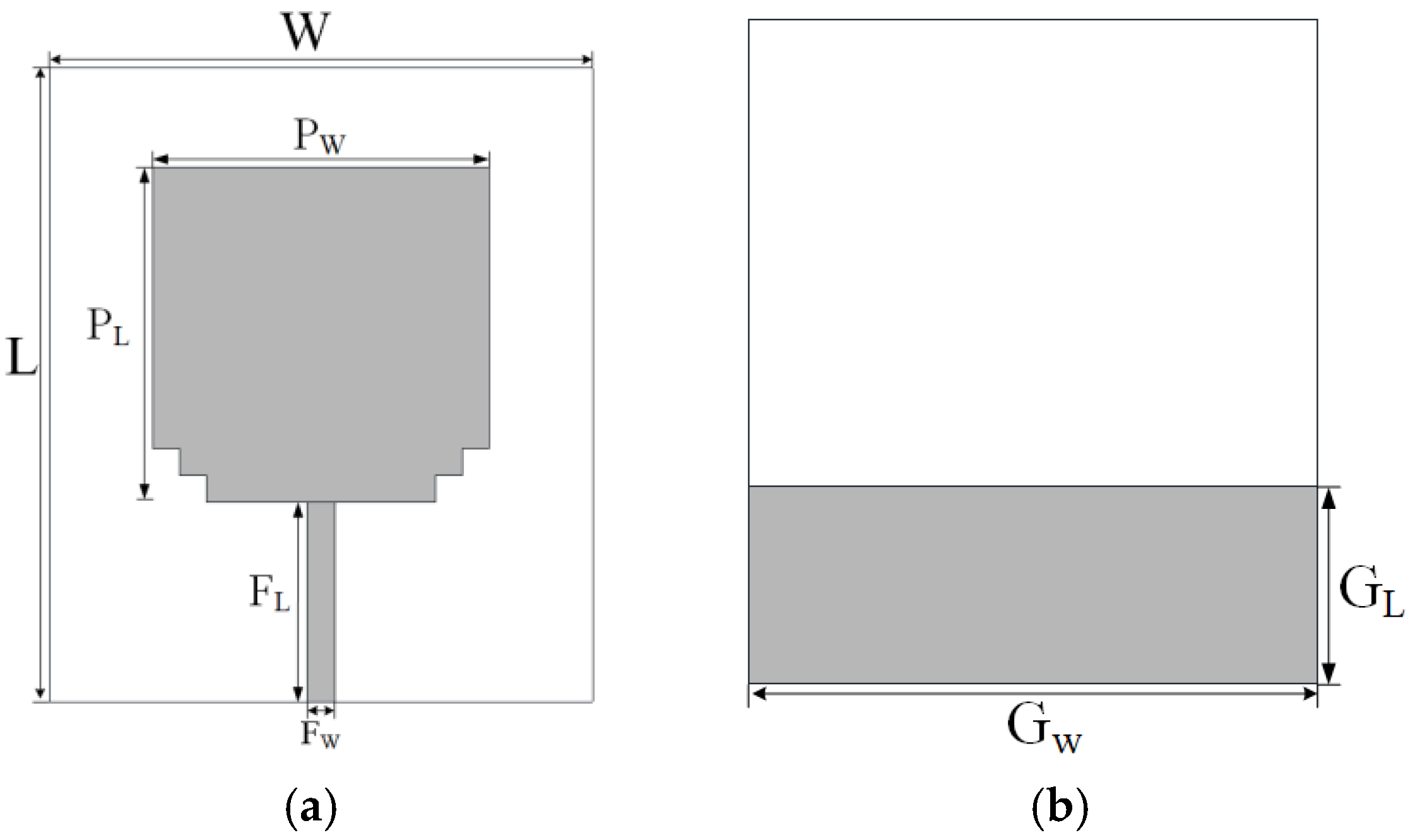
The sensor unit is designed as shown in
Figure 1. It is illustrated by a metallic planar patch printed on the surface of the PCB board fed by a microstrip line with a grounding plane printed on the bottom side. The PCB board is the RF4 type with a dielectric constant of 2.33. The size of the sensor unit is 30 mm long (W), 35 mm wide (L), and 0.5 mm thick (H). The size of the metallic patch is 18.6 mm long (P
W) and 18.5 mm wide (P
L). The two bottom edges are specifically designed with two-level staircases in order to widen the bandwidth as much as possible. The metallic patch is fed by a microstrip line that is 11 mm in length (F
L) and 1.5 mm in width (F
W), as shown in
Figure 1a. As a microstrip line, the grounding plate is 30 mm in length (G
W) and 10.4 mm in width (G
L), which is printed on the bottom side of the PCB board, as shown in
Figure 1b.
Simulation is implemented by CST microwave studio, and the parameters of the structural model are determined, as shown in
Figure 1. Simulation is conducted to verify the performance of the proposed sensor unit. As shown in
Figure 2, the S11 parameter is achieved by lowering the threshold level by −10 dB, which can consistently cover the entire bandwidth of UWB ranging from 3.1 GHz to 10.6 GHz. The results show that the sensor unit is a qualified architecture working well in the UWB band.
3.1. Sensor Unit with Frequency Domain Coding and Modulation
The ultra-wideband characteristic of the sensor unit can also provide a large span of spectra that makes it possible to be manipulated by sensed information in more possible ways. One effective method is to bring about band gap phenomena in the assigned frequency slot and the magnitude, compared with the threshold level, which is a distinguished signature that can be modulated and coded by digits.
For that, a U-slot is etched on the metallic patch, as shown in
Figure 3, in which
Figure 3a is the case that the sensor is not equipped with the sensor head, and
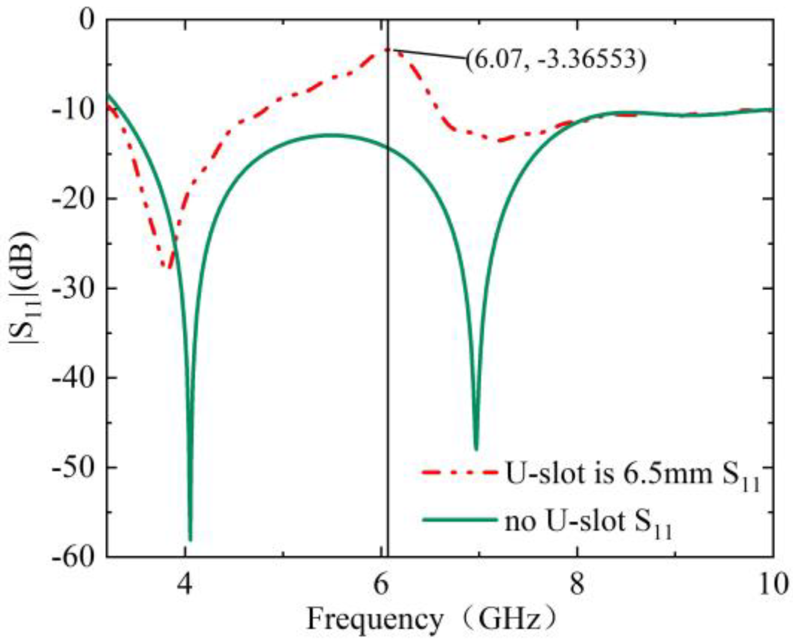
Figure 3b is the reverse case where the sensor is equipped with the sensor head. The sensor head functions as the open denoted by red dot curve or short denoted by green solid curve, which is used to modulate the signature in the frequency domain coded with digital bit 1 or 0. When the length of the U-slot is 6.5 mm, the study shows that there is a band gap at the frequency slot of 6.07 GHz, as shown in
Figure 4.
This result indicates that the behavior of the sensor unit can be reconfigured by a U-slot; that is, if there is a U-slot, there must be a band gap in this assigned frequency slot. Conversely, if there is not a U-slot, there will not be a band gap. Therefore, the band gap frequency slot can be set as the sensor’s signature modulated in the frequency domain by the U-slot or coded with digital bit 1 or 0.
The simulation also shows that when the U-slot is shortened, the band gap at the assigned frequency slot will disappear, as shown in
Figure 5.
Therefore, if the U-slot is manipulated by a sensor head that functions as a diode performance along with the variation in the information aimed for sensing, the sensor unit can be borne with the sensed information at the frequency domain in the assigned band gap. If the threshold level of S11 is set by −10 dB, the sensed information can be determined by digital bit 1/0. For example, 1 denotes that the U-slot existed, and 0 denotes that there is no U-slot.
3.2. Sensor Unit with Time Domain Coding and Modulation
The ultra-wideband characteristic of the sensor unit, as shown in
Figure 1, can provide a very short pulse in the time domain that can be manipulated by the information undergone sensing and sensation. One effective way is to bring about a microstrip line with length at an assigned time slot, and the magnitude of the pulse is an ostensive signature that can be modulated in the time axial.
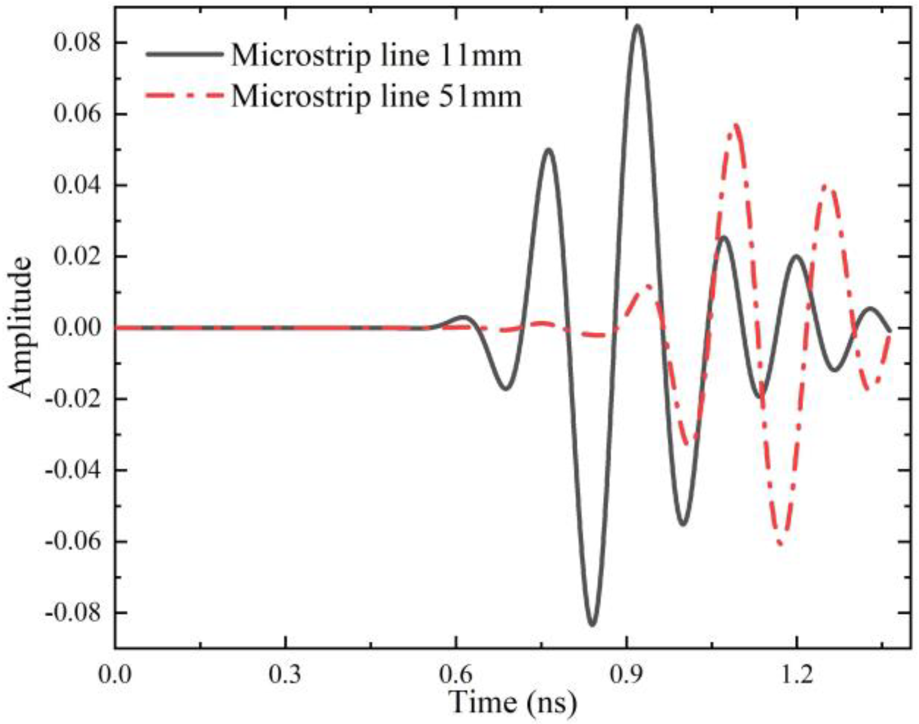
Hence, a meander line is specified as the microstrip line, as shown in
Figure 6. When the total length of the meander microstrip line is 11 mm, the pulse will appear at nearly 0.6 ns in the time axial. When the total length of the meander microstrip line is extended to 51 mm, the pulse, reversed due to being reflected by the short end at the terminal of the microstrip line, will appear at 0.9 ns in the time axial, as shown in
Figure 7.
The result shows that the pulse reflected by the sensor unit has two highlighted signatures used to carry the sensed information. One is the time slot at which the reflected pulse appears in the time axial determined by the length of the meander microstrip line; the other is the amplitude and the phase of the reflected pulse compared with the amplitude and the phase of the pulse disseminated by the interrogator. If the terminal of the meander microstrip line is equipped with an open end, the phase of the pulse is 0 degrees; in contrast, if the terminal of the meander microstrip line is equipped with a short end, the phase of the pulse is reverse to be 180 degrees; and if the terminal is impedance matching to the impedance of the meander microstrip line, the amplitude of the pulse, in theory, is 0, as shown in
Figure 8.
4. Sensor with Spectral–Temporal Joint Coding and Modulation
As discussed above, it is concluded that by etching different lengths of the U slot on the sensor unit, the band gap’s characteristic can be obtained at different frequency slots that render it to bear with different sensed information. The capacity of the sensed information can then be increased, known as spectral modulation or spectral coding, in a digital way. Simulation shows that the longer the length of the U-slot is, the lower the band gap frequency slot will be. Thus, by changing the length of the U-slot to 12.7 mm, 9 mm, 6.5 mm, and 5.15 mm, as shown in
Figure 9, there are band gap frequency slots at 3.96 GHz, 4.99 GHz, 6.07 GHz, and 7.07 GHz accordingly.
The band gap’s characteristics at the assigned four frequency slots mentioned above are compared in
Figure 10.
It is evident that these four sensor units, for digital coding, can provide one bit each in the frequency domain. If the four sensor units are combined in a somewhat reasonable form, there is a total of four bits of digital capacity available for sensing and transmitting the information that is about to be sensed and transmitted.
When other conditions are not changed, the microstrip line of these sensor units is extended in a meandering way, and the time delay of the reflected pulse can be observed in the time axial. When the length of the meander microstrip line is longer, the delay of the pulse will be increased according to the length of the microstrip line. Thus, the sensor unit with different microstrip line lengths is configured, as shown in
Figure 11.
When the length of the meander microstrip line is 11 mm, 31 mm, 41 mm, and 51 mm, four pulses will appear in the time axial in different time slots, as shown in
Figure 12. According to the different lengths of the microstrip line, the reflected pulse is received at a fixed time slot that can be defined to carry different sensed information. Therefore, these four sensor units for digital coding will each have one bit in the time domain. When the four sensor units are combined in a somewhat reasonable form, there is a total of four bits of digital capacity available for sensing the information bound to be sensed.
5. Prototype of the Enhanced Multi-Bit Sensor
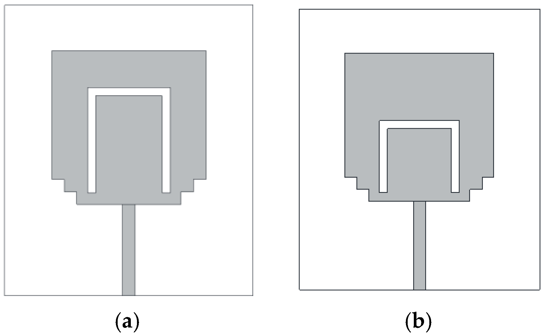
According to the discussion above, it is reasonable to combine these sensor units with different lengths of U-slot and different lengths of meander microstrip line for increasing sensing signature designated to enhance information capacity by joint spectral and temporal modulation. For a real embodiment of such a sensor, it is possible to embed a sensor head with one across the U-slot and another connected at the end of the meander microstrip line. This sensor head can function as the ON/OFF switch that determines the availability of the band gap frequency and the status phase of the reflected pulse (0° or 180°), which enables one combined sensor unit to have digits by two bits. If these four different sensor units are configured in a cubic way, the sensor can have a digital capacity total of up to eight bits. The designed sensor units used to combine the sensor are shown in
Figure 13, where
Figure 13a represents that the U-slot length is 12.7 mm combined with the microstrip line length of 11 mm;
Figure 13b represents that the U-slot length is 9 mm combined with the microstrip line length of 31 mm;
Figure 13c represents that the U-slot length is 6.5 mm combined with the microstrip line length of 41 mm;
Figure 13d represents that the U-slot length is 5.15 mm combined with the microstrip line length of 51 mm.
6. Sensor Fabrication and Performance Verification
The sensor units illustrated in
Figure 13 are combined and fabricated, as shown in
Figure 14. The performance of the sensor is verified by measurement in the chamber, as shown in
Figure 15. The results of the performance of the band gap frequency for modulation and coding in the spectral domain and the results of the performance of the reflected pulses for modulation and coding in the time domain are shown in
Figure 16 and
Figure 17. The simulation and measurement are in agreement, indicating after the decision that the U-slots in a and c units are equal to the opening state, which forms band gap frequencies with respect to 7.07 GHz and 4.95 GHz, coded in the spectral domain by 1. However, the ends of the meander microstrip lines in a and c units are equal to the opening state, which has a phase gap toward the interrogating pulse by 0 degrees, coded in the temporal domain by 0. The U-slot in b and d units are also equal to the opening state, which forms band gap frequencies with respect to 6.07 GHz and 3.96 GHz, coded in the spectral domain by 1. However, the ends of the meander microstrip lines in b and d units are equal to the shorting state, which has a phase gap toward the interrogating pulse by 180 degrees, coded in the temporal domain by 0. The code that the sensor has can be enhanced by eight bits in the sequence of spectral–temporal joint coding, denoting 10-11-10-11.
The comparison of the proposed sensor with various passive wireless sensors is shown in
Table 1.
7. Conclusions
The UWB signal can render plentiful signatures for UWB sensors with enhanced information capacity. For that, this paper designs and develops a passive wireless sensor through the combination of multiple sensor units operated in the principle of spectral–temporal joint coding and modulation. A prototype of the proposed sensor is configured by four UWB sensor units, each of them is specified by joint modulation upon the UWB pulse in the time domain and, simultaneously, the UWB spectrum in the frequency domain, coded by 1/0 data, delivering a total enhanced capacity of up to eight bits. Simulation and measurement verify the validation of the UWB sensor and the effectiveness of digital data delivery. The application of this UWB sensor is tailored for scenarios with rigorous environments, dangerous working plants, and sites where power cannot be accessed easily. Therefore, this sort of remote, contactless, and battery-free sensor proposed in this study is quite necessary for this sensing application, which is required for long-term availability and sustainability.
Author Contributions
Conceptualization, R.L.; Validation, J.L.; Investigation, R.L.; Resources, R.L.; Writing—original draft, R.L.; Supervision, X.H.; Project administration, X.H. All authors have read and agreed to the published version of the manuscript.
Funding
This research was funded by The National Natural Science Foundation of China, grant number 62271386.
Data Availability Statement
The original contributions presented in this study are included in the article. Further inquiries can be directed at the corresponding author.
Conflicts of Interest
The authors declare no conflict of interest.
References
- He, D.; Cui, Y.; Ming, F.; Wu, W. Advancements in passive wireless sensors, materials, devices, and applications. Sensors 2023, 23, 8200. [Google Scholar] [CrossRef] [PubMed]
- Kumar, H. Wireless sensor networks in healthcare system: A systematic review. Wirel. Pers. Commun. 2024, 134, 1013–1034. [Google Scholar] [CrossRef]
- Floris, I.; Adam, J.M.; Calderón, P.A.; Sales, S. Fiber optic shape sensors: A comprehensive review. Opt. Lasers Eng. 2021, 139, 106508. [Google Scholar] [CrossRef]
- Nelson, B.D.; Karipott, S.S.; Wang, Y.; Ong, K.G. Wireless technologies for implantable devices. Sensors 2020, 20, 4604. [Google Scholar] [CrossRef] [PubMed]
- Mulloni, V.; Donelli, M. Chipless rfid sensors for the internet of things: Challenges and opportunities. Sensors 2020, 20, 2135. [Google Scholar] [CrossRef] [PubMed]
- Raju, R.; Bridges, G.E.; Bhadra, S. Wireless passive sensors for food quality monitoring: Improving the safety of food products. IEEE Antennas Propag. Mag. 2020, 62, 76–89. [Google Scholar] [CrossRef]
- Girbau, D.; Ramos, A.; Lazaro, A.; Rima, S.; Villarino, R. Passive wireless temperature sensor based on time-coded uwb chipless rfid tags. IEEE Trans. Microw. Theory Tech. 2012, 60, 3623–3632. [Google Scholar] [CrossRef]
- Verma, G.; Mondal, K.; Gupta, A. Si-based MEMS resonant sensor: A review from microfabrication perspective. Microelectron. J. 2021, 118, 105210. [Google Scholar] [CrossRef]
- Boyer, C.; Roy, S. —Invited paper—Backscatter communication and RFID: Coding, energy, and MIMO analysis. IEEE Trans. Commun. 2014, 62, 770–785. [Google Scholar] [CrossRef]
- Khan, S.R.; Bernassau, A.L.; Desmulliez, M.P.Y. Passive and battery-free RFID-based wireless healthcare and medical devices: A review. IEEE J. Radio Freq. Identif. 2024, 8, 724–742. [Google Scholar] [CrossRef]
- Saeidi, T.; Ismail, I.; Wen, W.P.; Alhawari, A.R.H.; Mohammadi, A. Ultra-wideband antennas for wireless communication applications. Int. J. Antennas Propag. 2019, 2019, 7918765. [Google Scholar] [CrossRef]
- Kumar, G.; Kumar, R. A survey on planar ultra-wideband antennas with band notch characteristics: Principle, design, and applications. AEU Int. J. Electron. Commun. 2019, 109, 76–98. [Google Scholar] [CrossRef]
- Mekki, K.; Necibi, O.; Dinis, H.; Mendes, P.; Gharsallah, A. Investigation on the chipless RFID tag with a UWB pulse using a UWB IR-based reader. Int. J. Microw. Wirel. Technol. 2021, 14, 1–10. [Google Scholar] [CrossRef]
- Liu, G.; Wang, Q.A.; Jiao, G.; Dang, P.; Nie, G.; Liu, Z.; Sun, J. Review of wireless RFID strain sensing technology in structural health monitoring. Sensors 2023, 23, 6925. [Google Scholar] [CrossRef] [PubMed]
- Mc Gee, K.; Anandarajah, P.; Collins, D. A review of chipless remote sensing solutions based on RFID technology. Sensors 2019, 19, 4829. [Google Scholar] [CrossRef] [PubMed]
- Subrahmannian, A.; Behera, S.K. Chipless RFID: A unique technology for mankind. IEEE J. Radio Freq. Identif. 2022, 6, 151–163. [Google Scholar] [CrossRef]
- Yadav, M.V.; Baudha, S. A miniaturized printed antenna with extended circular patch and partial ground plane for UWB applications. Wirel. Pers. Commun. 2021, 116, 311–323. [Google Scholar] [CrossRef]
- Dehmas, M.; Azrar, A.; Challal, M.; Djafri, K.; Mouhouche, F.; Settou, N.; Zouari Ferhat, H. A Novel UWB Printed Monopole Antenna with Enhanced Frequency Bandwidth. In Proceedings of the 2022 2nd International Conference on Advanced Electrical Engineering (ICAEE), Constantine, Algeria, 29–31 October 2022. [Google Scholar]
- Arpitha, M.M.; Sethy, P.; Behera, S.K. A 5-Bit Rectangular Resonator Array for Biomedical Applications. In Proceedings of the 2022 3rd International Conference for Emerging Technology, INCET 2022, Belgaum, India, 15 July 2022. [Google Scholar]
- Mishra, D.P.; Kumar Das, T.; Sethy, P.; Behera, S.K. Design of a multi-bit chipless RFID tag using square split-ring resonators. In Proceedings of the 2019 IEEE Indian Conference on Antennas and Propagation, InCAP 2019, Ahmedabad, India, 19–22 December 2019. [Google Scholar]
- Habib, A.; Afzal, M.A.; Sadia, H.; Amin, Y.; Tenhunen, H. Chipless RFID tag for IoT applications. In Proceedings of the 2016 IEEE 59th International Midwest Symposium on Circuits and Systems (MWSCAS), Abu Dhabi, United Arab Emirates, 16–19 October 2016. [Google Scholar]
- Adbulkawi, W.M.; Sheta, A.-F.A. Printable Chipless RFID Tags for IoT Applications. In Proceedings of the 1st International Conference on Computer Applications and Information Security, ICCAIS 2018, Riyadh, Saudi Arabia, 4–6 April 2018. [Google Scholar]
Figure 1.
Illustration of the Sensor Unit. (a) Top view. (b) Bottom view. (Unit: mm).
Figure 1.
Illustration of the Sensor Unit. (a) Top view. (b) Bottom view. (Unit: mm).
Figure 2.
Sensor Unit’s S11 parameter.
Figure 2.
Sensor Unit’s S11 parameter.
Figure 3.
Sensor Unit with U-slot (a) without sensor head (b) with sensor head.
Figure 3.
Sensor Unit with U-slot (a) without sensor head (b) with sensor head.
Figure 4.
Sensor Unit’s S11 parameter with and without U-slot.
Figure 4.
Sensor Unit’s S11 parameter with and without U-slot.
Figure 5.
Sensor Unit’s S11 parameter when U-slot is shortened.
Figure 5.
Sensor Unit’s S11 parameter when U-slot is shortened.
Figure 6.
Sensor Unit with meander line (a) open end with sensor head (b) short end with sensor head.
Figure 6.
Sensor Unit with meander line (a) open end with sensor head (b) short end with sensor head.
Figure 7.
Pulses at the time domain.
Figure 7.
Pulses at the time domain.
Figure 8.
Pulses at the time domain. (a) Impedance match ends. (b) Impedance mismatch ends by short.
Figure 8.
Pulses at the time domain. (a) Impedance match ends. (b) Impedance mismatch ends by short.
Figure 9.
Structures of the four frequency domain modulations (a) The length of U-slot 12.7 mm (b) The length of U-slot 9 mm (c) The length of U-slot 6.5 mm (d) The length of U-slot 5.15 mm.
Figure 9.
Structures of the four frequency domain modulations (a) The length of U-slot 12.7 mm (b) The length of U-slot 9 mm (c) The length of U-slot 6.5 mm (d) The length of U-slot 5.15 mm.
Figure 10.
Comparison of band gap’s characteristics at the four assigned frequencies(U-slot).
Figure 10.
Comparison of band gap’s characteristics at the four assigned frequencies(U-slot).
Figure 11.
Sensor units of the four time domain modulations. (a) The length of the microstrip line is 11 mm. (b) The length of the microstrip line is 31 mm. (c) The length of the microstrip line is 41 mm. (d) The length of the microstrip line is 51 mm.
Figure 11.
Sensor units of the four time domain modulations. (a) The length of the microstrip line is 11 mm. (b) The length of the microstrip line is 31 mm. (c) The length of the microstrip line is 41 mm. (d) The length of the microstrip line is 51 mm.
Figure 12.
Comparison of the reflected pulse received by four different lengths of the microstrip line.
Figure 12.
Comparison of the reflected pulse received by four different lengths of the microstrip line.
Figure 13.
Schematics of the sensor unit with enhanced multi-bits based on UWB’s Spectral–Temporal Joint Coding and Modulation. (a) U-slot (12.7 mm) combined with the microstrip line (11 mm). (b) U-slot (9 mm) combined with the microstrip line (31 mm). (c) U-slot (6.5 mm) combined with the microstrip line (41 mm). (d) U-slot (l5.15 mm) combined with the microstrip line (51 mm).
Figure 14.
The Fabrication of sensor (a) front side, (b) back side.
Figure 14.
The Fabrication of sensor (a) front side, (b) back side.
Figure 15.
Sensor measurement and performance verification (a) front side, (b) back side.
Figure 15.
Sensor measurement and performance verification (a) front side, (b) back side.
Figure 16.
The performance of band gap frequency for modulation and coding in the spectral domain.
Figure 16.
The performance of band gap frequency for modulation and coding in the spectral domain.
Figure 17.
The performance of the reflected pulses for modulation and coding in the time domain.
Figure 17.
The performance of the reflected pulses for modulation and coding in the time domain.
Table 1.
The Comparison of the Proposed Design with Other Multi-Bit Sensors.
Table 1.
The Comparison of the Proposed Design with Other Multi-Bit Sensors.
| | Frequency Band (GHz) | Bit Capacity (bit) | Modulation Type | Architecture Type | Application |
|---|
| [19] | 1.9/2.4/3.7/5.4/9.5 | 5 | Spectral domain | Planar array | ISM/Biomedical |
| [20] | 0.8~0.9/3.1~10.6 | 3 | Spectral domain | Planar | Retail/Biomedical/Industrial |
| [21] | 1.2~2.91 | 12 | Spectral domain | Planar | IoT |
| [22] | 6.1~6.6 | 6 | Spectral domain | Planar | IoT |
| Proposed sensor | 3.1~10.6 | 8 | Spectral domain/Temporal domain | 3D array | ISM/Industrial |
| Disclaimer/Publisher’s Note: The statements, opinions and data contained in all publications are solely those of the individual author(s) and contributor(s) and not of MDPI and/or the editor(s). MDPI and/or the editor(s) disclaim responsibility for any injury to people or property resulting from any ideas, methods, instructions or products referred to in the content. |
© 2025 by the authors. Licensee MDPI, Basel, Switzerland. This article is an open access article distributed under the terms and conditions of the Creative Commons Attribution (CC BY) license (https://creativecommons.org/licenses/by/4.0/).


