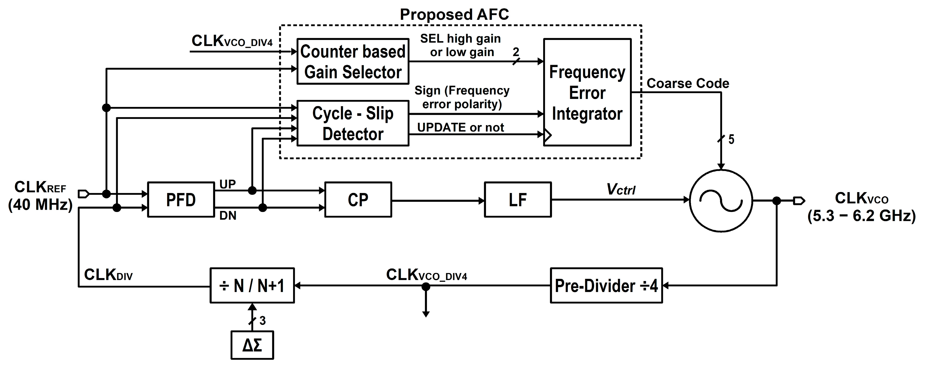
1. Introduction
As the performance of data communication systems continues to improve, the demand for low phase noise and fast clock generation has become increasingly important. A frequency synthesizer is widely used to generate precise clock frequency by synchronizing an on-chip voltage-controlled oscillator (VCO) to a stable reference. To maintain low phase noise and spur levels, recent synthesizers are designed with reduced VCO gain (
KVCO), which improves noise performance but narrows down the frequency tuning range. To compensate for the limited range, designers typically increase the number of coarse-tuning bits (code) by employing a coarse capacitor bank [
1]. As a result, the VCO’s total tuning range can be extended while maintaining low
KVCO. However, as the number of coarse-tuning codes increases, often reaching about 2
5–2
7 discrete coarse-tuning codes [
2,
3,
4], the calibration time required to locate the correct code also increases, making a fast and efficient automatic frequency calibration (AFC) indispensable. The AFC schemes digitally search the coarse-tuning code that contains the target frequency (
ftarget) before phase locking.
Along with the industry trend toward multi-band transceiver implementation with wide tuning range [
5], VCO frequency (
fVCO) drift, due to operating environment changes such as voltage and temperature (VT) variation, has become an issue [
6]. In the event of frequency drift where the initially selected coarse code no longer covers the target frequency, the loop should quickly find a new valid code within several adjacent coarse-tuning codes by using calibration algorithms. The designed cycle slip-based closed-loop AFC detects frequency offset in real time while keeping the loop active. In addition, it employs a variable gain calibration algorithm that increases the correction gain for large frequency offset conditions to increase convergence speed and decrease the gain near locking frequency for stable settling of the coarse code, achieving a convergence speed comparable to previous AFC techniques and enabling smooth, continuous lock operation even under frequency drift conditions. Operating in the 5.3–6.2 GHz frequency band, the synthesizer is well suited for Wi-Fi 6/6E and 5 GHz ISM-band wireless transceivers, which often require fast and reliable frequency switching during channel hopping. It is also suitable for high-performance clock-generation circuits used in SoC, industrial, and automotive environments, where temperature drift and mechanical vibration can influence frequency stability.
The paper is organized as follows.
Section 2 presents the designed AFC algorithm that corrects the synthesizer coarse code efficiently and discusses the motivation behind the implemented calibration scheme.
Section 3 explains its operation principle, and
Section 4 shows the implemented circuits of the synthesizer with the AFC.
Section 5 includes the measurement results, and conclusions are drawn in
Section 6.
3. Operation Principle of Designed AFC Algorithm
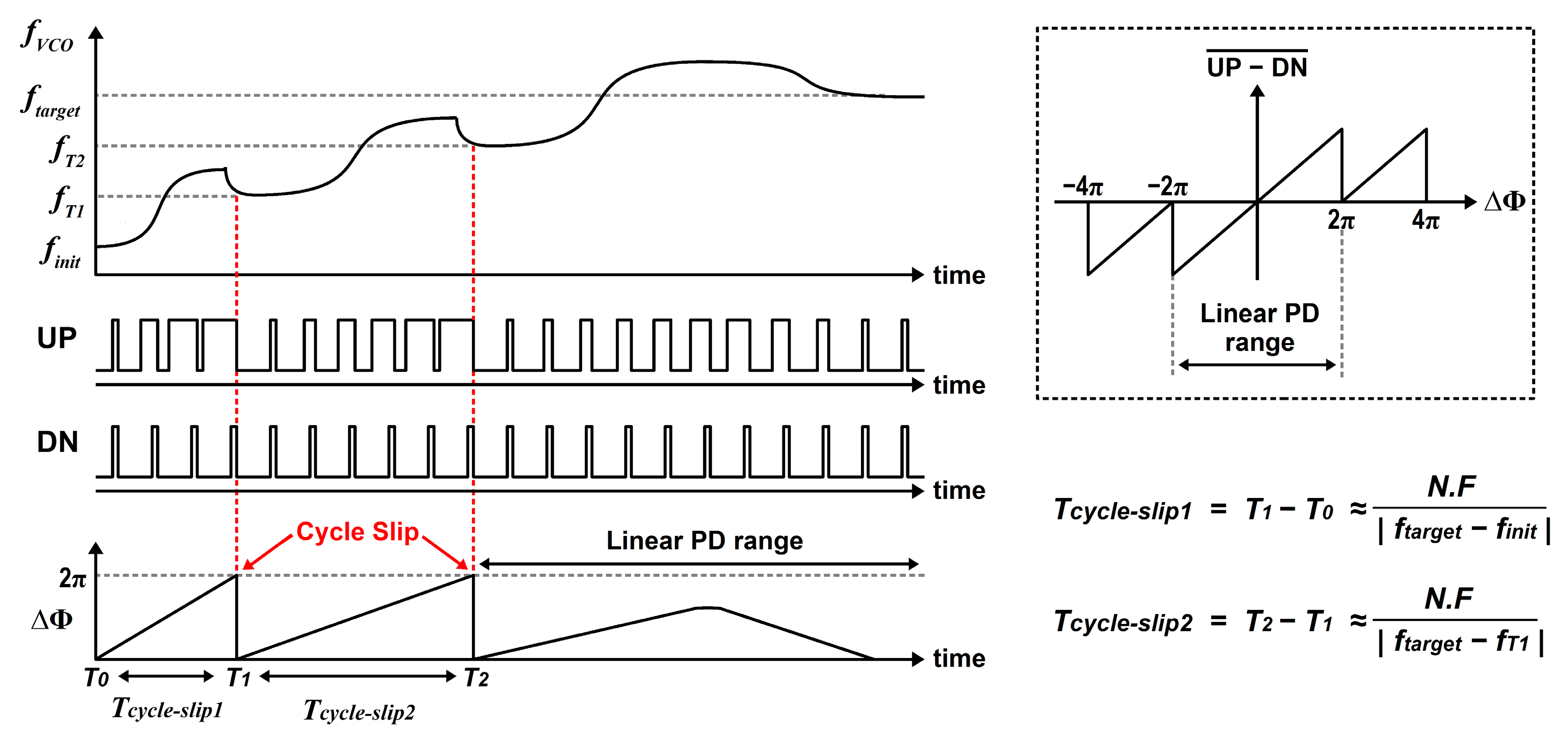
Figure 4 illustrates the
UP/DN waveforms of PFD for the cases that the initial VCO frequency (
finit) is far from the
ftarget during PLL lock. If the frequencies of the two PFD input clocks are far apart, either
UP or
DN pulse’s duty accumulates rapidly and another round of accumulation cycle restarts because the detection range of PFD is limited to 2π in a phase domain. The accumulation period can be expressed roughly as N.F/|
ftarget −
fTn | where N.F is a division ratio and
fTn is the VCO frequency at the start of a new accumulation cycle. The period gradually becomes longer as the
fTn approaches
ftarget, and finally the PLL enters into the linear PD range in which the PFD operates as a phase detector only and its operation range does not surpass beyond the 2π limit. Based on the occurrence of such cycle slips, the frequency information can be extracted within the closed loop. The AFC detects every “cycle slip” logically before the loop falls into the linear PD range and uses it as indicators of frequency error existence and the polarity of two input clock’s frequency offset.
Figure 5a shows the designed cycle slip detector that monitors if there is a frequency error between
CLKREF and
CLKDIV. The
UPDATE pulse is generated at the cycle slip timing by NANDing
UPA ⊕
UPB and
DNA ⊕
DNB, and it is used to trigger the entire AFC state machine. If the frequency locks, the
UPDATE pulse is no longer produced with the AFC turned off, and power can be saved afterward. However, the “frequency error detection logic” keeps monitoring the frequency offset with low power and is ready to restart the AFC to correct the coarse code of VCO whenever the frequency drift occurs.
Figure 5b presents the timing diagram of each node in the detection logic for a case of
fREF >
fDIV. The sign is produced by sampling the
DN signal by the
UP signal. The sign becomes 0 if
CLKREF leads
CLKDIV, and vice versa.
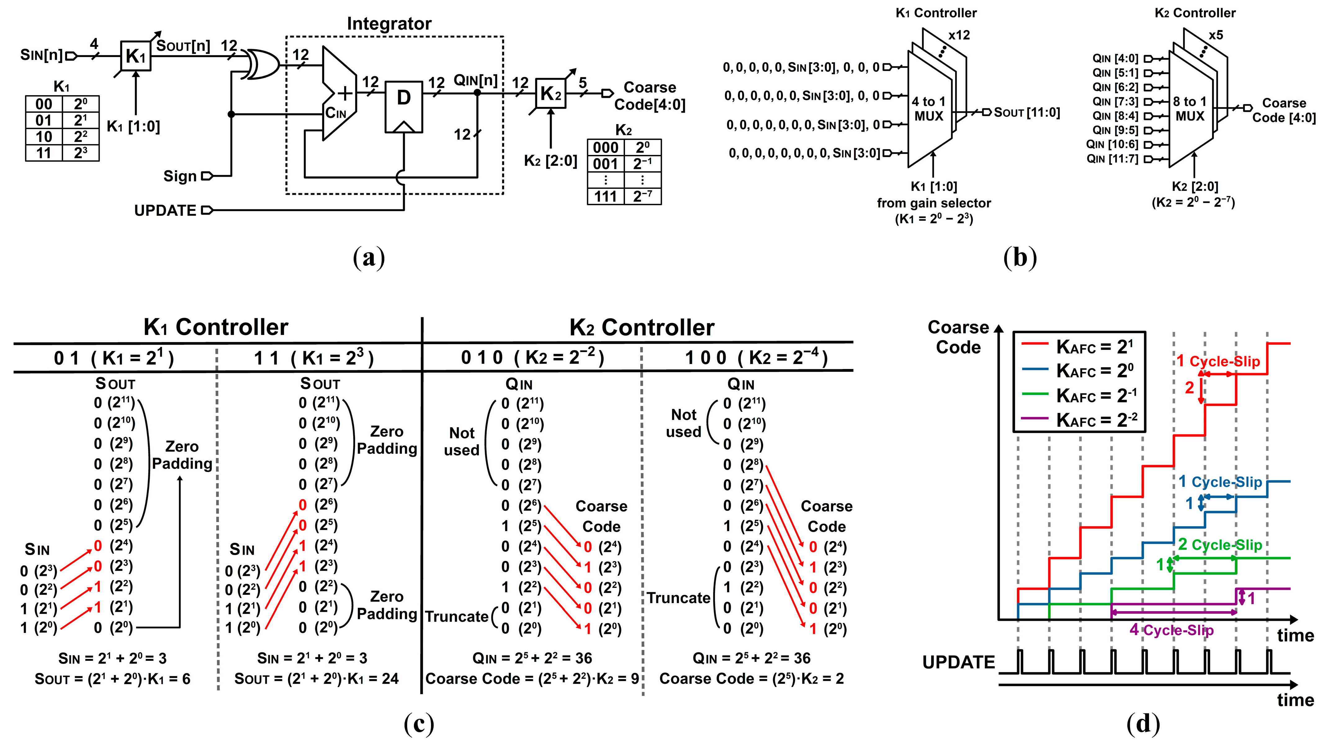
Figure 6a presents a circuit diagram of frequency error integrator in the designed AFC with a wide range of calibration gain control. The sign and input integrator gain
K1 (2
0–2
3) determines the polarity and magnitude of frequency error, and it is integrated afterward. Output integrator gain
K2 provides another degree of freedom to adjust the calibration gain with a range of 2
0–2
−7. Both
K1 and
K2 are implemented with binary-shifting multiplexers (MUXs), as shown in
Figure 6b.
Figure 6c illustrates the MUX connection mapping rules of
K1 and
K2 for gain control.
K1 controls the gain based on binary shift in S
IN [3:0], and the remaining bits of the output are padded with 0. In the event of toggling Q
IN LSB at the vicinity of frequency lock, which is undesirable for stable code convergence, lowering
K2 by truncation can prevent the toggling Q
IN LSB from being reflected on the coarse code directly. The total AFC gain (
KAFC) with
K1 and
K2 is defined as
Figure 6d illustrates behavior of the frequency error integration for
KAFC = 2
1, 2
0, 2
−1, and 2
−2 if the input S
IN value is set as +1. The whole AFC block is triggered by the
UPDATE pulse generated from the preceding PFD only when the cycle slip occurs. Once the PLL enters into the linear PD range, the whole AFC stops operating and the coarse code is fixed for a condition of
fREF ≈
fDIV with a high stability.
A low AFC gain (
KAFC,Low) would achieve a good calibration stability but degrade the calibration speed. In contrast, a high AFC gain (
KAFC,High) expedites the convergence speed while the stability is traded off, especially on the verge of completing the calibration. The variable gain calibration algorithm has two pre-defined gains, and the high or low gain mode is chosen depending on amount of frequency offset between
fVCO and
ftarget. As shown in
Figure 7a, the gain selector continuously monitors the frequency offset (
ΔN) using a counter. It then compares
ΔN with a pre-set threshold (
Nth) to choose the gain mode. The variable gain control ensures stable calibration for small frequency offsets while reducing the calibration time for large frequency offsets.
Figure 7b illustrates an AFC operation with the variable gain transition. Initially, the adaptation begins with a calibration speed of
KAFC,High for fast convergence. As the VCO approaches the target frequency, the gain is switched to
KAFC,Low within the threshold frequency (
fth) offset to accomplish a good stability while trading off the calibration speed. Even in the event of frequency drift, the lock recovers within several adjacent coarse code values with
KAFC,Low smoothly. If the
fth is too wide, calibration time increases because the AFC would operate with
KAFC,Low for a longer time. If it is too narrow, the coarse code update may become unstable, and it can lead to the failure of frequency lock.
The designed AFC shown in
Figure 8 performs both digital coarse calibration (digital coarse path) and analog fine calibration (analog
Vctrl path) concurrently in the closed loops; so, the convergence speeds of the two paths should be carefully designed. Unless the convergence speeds of the two paths are appropriately managed, the PLL may end up with an unstable or a low-speed calibration. Therefore, it is necessary to analyze the variation rate of
Vctrl determined by the loop dynamics.
Figure 9 illustrates the increase in
Vctrl with respect to the various frequency offset conditions or constant phase offset
ΔΦ = π at the PFD input, where
Vctrl (t) =
ΔΦ · I
CP · t/(2π · C
P) [
9]. With a frequency offset,
ΔΦ gradually increases from 0 to 2π over one cycle slip period and its average phase offset can be regarded as π (
ΔΦ = π,
Δf = 0 case) in the long time regardless of various frequency offset values (
Δf = 0.2, 0.4, 0.8 MHz case). The full-scale transition time of the analog
Vctrl path is roughly 4.8 μs (≈ 2π · 200 pF · 1.2 V/(π · 100 μA)) in our IP.
The single coarse code transition time of the cycle slip-based digital coarse path is given by 1/(
KAFC ×
Δf). The coarse code step size (
KAFC) per cycle slip can be digitally controlled and it allows the transition time of the digital coarse path to be independently tuned. The graph of
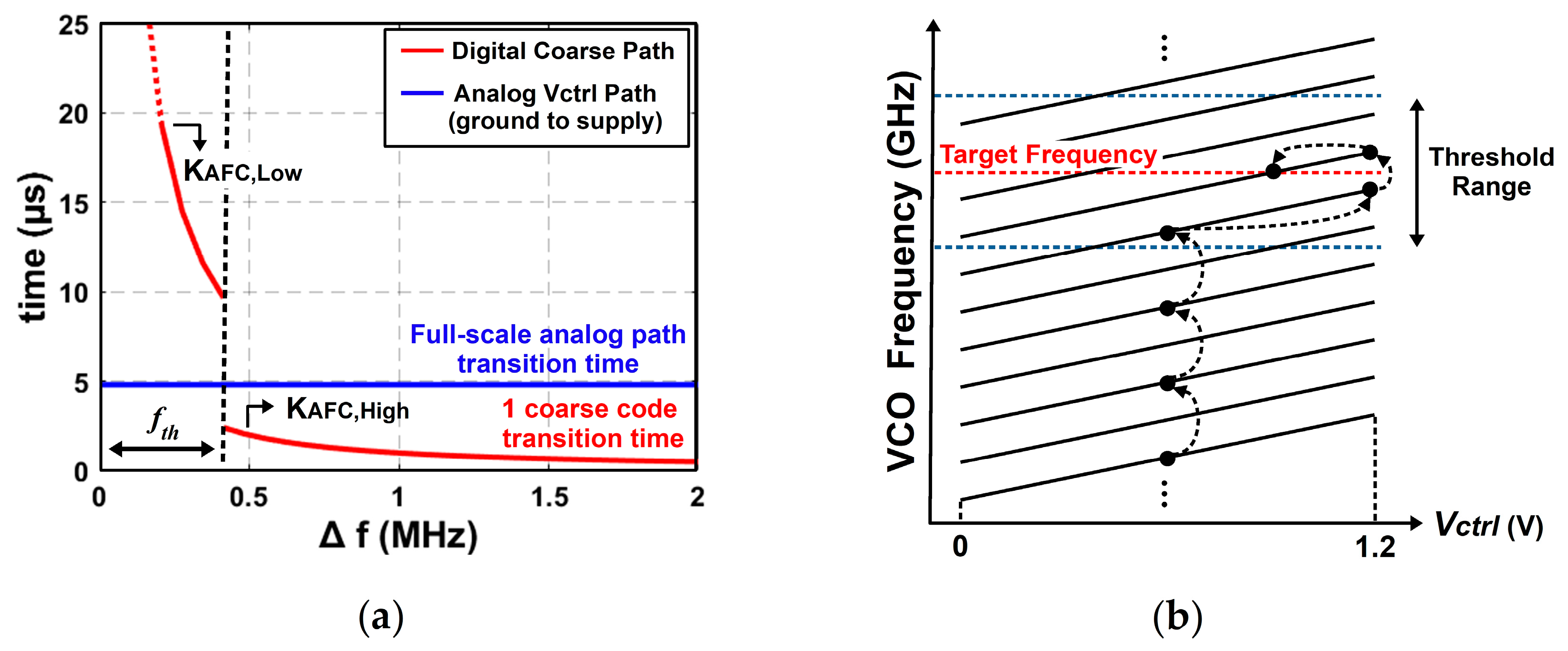
Figure 10a compares the frequency transition time of the analog
Vctrl from GND to VDD and one coarse code transition time at various frequency offset positions. If the frequency offset is larger than
fth, the frequency transition speed of the digital coarse path is faster than the analog
Vctrl path. On the other hand, inside the threshold
fth range, the AFC gain is intentionally reduced so that the analog
Vctrl path moves quickly, which makes the analog path complete the convergence stably.
Figure 10b illustrates the AFC operation on the VCO profile, considering the speeds of two paths. Outside the threshold range, the coarse code transitions rapidly, while the analog
Vctrl almost remains at a certain voltage due to its lower speed. However, inside the threshold, the
Vctrl moves faster and reaches either VDD or VSS before the coarse code changes. After the coarse code converges, the PLL operates in the loop dynamics and begins linear phase lock without coarse code transitions.
Vctrl moves from VDD or VSS to the target analog voltage. Through the convergence speed management, the AFC achieves a stable lock without code toggling and reduced overall calibration time.
The calibration time in the variable gain calibration algorithm is more accurately calculated as the cumulative sum of each cycle slip period, and it consists of
TAFC,step1 and
TAFC,step2. With each coarse code change, the frequency offset decreases by
KAFC,High ×
fspacing in step 1 (high gain mode) and
KAFC,Low ×
fspacing in step 2 (low gain mode) as
fVCO approaches
ftarget. Assuming a constant
fspacing, the convergence time in each step can be expressed as
where
Dcodi is the decimal value of the code distance between the target coarse code and the initial starting coarse code, and A and B are the quotient and the remainder of
Dcodi/
KAFC,High, respectively. The AFC updates the coarse VCO code with “A” sequential rounds in step 1 and with “B” sequential rounds in step 2. The total calibration time is given by
TAFC =
TAFC,step1 +
TAFC,step2.
The calibration time depends on the
Dcodi. To compute the calibration time generally, the average calibration time over all
Dcodi values is defined as
where
n is the number of bits in the coarse VCO code, and
TAFC,avg =
TAFC,step1,avg +
TAFC,step2,avg.
TAFC,step1,avg and
TAFC,step2,avg denote the arithmetic means over
KAFC,High ≤
Dcodi < 2
n (outside threshold) and 0 ≤
Dcodi <
KAFC,High (inside threshold), respectively.
Figure 11 shows the calculated
TAFC,avg under various
KAFC settings. If
KAFC,High =
KAFC,Low = 2
0, it indicates that the AFC operates without gain selector (1-step calibration). Notice that using the gain selector by setting
KAFC,High = 2
1 and
KAFC,Low = 2
0 reduces the average calibration time by approximately half when it is used. If
KAFC,High is set too high, the threshold range should be set as a high value for stability as well, which can increase the time spent in step 2. By properly setting
KAFC,Low,
KAFC,Low, and
Nth (
fth), the calibration can be completed within an average of 5–6 μs in our IP parameters. Unlike the designed AFC, conventional AFC using an open-loop binary search algorithm requires a total calibration time defined as
n × (
Tidle +
Tmeas), which results in approximately 8 μs for a 7-bit coarse VCO code [
10], where
Tidle is the intentionally inserted idle time allowing VCO clock to settle and
Tmeas is the frequency counting time. If scaled down to 5-bit, the calibration time becomes approximately 5.71 μs, which is comparable to the designed AFC set to
KAFC,High = 2
2,
KAFC,Low = 2
0.
Figure 12 shows the measured VCO output frequency and
fspacing at
Vctrl = 0.6 V. Unlike the constant
fspacing assumption, the measured
fspacing varies from 21 to 38 MHz and is non-uniform. Based on the measured data, a manual calculation that considers
fspacing variation under
KAFC,High = 2
2 and
KAFC,Low = 2
0 shows that
TAFC,avg increases from 6.45 μs to 6.82 μs (+5.8%). The increase mainly comes from smaller
fspacing in low coarse code region, and overall, the deviation is modest.
4. Circuit Design
Figure 13a shows the implemented LC-VCO structure that has a tuning range of 5.3–6.2 GHz. The VCO is designed to achieve a low
KVCO using a 5-bit coarse metal–insulator–metal (MIM) capacitor bank. The Widler feedback tail structure fixes the V
X node to a constant voltage level and the drain voltages of M
1 and M
2 are biased to VDD, and a variable poly resistor R
1 controls the tail current and, thus, output swing. M
1 and M
2 operate in either the cut-off or saturation region and it reduces the variation in parasitic capacitance, enabling low phase noise performance [
11,
12,
13].
Figure 13c presents the simulated tail current of the VCO under VT variation, showing that the current remains nearly constant due to the inherent temperature robustness of the Widlar tail current configuration. The structure effectively stabilizes the VCO bias point against thermal variation. To achieve high output swing and low flicker noise, an NMOS-only g
m-cell structure is used. But since the topology applies a VDD-level output bias, the linear range of the varactor is limited. Adding a ground bias in the varactor bank cancels nonlinearities from both branches in opposite directions and enhances the overall V-to-C linearity of the varactor bank [
12,
13,
14].
Figure 13b shows the measured VCO frequency characteristics with a tuning range of 5.3–6.2 GHz and a
KVCO of 65–100 MHz/V across the entire sub-band tuning curve.
Figure 14 presents a detailed circuit diagram of the implemented charge pump. A 3-bit binary-weighted switching structure controls MOSFET M
1–M
3 to generate variable output charge pump currents from 50 to 220 μA. To improve current mismatch and to increase output impedance, an opamp-based feedback structure is employed [
15]. Additionally, using dummy MOSFETs (M
4–M
10) preserves the symmetry of
UP/
DN branches for reduced mismatch and reference spur. The transconductance simulation results presented in
Figure 15 show that the charge pump operates linearly from approximately 0.1–1.1 V at an output current of 50 µA (CP gain code 000) and 0.2–1.0 V at 220 µA (CP gain code 111). The current mismatch percentage, calculated as 2 × |
IUP −
IDN|/(
IUP +
IDN) × 100 (%), remains within ±0.5% across the
Vctrl linear range. At
CPout = 0.6 V, the simulation results under VT variation show that, although a slight difference appears due to changes in the operating region with supply voltage variation, the charge pump maintains a wide linear range of approximately 1 V and low current mismatch percentage. The charge pump was optimized at room temperature and, a slight increase in current mismatch is observed under temperature variation due to the imbalance in the driving capability between the NMOS and PMOS switches. Because the charge pump maintains linear operation over a wide control voltage range, The operating
Vctrl point variation for various frequencies tuning has a limited impact on the noise performance variation, and similar noise levels are measured across various coarse code and
Vctrl operating conditions.
Figure 16 shows the die photograph of the frequency synthesizer with the implemented AFC. The chip is designed and fabricated in a 65 nm CMOS process, and all synthesizer components including the loop filter are implemented on-chip. The active area is 0.603 mm
2, in which the AFC occupies 0.018 mm
2.
5. Measurement Results
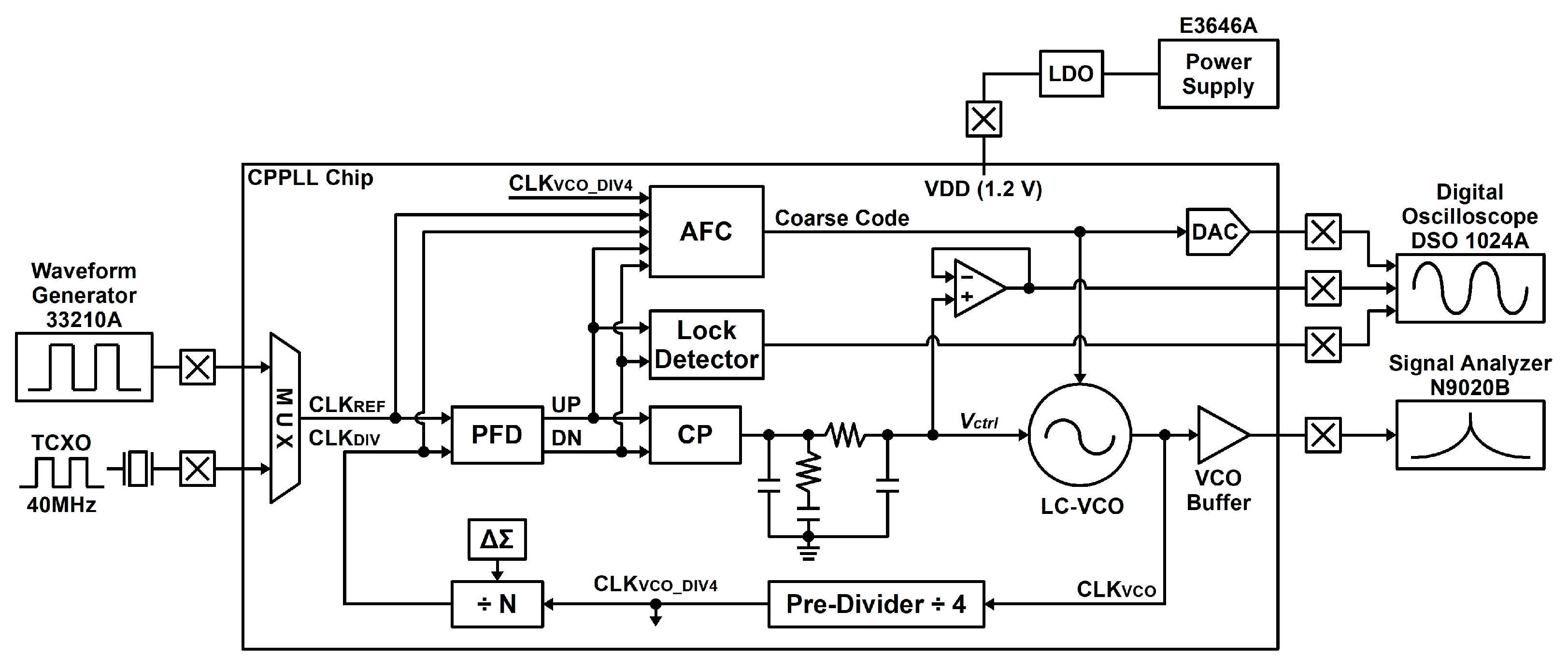
Figure 17 describes the measurement environment settings for the implemented frequency synthesizer. An E3646A power supply supplies 1.2 V VDD. The 40 MHz TCXO provides the reference clock, but a 33210A waveform generator is used when various reference frequencies are required. The digital-to-analog converter (DAC) converts the 5-bit coarse code into an analog voltage in real time. A 1024A digital oscilloscope monitors the coarse code (DAC output), the lock detector (LD) output, and the
Vctrl node to observe the PLL lock process and the AFC operation. An N9020B signal analyzer measures phase noise and spurs for the buffered VCO output (
CLKVCO).
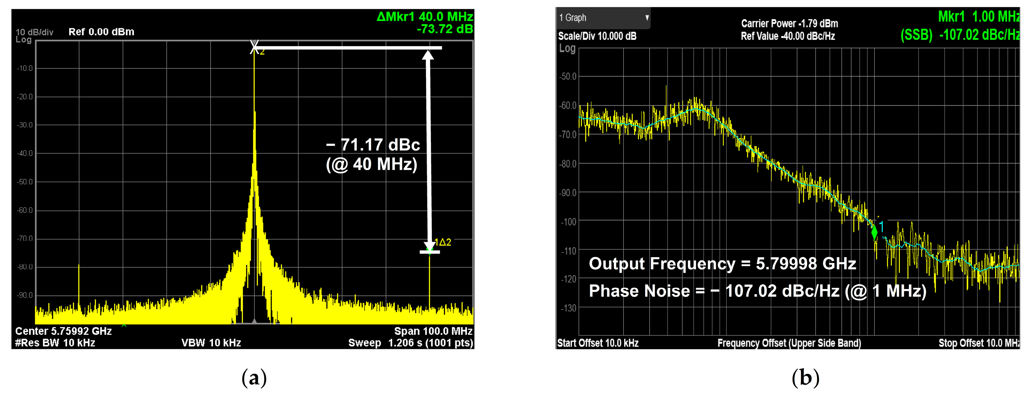
Figure 18a shows the measured reference spur of −71.17 dBc, resulting from improved current matching in the charge pump. The measured phase noise profile at a carrier frequency of 5.8 GHz is shown in
Figure 18b, which presents −107.02 dBc/Hz at 1 MHz offset. As shown in
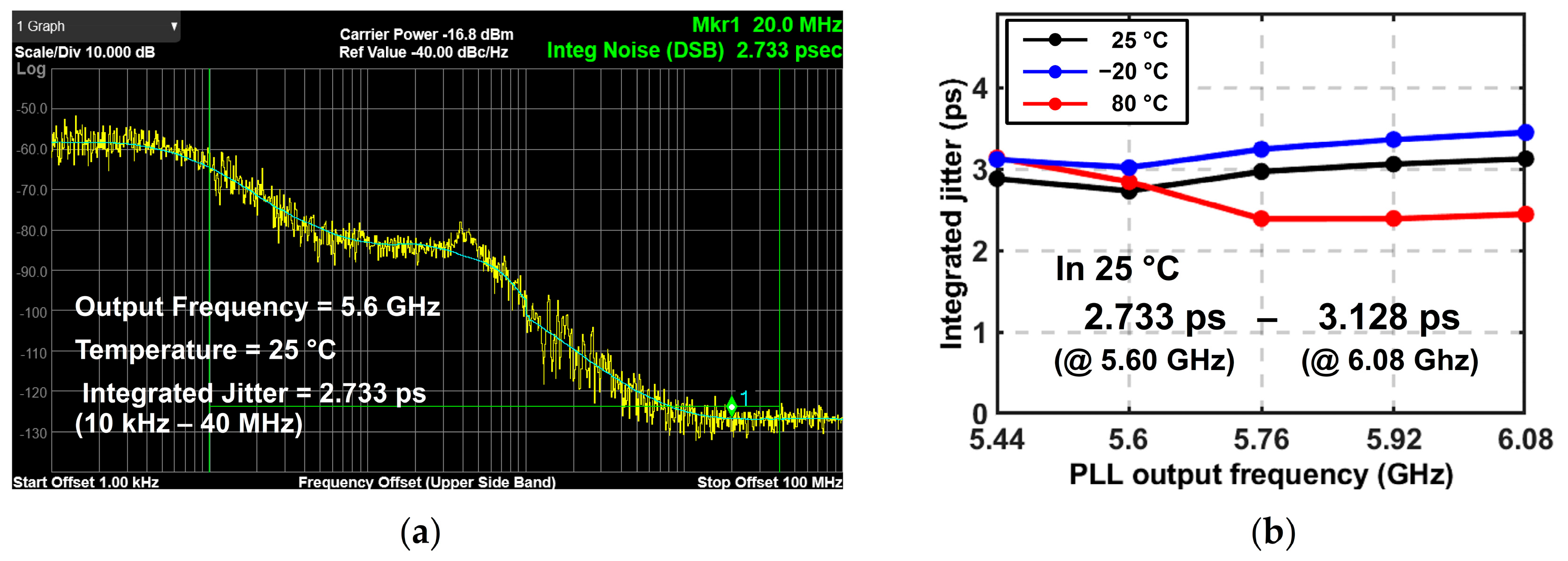
Figure 19a, the measured integrated jitter, over a 10 kHz–40 MHz offset range, is 2.733 ps at 5.60 GHz.
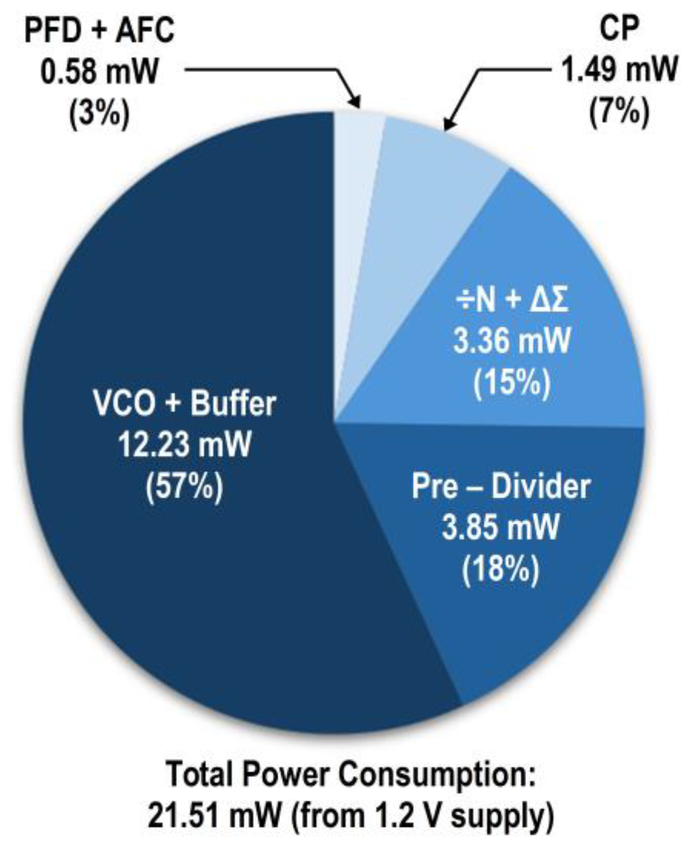
Figure 19b presents the integrated jitter results across the PLL output frequency range and under temperature variation, showing measured values of 2.733 ps at 5.60 GHz and 3.128 ps at 6.08 GHz in 25 °C. The overall jitter slightly increases at low temperature due to the temperature dependence of the loop dynamics, where the relative contributions of VCO noise and in-band noise vary with temperature, resulting in subtle changes in the effective loop bandwidth and noise-filtering characteristics. The synthesizer consumes 21.51 mW from a 1.2 V supply at the operation frequency of 5.8 GHz, and the power breakdown is shown in
Figure 20. Excluding the VCO output buffer, the power consumption is measured as 17.95 mW. The AFC consumes 0.54 mW, which can be powered down after the calibration. The total power varies within ± 5% over the output frequency range of 5.3 to 6.2 GHz.
Figure 21a shows the measured
Vctrl node voltage and the lock detector output during the AFC process, and the locations of
Vctrl and lock detector output nodes are described in
Figure 17. The coarse code calibration time is set by the AFC as it finds the appropriate coarse code. Outside the frequency threshold, the coarse code transitions faster than the
Vctrl. Inside the threshold,
Vctrl quickly moves and saturates near ground while the coarse code transitions. The measured frequency calibration time at target frequency 5.8 GHz with
KAFC,High = 2
2 and
KAFC,Low = 2
0 is 5.28 µs. Once the coarse code reaches the target code, the loop enters linear phase lock, and the linear
Vctrl lock time is mainly determined by the loop bandwidth as
Vctrl moves from ground to the target analog voltage. The total calibration lock time (coarse code calibration time + linear
Vctrl lock time) is 12.5 µs.
Figure 21b presents the average calibration time based on 30 measurements for each
KAFC setting. The results are comparable to the theoretical calculation in
Figure 11, and calibration is completed within an average of 5–6 μs for
KAFC,High = 2
2 and
KAFC,Low = 2
0.
Figure 21c shows the average calibration time measured across various output frequency bands using two separately implemented boards. The measured results show that the average calibration time remains consistently at 5–6 μs for both boards, regardless of the PLL output frequency. The consistency arises because, within the 5.3–6.2 GHz operating range, the sampling period of the internal counter in the gain selector remains constant, while the VCO frequency is divided by the ratio N.F (132–155) to generate the
UPDATE pulse that drives the AFC. As a result, the AFC operates at a nearly identical update rate across various frequencies, ensuring consistent calibration speed throughout various frequency bands.
Figure 21d presents the average calibration time measured under VT variation conditions at a target frequency of 5.8 GHz, with
KAFC,High = 2
2 and
KAFC,Low = 2
0. The measurement results demonstrate that the AFC maintains consistent calibration performance when both the supply voltage and temperature vary. This stable behavior is mainly attributed to the fully digital implementation of the AFC, which makes it inherently less sensitive to voltage and temperature fluctuations. The
UPDATE pulse that drives the calibration process is generated from the reference clock and divider output clock at relatively low frequencies, further contributing to the stability of the AFC operation across various frequency conditions.
Figure 22 presents the lock recovery behavior of the synthesizer during the frequency drift event. The test condition was emulated by rapidly changing the reference clock frequency, and the results demonstrate that as the output frequency deviates from the lock state, the AFC searches within several adjacent coarse-tuning codes to find a new coarse VCO code and successfully recovers the lock quickly and smoothly.
Table 2 compares the implemented frequency synthesizer performance and designed AFC technique with prior arts. The designed AFC maintains the closed-loop state during calibration, enabling comparable real-time tracking and correction of frequency drift as the other AFC scheme with closed-loop state. The AFC maintains closed-loop operation during calibration; the measured average calibration time of 5–6 µs is still modest, being comparable to that of open-loop AFC schemes. In the case of the open-loop AFC, when a frequency drift occurs, the loop must be disconnected and a full binary search repeated, leading to re-locking latency. In contrast, designed AFC corrects the deviation by updating only several adjacent coarse code values, enabling stable re-locking without frequency overshoot.

