1. Introduction
In recent years, the deployment of renewable energy sources has expanded rapidly worldwide, with solar photovoltaic (PV) systems undergoing significant growth. According to the International Energy Agency (IEA), the share of renewable energy in global electricity generation is likely to increase from 30% in 2023 to 46% in 2030 [
1]. The United States ranks among the top producers of solar electricity. There, small-scale PV systems account for approximately one-third of the total solar capacity, and nearly 70% of these installations are located in residential settings [
2]. However, many small-scale PV systems inject power into the grid regardless of the demand conditions. This results in local voltage fluctuations and an imbalance between supply and demand [
3]. To address such grid disturbances, Germany enacted the “Solar Peak Act” in February 2025. It imposes various operational constraints on PV systems. Similar policies are anticipated in other countries. As a countermeasure, Home Energy Management Systems (HEMSs) equipped with battery storage have gained attention as a means to stabilize residential power flow [
4,
5,
6,
7,
8,
9]. These systems can absorb surplus power and mitigate the reverse power flow by coordinating charge/discharge operations. Thereby, these support grid stability. For residential HEMSs applications, power conditioning systems (PCSs) are essential for bidirectional power conversion between batteries and the grid. In addition, owing to the installation space limitations, it is important to miniaturize the entire system [
10,
11]. These systems should be compact, efficient, and compliant with the grid interconnection standards. A critical requirement is fault ride-through (FRT). FRT is mandated in many countries to ensure grid stability during voltage disturbances [
12,
13]. Without FRT capabilities, the simultaneous disconnection or power reduction of distributed energy resources (DERs) during large-scale voltage dips or frequency deviations (such as those caused by transmission faults or generation outages) can result in subsequent failures throughout the power system. To prevent such instabilities, FRT requirements mandate that grid-connected systems maintain their operations during temporary disturbances. In Japan, the national Grid-interconnection Code mandates that DERs remain connected for at least 1.0 s following the onset of a voltage dip until the under-voltage relay (UVR) is permitted to activate [
14].
Figure 1 outlines the FRT timing requirements for the voltage dip. Although, systems may continue operation or cease energization during the fault, these should not disconnect before this duration. The post-fault response also varies depending on the retained voltage level.
Figure 2 illustrates the output power recovery requirements. For retained voltages of at least 20%, the system should recover at least 80% of the pre-fault output within 0.1 s after voltage restoration. For retained voltages below 20%, the output should recover to at least 80% of the pre-fault value within 0.2 s after voltage restoration. These requirements impose stringent constraints on PCS design, particularly under transient operating conditions.
To satisfy both physical constraints of residential installations and operational demands of FRT compliance, this paper proposes a compact and efficient PCS architecture that combines a three-level neutral point clamped (NPC) inverter with a dual active bridge (DAB) converter. In particular, the three-level NPC inverter plays a critical role in improving the system compactness. By lowering the voltage stress across each switching device, the NPC topology reduces the output voltage harmonics compared with conventional two-level inverters [
10,
15]. As a result, the required DC-link capacitor size can be reduced significantly, and the passive filter between the inverter and grid can be downsized. These advantages directly contribute to minimizing the installation footprint of a PCS. Therefore, the proposed system incorporates a three-level NPC inverter as the key component of its architecture. Considering the future expansion of HEMSs, galvanic isolation is essential to ensure both safety and functional compatibility with rooftop photovoltaic (PV) systems and electric vehicles (EVs), as emphasized in previous studies [
16,
17,
18]. To fulfill this requirement, the proposed system adopts DAB-based galvanic isolation. As shown in
Figure 3a, a conventional DAB converter consists of a single bridge that handles full-power transfer. This results in increased conduction losses at high loads. In contrast, the proposed system adopts an input-parallel output-series (IPOS) DAB configuration, as illustrated in
Figure 3b. This topology distributes the current among multiple input bridges. Thereby, it reduces the conduction losses and thermal stress [
19,
20]. The output series connection of the transformer improves the efficiency and insulation performance. Moreover, considering practical transformer characteristics such as leakage inductance and winding resistance, as well as the transient behavior of power devices, the IPOS topology is likely to provide further efficiency advantages.
In response to these challenges, this paper proposes a compact and grid-compliant PCS architecture for residential HEMSs applications. It incorporates a three-level NPC inverter and an IPOS-DAB converter. This architecture addresses the spatial and efficiency constraints of residential PCS design. Additionally, it facilitates broader renewable energy integration by ensuring compliance with stringent grid interconnection standards. The contributions of this study are as follows: First, a single-phase PCS architecture is proposed that combines a three-level NPC inverter and an IPOS-DAB converter. Unlike conventional PCS designs that employ the NPC topology solely for unidirectional operation, the proposed system enables bidirectional power transfer between the battery and grid. This allows both charging and discharging operations while maintaining stable grid interaction, which significantly extends the applicability of the NPC-based configuration. This configuration enhances both system compactness and conversion efficiency. Second, an adaptive output power control strategy is proposed to comply with the Japanese FRT regulations. Although several studies have investigated inverter control methods to satisfy FRT requirements, few have explicitly addressed how output power should be regulated during voltage dips [
21,
22,
23,
24,
25]. Thus, the proposed method maintains the discharging operation within the limits of the output current of the proposed PCS even under low-voltage conditions. This assists grid stability by supporting the local power supply during disturbances. Third, the proposed control strategy enables rapid power recovery after fault clearance. Thereby, it satisfies the FRT-defined recovery times with considerable margins. In particular, it ensures that the output power returns to at least 80% of the pre-fault level well before the deadlines stipulated for both moderate and severe voltage dips. To clarify the novelty of this study,
Table 1 summarizes a comparison between representative FRT-related control methods and the proposed PCS. Previous works have mainly focused on improving voltage stability or reactive current injection during voltage sags. However, few have discussed bidirectional power control or dynamic adjustment of output power to maintain the grid power balance. In contrast, the proposed system achieves both FRT compliance and power balancing with a simple control structure and compact design. Computer simulations were performed to evaluate the feasibility and effectiveness of the proposed control strategy. The simulation results reveal that the proposed PCS can maintain discharge operation during voltage dips while providing an appropriate output power within the current limit of the PCS and achieve rapid power restoration upon grid voltage recovery. These results indicate that the proposed system can enhance grid resilience and maintain power quality in residential low-voltage distribution networks.
3. Output Power Control Strategy of an IPOS DAB Converter to Satisfy FRT Requirements
An overview of the control method of the IPOS DAB converter is presented in
Section 2.2. However, a power control strategy is essential to satisfy the FRT requirements. This section explains the output power control method implemented in response to voltage dips in conjunction with the corresponding logic based on the retained voltage level. When a voltage dip occurs, maintaining a constant reference output power results in an increase in the inverter output current. The output power of the NPC inverter is the product of the output voltage
and current
, which can be expressed as
According to (
1), if the grid voltage decreases while keeping the power constant, the inverter current increases inversely with the voltage amplitude. For example, when the grid voltage drops to 50% of its nominal value, the current doubles to sustain the same output power. This increased current can exceed the rated current of the switching devices used in the inverter, which may trigger overcurrent protection or cause device failure. Therefore, appropriate power reduction during voltage dips is essential to satisfy the FRT requirements without violating the device limitations. The relationship between the instantaneous power on the DC and AC sides during a voltage dip can be expressed by the power balance equation as follows:
Here,
represents the DC-side power supplied from the DAB converter,
denotes the AC-side power injected into the grid, and
represents the power stored or released in the DC-link capacitor. Under normal operation,
holds, and the DC-link voltage remains nearly constant. However, during a voltage dip,
decreases and the balance is disturbed, causing
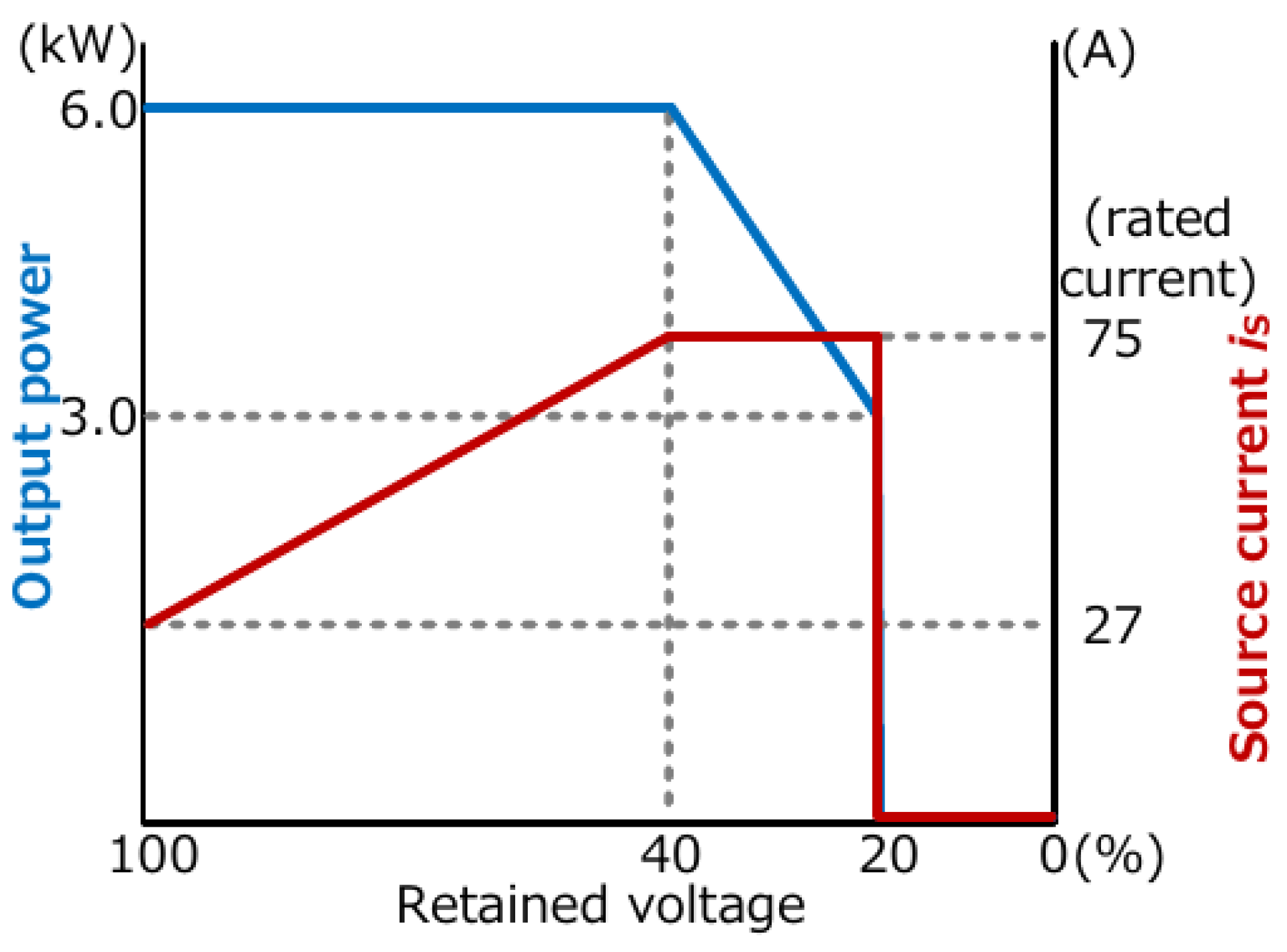
to fluctuate and the capacitor voltage to rise. One possible approach is to directly control the inverter output current; however, such a method requires coordination between the output current of inverter and the DC-link voltage regulation, resulting in a more complex control structure. Therefore, this study adopts a simplified configuration in which the system operation is achieved only by two control loops: the DC-link voltage control and the DC-side output power control of the DAB converter. This approach enables the proposed system to achieve FRT compliance while maximizing the inverter output power without exceeding the rated current of the switching devices even under voltage dip conditions. The rated current capacity of the switching devices used in the inverter should be considered when designing an output power control strategy that satisfies the FRT requirements without exceeding the device limitations. In this system, an Si-MOSFET (IXFK150N30P3) manufactured by IXYS is used as the switching device for the NPC inverter. Although the device has a continuous drain current rating of 150 A, practical operation typically requires a derating margin of approximately 70%. Accordingly, the upper limit of the inverter output current is set to 75 Arms. Based on this current limitation, the output power reference,
, is reduced adaptively according to the voltage retained during a voltage dip. This ensures that the inverter output current does not exceed a safe operating range. As illustrated in
Figure 7, when the retained voltage is above 40%, the corresponding current remains below the rated limit according to (
1). Therefore, the output power can be maintained at the rated 6.0 kW without risking overcurrent. In the range of 20–40%, however, maintaining constant power would require a current exceeding 75 Arms. Thus, the reference power
is reduced linearly so that the inverter output current remains within the safe operating limit. When the retained voltage decreases below 20%,
is set to zero to fully suspend the power flow. This prevents overcurrent risk and ensures FRT compliance.
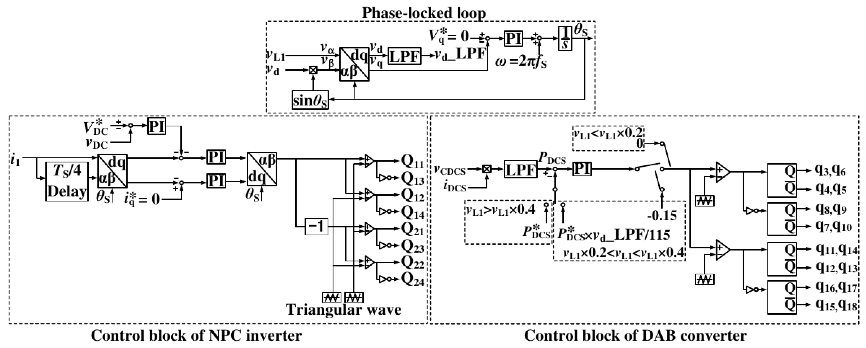
The output power control strategy described above is implemented using a control block in
Figure 5. This system detects the instantaneous voltage using
. It represents the instantaneous peak value of grid voltage
. Based on the magnitude of
,
is updated adaptively based on the magnitude of
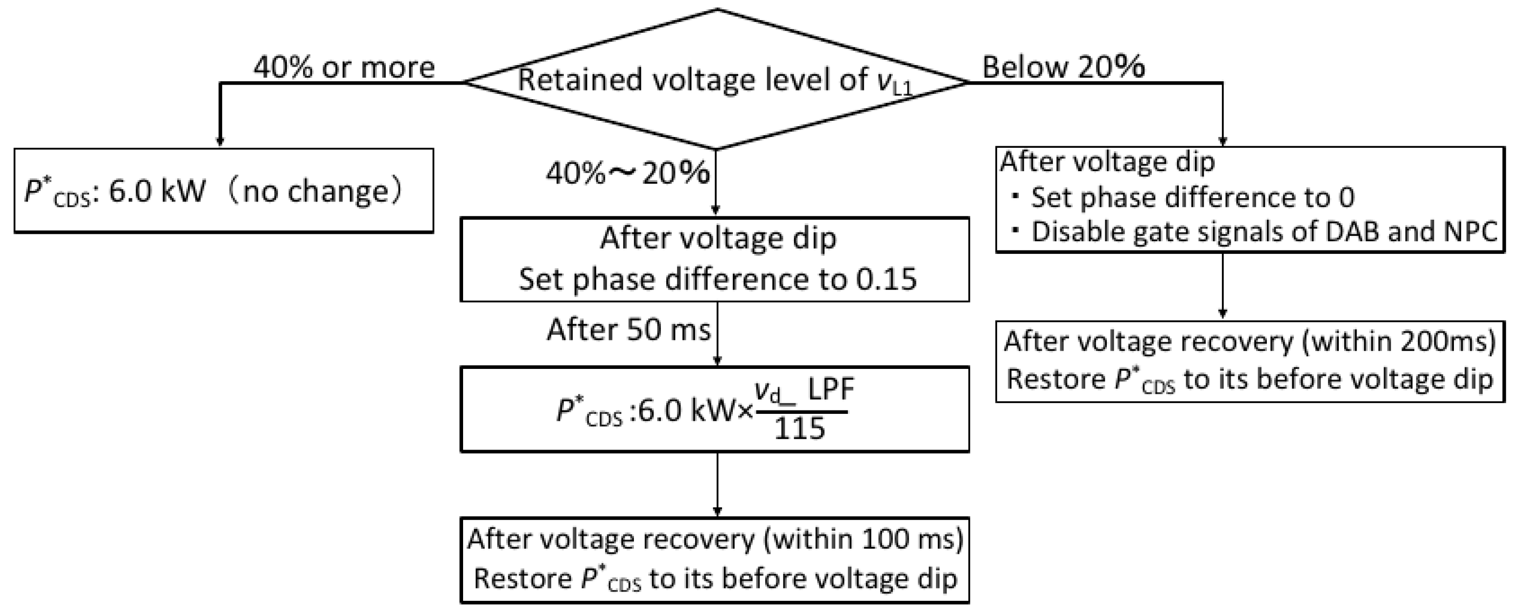
. When the retained voltage exceeds 40%, is between 20% and 40%, or reduces below 20%, the control logic branches to set an appropriate power reference. The step-by-step flow of this control process is illustrated in
Figure 8. It provides a clear representation of the manner in which
is determined based on the retained voltage. If the retained voltage is higher than 40%,
is maintained at 6.0 kW. This ensures full power delivery while maintaining the inverter current within the permissible range. When the retained voltage is in the intermediate range (20–40%), the control logic initially fixes the phase shift to 0.15 for 50 ms, corresponding to approximately 20% of the rated power output. This prevents current overshoot and provides a stable response during the early stage of the voltage dip. After this delay,
is expressed as follows:
This equation calculates the maximum permissible power required to ensure that the inverter output current does not exceed 75 Arms. The denominator 115 in Equation (
3) represents the peak voltage at 40% of the rated RMS grid voltage. This value is used as the threshold. When the retained voltage is below this level, the output power should be reduced to prevent exceeding the rated current of the inverter. By scaling the power reference proportionally to the detected peak voltage with respect to this 40% reference, the output current remains within the rated limit (75 Arms) even if the retained voltage reduces to 20%. This approach enables the system to maintain grid power balance while respecting the current limitation of the switching devices. When the voltage recovers, the output power reference returns to its pre-fault value within 100 ms. This satisfies the FRT requirement. If the retained voltage reduces below 20%, the system suspends the power delivery entirely by setting the phase shift to zero and disabling the gate signals for both NPC inverter and DAB converter. This measure prevents an excessive increase in the capacitor voltage
. When the voltage recovers, the output power reference returns to its pre-fault value within 200 ms, thereby satisfying the FRT requirement. This logic ensures that the power delivery is curtailed appropriately under each voltage condition. This effectively prevents device overcurrent while fulfilling the grid FRT criteria. After the appropriate reference power is selected, the PI controller regulates the phase shift command of the DAB converter to ensure that the instantaneous power
monitors the reference value. In this manner, the control system dynamically adjusts the power delivery based on the instantaneous grid voltage while maintaining the output current within the safe operating range of the inverter. This ensures compliance with the FRT requirements.
4. Simulation Results
A computer simulation was implemented using Altair PSIM software to validate the effectiveness of the proposed output power control method for FRT in a single-phase NPC inverter-based PCS with an IPOS DAB converter and DC power source. The topology followed the configurations described in
Section 2. To ensure the practical relevance of the simulation, the system configuration and control parameters were designed based on an actual experimental setup. In addition, the control and switching periods are the same to demonstrate the discrete performance of a digital controller in the experimental setup.
Table 2 summarizes the key parameters used in the proposed PCS simulation. The PCS is designed for a rated output power of 6.0 kW, which is typical for residential-scale systems. The switching frequency was set to 20.4 kHz, which is slightly above the audible range to ensure silent operation in residential environments. Moreover, this frequency allows the
-delay block used in the inverter control to be implemented with an integer number of samples. Specifically, to achieve an exact 90° phase shift, the switching frequency must be an integer multiple of four times the grid fundamental frequency. Therefore, 20.4 kHz was selected instead of 20 kHz because it is exactly divisible by 60 Hz. Accordingly, the external inductance was selected based on the rated output specifications. Therefore, the external inductance
was determined to ensure that the DAB converter could provide a rated power of 6.0 kW under the maximum phase shift condition. The maximum transferable power
of the DAB converter can be expressed as follows:
where
and
denote the voltages of the DAB’s primary side (connected to the DC power source) and secondary side (connected to the NPC inverter), respectively.
is the angular frequency corresponding to the switching frequency
.
is the external inductance between the transformer and converter legs. The value of
is thus selected to ensure a rated power delivery of 6.0 kW when operating under the maximum phase shift condition of
. Substituting the rated voltages and switching frequencies into Equation (
4), the external inductance is sized appropriately to satisfy the power delivery requirements of the system.
Following the design of the external inductance, the DC-link capacitor values were determined to suppress the voltage ripple resulting from power oscillations at two times the grid frequency. Assuming that the inverter output current is controlled at a power factor of 1.0 and that the grid voltage is a sinusoidal waveform, the instantaneous output power of the grid-tied inverter
can be expressed as follows:
The second term in (
5) represents the power ripple component at two times the grid frequency. It causes a voltage ripple across the DC-link capacitor. In the following discussion, this ripple component is denoted as
. To limit the resulting voltage ripple to within 5% of the steady-state average DC voltage, the required capacitor size is determined such that the energy fluctuation induced by
can be absorbed sufficiently [
26]. The permissible energy fluctuation within the voltage limits
and
is given by:
Equating
to
, the minimum capacitance required to maintain the target ripple constraint can be expressed as follows:
Substituting the rated grid voltage
, inverter current
, and ±5% ripple tolerance, the minimum required capacitance for each half of the split capacitor is calculated as
. It should be noted that this value represents the theoretical minimum required to satisfy the ripple constraint. In the actual implementation, approximately two times this capacitance is adopted to provide an additional design margin and improve the system reliability. The selected values of
and
listed, in
Table 2, were adopted in the subsequent simulation and evaluation by referring to this design principle. Detailed device characteristics were incorporated into the simulation model to realistically evaluate the power losses and switching behavior. The NPC inverter employs Si-MOSFETs (IXYS, IXFK150N30P3) as switching elements. Each device has a drain–source voltage rating of 300 V, a maximum continuous drain current of 150 A, an on-state resistance of 19 mΩ, and a forward voltage drop of 1.5 V for the body diode. The primary-side full-bridge of the DAB converter uses Si-MOSFETs (IXYS, IXFR180N15P) rated at 150 V, with a maximum continuous drain current of 100 A, an on-state resistance of 13 mΩ, and a body diode forward voltage drop of 1.5 V. The secondary-side full-bridge of the DAB converter has device specifications identical to those of the NPC inverter and employs an IXFK150N30P3. Furthermore, the efficiency evaluation in this section was conducted using detailed device parameters to realistically represent the steady-state power losses. In particular, both the on-state resistance and body-diode forward voltage drop of the Si-MOSFETs were incorporated into the PSIM model, allowing the simulated efficiency to closely approximate the practical operating conditions. Although the switching losses can be modeled in PSIM, they were not included in this system. Therefore, the efficiency analysis focuses on steady-state conduction losses, which can be accurately evaluated using the actual device parameters. Despite this limitation, the obtained results still provide a reliable estimation of the steady-state efficiency and sufficiently demonstrate the practical effectiveness of the proposed control method. In addition, the DAB converter employs an ideal transformer with a turns ratio of 1:2 (primary to secondary). Herein, zero core loss or leakage inductance is assumed. The following section presents the simulation waveforms and power flow characteristics under normal and fault conditions. The FRT performance was evaluated based on Japan’s FRT requirements.
4.1. Simulation Results Under Normal Grid Voltage Conditions
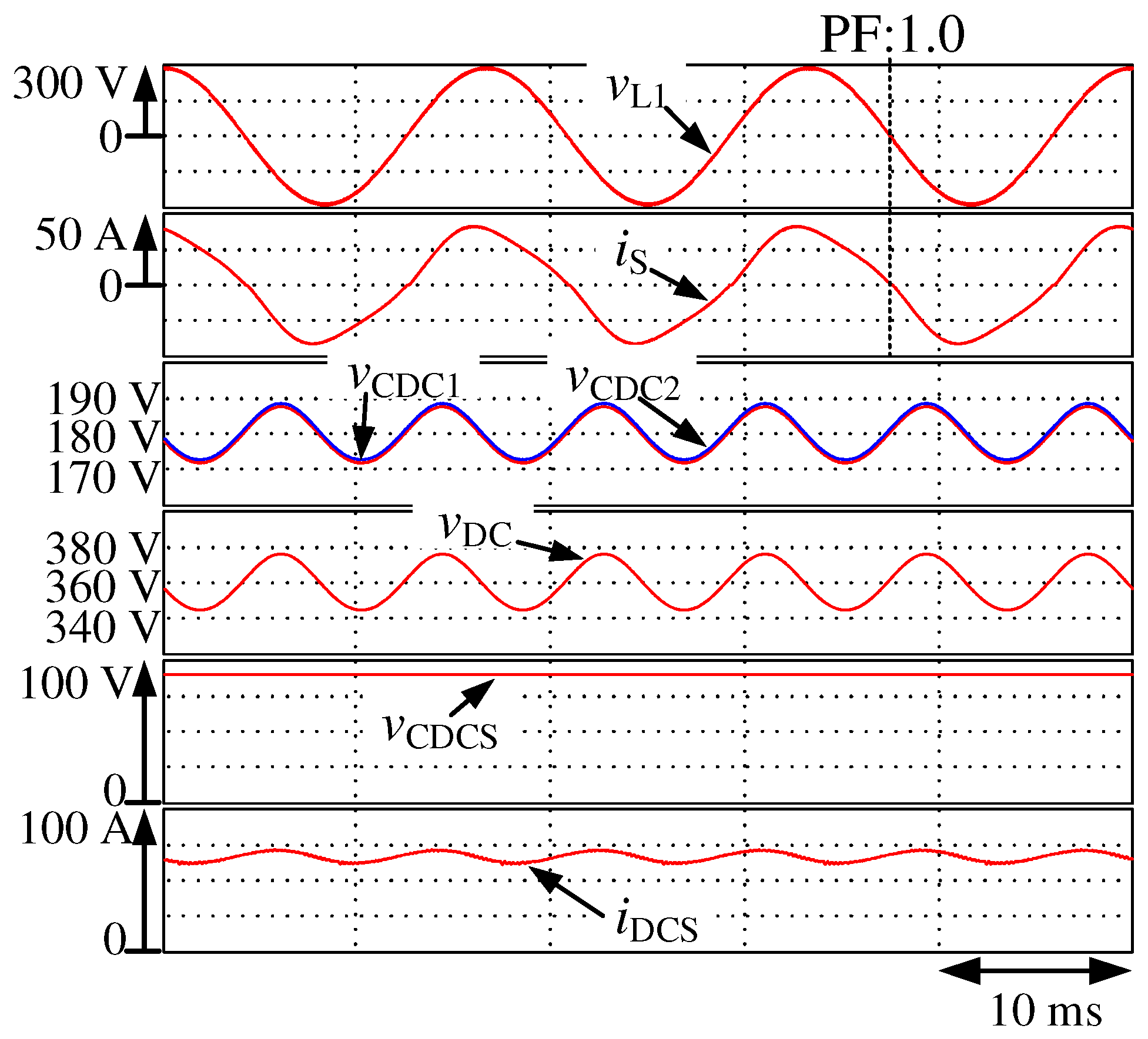
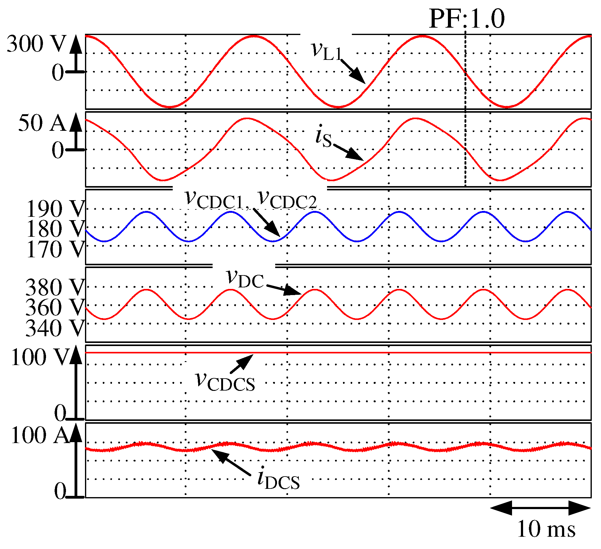
Figure 9 shows the simulation waveforms under normal grid voltage conditions, where the system provides a rated output power of 6.0 kW from the DC voltage source to the utility grid. At the top of
Figure 9,
is the grid voltage,
is the source current,
and
are the capacitor voltages,
is the DC-link voltage,
is the battery voltage, and
is the battery current. The current
is a sinusoidal waveform with a unity power factor. Thus, the proposed PCS can inject active power from a battery. The capacitor voltages
and
are well balanced. This implies that the midpoint potential was stabilized. The DC-link voltage
was maintained at approximately 360 V, and the voltage ripple was within 5%. This satisfied the design target. The DAB converter transmitted 6.0 kW from the battery to the DC-link capacitor. The power injected from the DC-link into the grid was approximately 5.71 kW.
Battery current
includes a low-frequency component. This component originates from the second-order ripple of the DC-link side voltage of the DAB converter, which fluctuates at twice the grid frequency due to the power pulsation associated with AC power transfer. In addition, a comparative analysis was performed to validate the difference in the power conversion efficiency between the conventional DAB converter and the IPOS-DAB converters. The conventional DAB converter was simulated under identical conditions. The exception was that the secondary-side MOSFETs of the DAB were replaced with Si-MOSFETs (TOSHIBA, TK100L60W, VQ). In this device, the rated voltage is 600 V, the maximum continuous drain current is 101 A, the on-state resistance is 15 mΩ, and the forward voltage drop of the body diode is 1.7 V. Similar to the case of the IPOS-DAB, the steady-state conduction losses were modeled accurately. An ideal transformer was used in the DAB converter to verify the basic operation of the proposed system. The winding turn ratio of the transformer was set to 1:4.
Figure 10 shows the simulation waveforms under normal grid voltage conditions. Here, the conventional DAB converter system provides a rated output power of 6.0 kW from the DC voltage source to the utility grid. Similar to the IPOS-DAB system, the inverter operates with a unity power factor. Thereby, it achieves a successful reverse power flow to the grid. The output power of the DC voltage source is 6.0 kW. The power injected into the grid is approximately 5.69 kW.
Table 3 summarizes the power flow comparisons between the two configurations. The IPOS-DAB converter achieved a higher efficiency of 95.2%, whereas the conventional DAB converter achieved 93.8%. This corresponds to a 1.4% gain in efficiency. The result agrees well with those of previous studies [
19,
20] and further supports the advantage of the IPOS configuration. Given that ideal transformers were assumed, the actual efficiency difference is likely to widen in practical implementations, where the transformer core and copper losses become significant. These observations reinforce the suitability of the proposed PCS architecture that combines the NPC inverter and IPOS-DAB converter as a high-efficiency solution for residential applications.
To reduce the current ripple on the primary side of the DAB converter, the proposed system employs the interleaved operation of two DAB converters. This is described in
Section 2.
Figure 11 shows the simulated current waveforms under this interleaving scheme. The top two waveforms represent the primary currents
and
of the two interleaved DAB converters. The third waveform from the top is the combined current
. It exhibits a significantly reduced ripple amplitude compared with the case in which the individual DAB currents are combined without a phase shift. In particular, the ripple frequency of the combined current increases to twice the switching frequency of each DAB, which effectively shifts the dominant ripple component to a higher frequency. This frequency doubling allows the LC filter to achieve the same attenuation performance with a smaller inductance value. For the present LC filter parameters (
= 24
H,
= 47
F), the cutoff frequency is approximately 4.7 kHz, corresponding to about 1/20 of the 80 kHz ripple frequency. If the same attenuation were required for the 40 kHz ripple observed in a conventional single-DAB configuration, the cutoff frequency would need to be lowered to about 2.4 kHz, which would require an inductance of approximately 90
H (≈3.8 times larger). According to the magnetic design principle based on the area-product method [
27], the inductor volume and cost are roughly proportional to
. Therefore, increasing
L by a factor of about 3.8 would lead to a similar increase in inductor volume and cost under the same current and thermal conditions. For practical magnetic design, an amorphous core material was assumed with a peak current of 70 A and a conductor cross section of
. The allowable flux density was set to approximately half of the saturation flux density of the amorphous material to ensure sufficient magnetic margin. Under these conditions, the 24
H inductor can be realized using a CS-6.3 core with 12 turns, whereas the 90
H inductor requires a CS-32 core with 22 turns.
Figure 12 shows the dimensions of the cut cores used for the magnetic design: (a) CS-6.3 and (b) CS-32. The core volume of the latter is approximately three times larger, confirming the effectiveness of the proposed interleaved IPOS-DAB configuration in reducing the inductor size and cost. Consequently, the proposed interleaved configuration enables significant system miniaturization and cost reduction while maintaining equivalent filtering performance. The bottom waveform shows the output current
after passing through an LC filter. The result verify that the interleaved operation effectively suppresses high-frequency ripple components.
4.2. Simulation Results Under 20% Voltage Dip Conditions
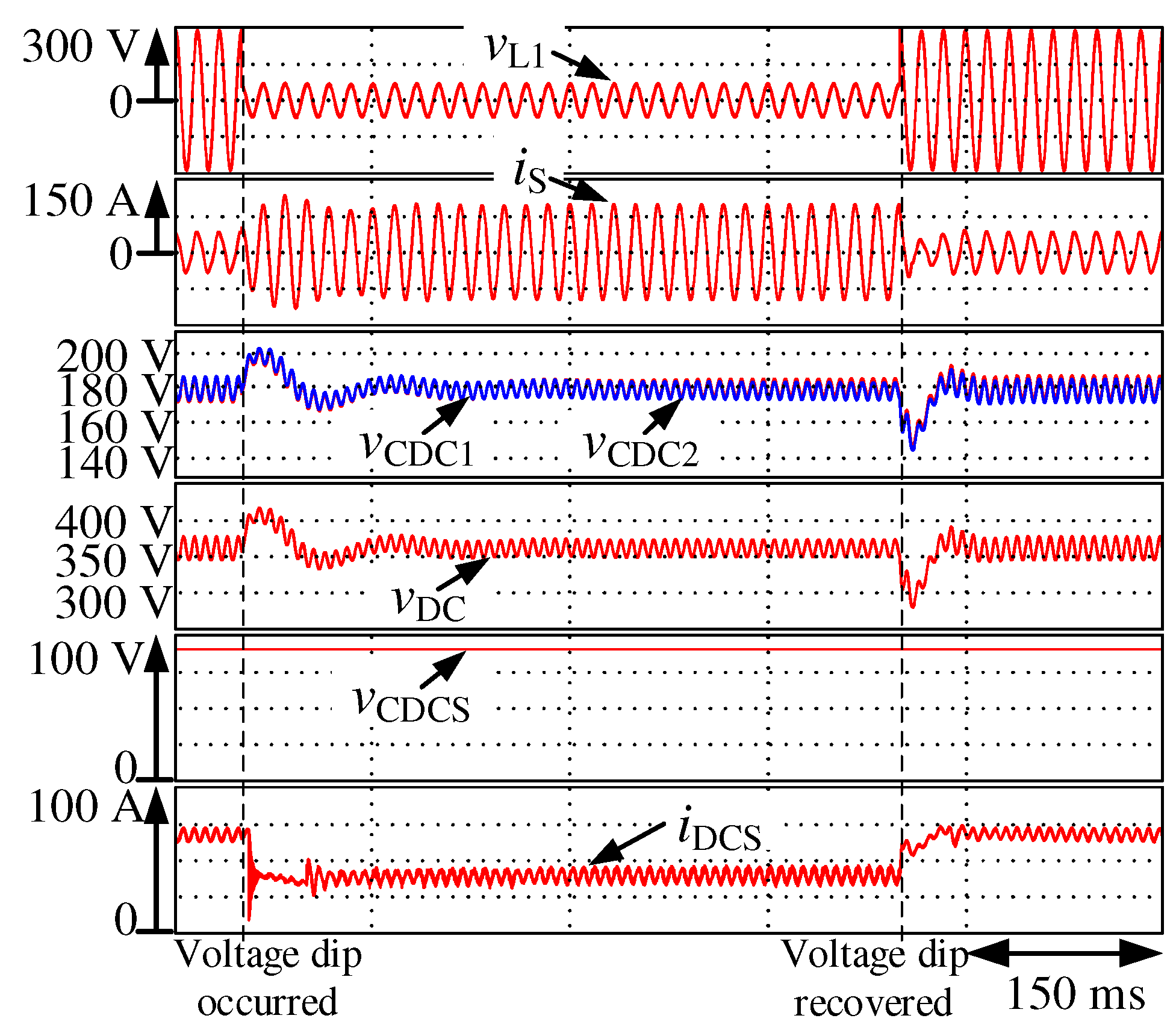
Figure 13 shows the simulation waveforms during a dip to 20% of the nominal grid voltage when the PCS provides a rated power of 6.0 kW. The duration of the voltage dip is 500 ms. According to the control flow chart in
Figure 8, when the retained voltage
falls within the 20–40% range, the output power of the DAB converter reduces smoothly. This adjustment effectively prevents overcurrent, as described in
Section 3. Notwithstanding the substantial voltage reduction, the steady-state value of
is maintained at approximately 75 Arms. The value corresponds to the upper current limit determined by the safe operating area of the switching device. This indicates that the proposed output power control strategy effectively prevents overcurrent by regulating the current within a safe range during the fault. The capacitor voltages
and
remain well-balanced. This indicates a stable midpoint potential even during the voltage dip. The DC-link voltage
exhibits a temporary fluctuation. However, it recovers rapidly after the fault is cleared. The bottom two waveforms show the output voltage
and current
of the DC source. The DAB converter continues to extract power from the DC power source without interruption.
Table 4 summarizes the power flow transitions corresponding to
Figure 13. It compares the system states before, during, and after the voltage dip. During the voltage dip period, both DAB output power and reverse power flow to the grid decrease in accordance with the retained voltage and implemented power control strategy. According to the Japanese FRT requirements, for voltage dips with at least 20% retained voltages, the output power should recover to its pre-fault level within 100 ms. The power recovery time is measured as the interval between the instant of voltage restoration and the time when the reverse power flow exceeds 80% of its pre-fault value. In the present case, recovery is achieved within 20 ms, thereby effectively satisfying this requirement. These results verify that the proposed system satisfies the Japanese FRT requirements with a sufficient margin. Additionally, it ensures stable and grid-supportive operation even under severe voltage dip conditions.
4.3. Simulation Results Under 0% Voltage Dip Conditions
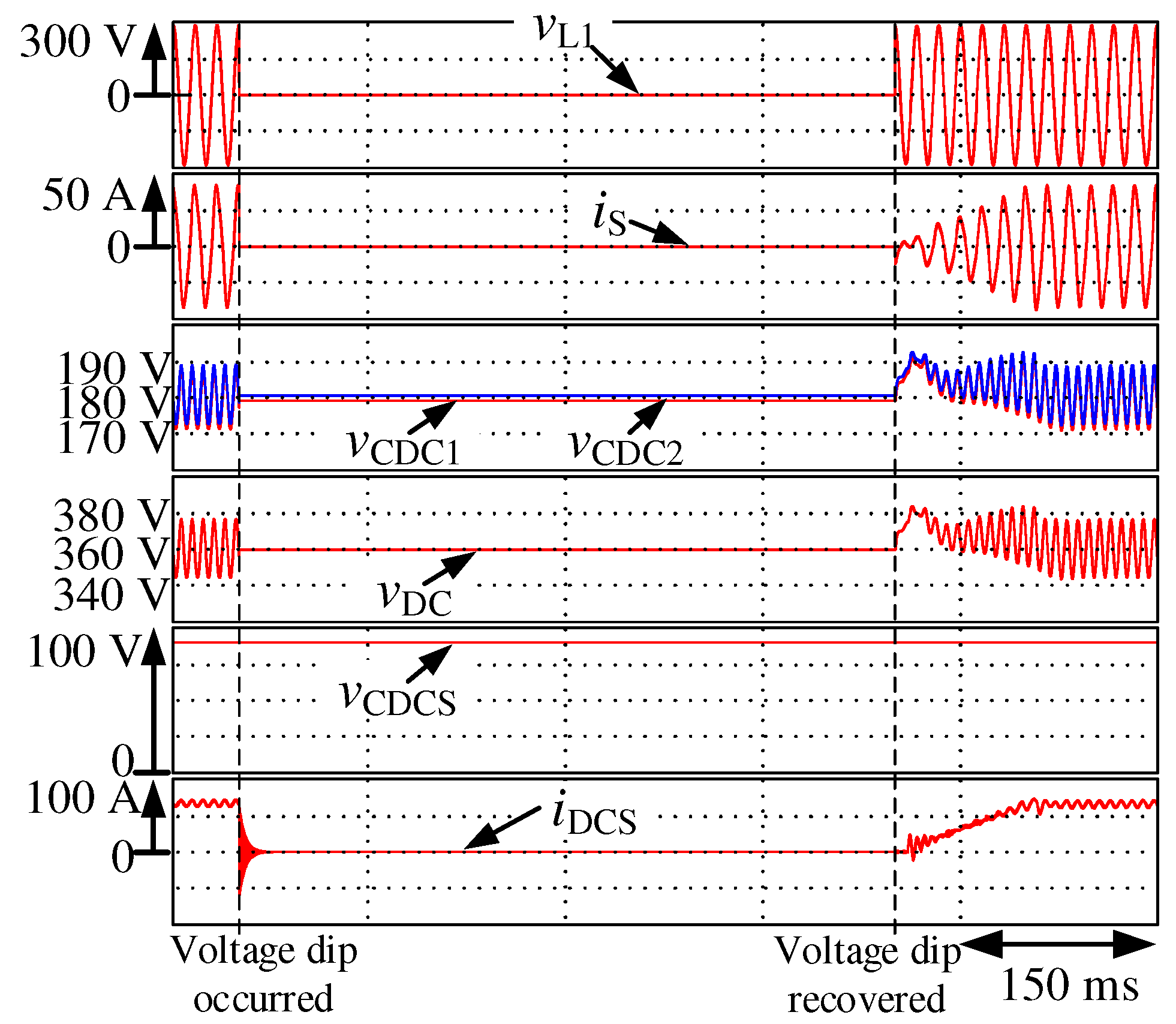
Figure 14 shows the simulation waveforms during a grid voltage dip to 0% of its nominal value. This occurs when the PCS provides a rated power of 6.0 kW. The duration of the voltage dip duration is 500 ms. According to the control flow shown in
Figure 8, when the retained voltage
falls below 20%, the output power reference of the DAB converter is set to zero, all the switching devices are turned off, and the power transfer is suspended to prevent reverse current injection into the grid and protect the system. This is described in
Section 3. The grid voltage
, simulates the voltage dip. It reduces abruptly to 0 V and recovers after 500 ms. As a result of the control, source current
becomes zero during the fault. This verifies that no current is injected into the grid under the zero-voltage condition.
Table 5 summarizes the power flow transitions corresponding to this simulation. It also compares the system states before, during, and after the voltage dip. During the fault, both DAB output power and reverse power flow to the grid reduce to 0.00 kW. This demonstrates that the power transfer is suspended completely in accordance with the control strategy. After the fault is cleared, the output power recovers to over 80% of the pre-fault value within approximately 90 ms. The power recovery time is measured as the interval between the instant of voltage restoration and the time when the reverse power flow exceeds 80% of its pre-fault value. This satisfies the Japanese FRT requirement, which stipulates that output power should recover to at least 80% of the pre-fault level within 200 ms of voltage recovery. These results demonstrate that the proposed system effectively prevents reverse current injection during this fault scenario and rapidly resumes power delivery in compliance with the FRT requirements.
5. Conclusions
This paper proposes an output power control method for FRT in a single-phase NPC inverter-based PCS composed of an IPOS DAB converter and battery. The proposed PCS can inject battery power within the limits of the output current of the NPC inverter-based PCS when voltage disturbances occur. A computer simulation was implemented to verify the validity of the proposed system using Altair PSIM software. To ensure the practicality of the proposed control method, the simulation model was developed using the same configuration and control parameters as those intended for the experimental setup. Furthermore, the control and switching periods were the same to demonstrate the discrete performance of a digital controller in the experimental setup. Under normal grid conditions, the system achieved an efficient reverse power flow at a rated output of 6.0 kW. Compared with a conventional DAB converter configuration, the proposed IPOS-DAB converter improved the conversion efficiency by 1.4%. Under grid fault conditions, the output power control strategy was verified to comply with the Japanese FRT requirements. During a 20% voltage dip, the system maintained the output current within the safe operating range of the device while delivering the maximum permissible power. Power recovery was achieved within 20 ms. During a 0% voltage dip, power transfer was suspended to prevent reverse current injection, and resumed within 90 ms after fault clearance. This satisfied the 200 ms recovery requirement. Therefore, the proposed PCS architecture provides both high efficiency and reliable FRT capability. This makes it a strong candidate for residential energy systems requiring stable grid interaction. In future work, we will construct the experimental setup and test the practicability of the proposed control method.


