Article

CISC-YOLO: A Lightweight Network for Micron-Level Defect Detection on Wafers via Efficient Cross-Scale Feature Fusion

School of Mechanical Engineering, University of Shanghai for Science and Technology, Shanghai 200093, China
*
Author to whom correspondence should be addressed.
Electronics 2025, 14(19), 3960; https://doi.org/10.3390/electronics14193960
Submission received: 1 September 2025 / Revised: 21 September 2025 / Accepted: 25 September 2025 / Published: 9 October 2025

Abstract

With the development of the semiconductor manufacturing process towards miniaturization and high integration, the detection of microscopic defects on wafer surfaces faces the challenge of balancing precision and efficiency. Therefore, this study proposes a lightweight inspection model based on the YOLOv8 framework, aiming to achieve an optimal balance between inspection accuracy, model complexity, and inference speed. First, we design a novel lightweight module called IRB-GhostConv-C2f (IGC) to replace the C2f module in the backbone, thereby significantly minimizing redundant feature computations. Second, a CNN-based cross-scale feature fusion neck network, the CCFF-ISC neck, is proposed to reduce the redundant computation of low-level features and enhance the expression of multi-scale semantic information. Meanwhile, the novel IRB-SCSA-C2f (ISC) module replaces the C2f in the neck to further improve the efficiency of feature fusion. In addition, a novel dynamic head network, DyHeadv3, is integrated into the head structure, aiming to improve the small-scale target detection performance by dynamically adjusting the feature interaction mechanism. Finally, so as to comprehensively assess the proposed algorithm’s performance, an industrial dataset of wafer defects, WSDD, is constructed, which covers “broken edges”, “scratches”, “oil pollution”, and “minor defects”. The experimental results demonstrate that the CISC-YOLO model attains an mAP50 of 93.7%, and the parameter amount is reduced to 1.92 M, outperforming other mainstream leading algorithms in the field. The proposed approach provides a high-precision and low-latency real-time defect detection solution for semiconductor industry scenarios.

1. Introduction

Integrated circuit (IC) chips, as the core components of modern electronic devices [1], are constructed on semiconductor wafers via complex processes, including photolithography, etching, and deposition. Semiconductor wafers, as the basic substrates for IC manufacturing, form dense microcircuit structures through extremely precise processes. With the continuous advancement of semiconductor technology, wafer fabrication is gradually moving toward higher integration and miniaturization [2], allowing billions of nanoscale electronic components to be integrated into a single wafer. However, complex fabrication environments and processes inevitably introduce surface defects such as scratches, pits, broken edges, chemical stains, and dust contamination. These unanticipated structural defects may cause circuit performance degradation and lead to significant yield degradation through the formation of a gross failure area. Especially when defects are not detected in time, even minor anomalies can be amplified in subsequent processing, resulting in production cost surges, yield fluctuations, and a decline in process stability. Therefore, real-time and high-precision defect detection is essential to ensure chip reliability and optimize production efficiency and has become a strategic priority for the semiconductor industry [3].
Early defect detection methods for semiconductor wafer surface defects mainly relied on experienced operators to identify the defects through optical microscopes or the naked eye, which carried the drawbacks of inefficiency, low accuracy, excessive workforce demands, and high cost. To overcome these limitations, machine learning-based [4,5] defect detection methods have gained prominence in wafer inspection. For example, Yuan et al. [6] proposed a K-nearest neighbor (KNN) denoising technique to efficiently identify spatial defect patterns on wafers through a similarity-based clustering method combined with a model selection criterion. Gómez-Sirvent et al. [7] designed an exhaustive search (ES)-optimized feature selection framework to augment the predictive capabilities of support vector machine (SVM) classifiers in detecting wafer surface defects. Xie et al. [8] established an SVM classification framework for the systematic detection of morphological defects in semiconductor wafer production lines, which performs well in dealing with high-dimensional data and multiple defect patterns. However, these approaches often suffer from computational complexity, compromised detection accuracy, high latency, and poor cross-scenario adaptability in complex industrial scenarios, thus failing to meet industrial real-time detection demands.
In recent years, deep learning [9,10] inspection techniques embodied by convolutional neural networks (CNNs) have emerged as the mainstream solutions for defect detection in semiconductor manufacturing processes due to the advantages of their non-contact nature, high-speed automation, low cost, and high accuracy. Two-stage detectors like Faster R-CNN [11], region-based fully convolutional networks (R-FCN) [12], and Mask R-CNN [13] achieve high accuracy. Zhuang et al. [14] integrated an FPN into the feature extraction part of Faster R-CNN, generating multi-scale feature pyramids through bottom-up and top-down paths and employing ResNet-50 for characteristic extraction, thus solving the problem of small target missed detection caused by discarding low-level features in traditional Faster R-CNN. Wu et al. [15] presented a welding point defect detection approach built upon Mask R-CNN, which utilizes ResNet-101 as the backbone network for image feature extraction, and the method significantly reduces the probability of misdetection in the stage of electronic packaging. These algorithms show high accuracy and robustness in dealing with complex defects. However, their substantial numbers of model parameters, slow inference speeds, and significant computational overhead make them insufficient to meet the demand for rapid detection in semiconductor production lines.
In contrast, single-stage detectors, especially the You Only Look Once (YOLO) series [16], strike a balance between speed and accuracy by segmenting the captured image into a grid and directly predicting the bounding box and category probabilities. With the advantages of high speed, high accuracy, and low GPU consumption, the YOLO series has enabled significant advances in medium and large target detection in the industrial sector [17]. For example, Shinde et al. [18] demonstrated the excellent performance of detection networks such as YOLOv3 and YOLOv4 for wafer defect localization and classification, where the YOLO series achieved 94% classification accuracy. Tao et al. [19] proposed a wafer inspection network based on YOLOv8 and validated it on the WM-811K dataset. With high accuracy and computational efficiency, the network outperformed the single-shot multi-box detector (SSD) [20] and YOLOv5. Some researchers have focused on integrating attention mechanisms into the YOLO architecture to enhance key features and improve the accuracy of the model. For example, Wang et al. [21] introduced a spatial attention module (SAM) in the YOLOv4 backbone network to improve the detection capabilities of the model for tiny defects on wafers. Li et al. [22] employed the ECA attention mechanism to enhance the C2f module of the YOLOv5 backbone and necking network, thereby augmenting the model’s capacity to localize defects by dynamically emphasizing key features in the channel dimension. To address the challenges of small-scale target detection, some researchers have proposed various improvements by enhancing the detection head designs of YOLO networks. Zhou et al. [23] incorporated an innovative minor object detection layer (SODL) into the head network of YOLOv7, employing upsampling and feature fusion to produce high-resolution feature maps and refine the anchor frame size. Experimental results demonstrate that this approach enhances the AP50 for small-scale targets by up to 5.6%. Wang et al. [24] developed the YOLOv8-QSD model, which adds a new Q-block based on replacing the traditional prediction head with a DyHead to enhance the localization accuracy of small targets by relocating the shallow features of the p2 layer to compensate for the loss of information in the downsampling process. Although the above methods have shown significant progress in specific tasks, their performance improvement relies on complex modular designs, leading to a significant increase in computational complexity. In addition, the problems of leakage and misdetection due to the tiny sizes of wafer defects and the complex background conditions are still not completely resolved.
To address the aforementioned issues, this study proposes a lightweight model, CISC-YOLO, which is able to improve the performance of wafer detection with low hardware resource consumption, thereby fulfilling the application demands for real-time target detection in the industrial field. In this model, ghost convolution (GhostConv) is introduced into the backbone network to decrease the computational complexity while preserving the feature information integrity. Secondly, a novel neck structure, CCFF-IRB-SCSA-C2f (CCFF-ISC), is proposed to enhance the efficiency of cross-scale feature fusion, ensuring a high inference speed while strengthening the correlation between cross-level features via the ISC module, thereby enhancing the model’s ability to focus on multi-scale features. Finally, a novel dynamic detection head called DyHeadv3 is designed by combining deformable convolutional networks v3 (DCNv3), which enables adaptive feature optimization across layers and significantly improves the accuracy of sub-micron defect localization. Through the synergistic optimization of the above modules, this work effectively compresses the size of the model and achieves a balance between accuracy and speed.
(1)
We propose a lightweight IRB-GhostConv-C2f (IGC) module based on ghost bottlenecks. It reduces redundant computations in the backbone network by separating intrinsic feature generation and decoupling it from linear transformations, providing an efficient solution for real-time detection at the edge.
(2)
A CNN-based cross-scale feature fusion (CCFF) necking network, the CCFF-ISC neck, is proposed. It employs lightweight 1 × 1 convolution and a dual-path interaction mechanism, and also employs the IRB-SCSA-C2f (ISC) module instead of the traditional C2f module, to improve the feature fusion efficiency and reduce parameter redundancy.
(3)
This article proposes a new DyHeadv3 to replace the original head network. By leveraging the synergistic effects of the dynamic head (DyHead) and DCNv3, the proposed model enhances the semantic representation of high-level features while enriching the details of low-level features. Furthermore, the proposed dynamic detection head effectively mitigates the performance degradation typically associated with static detection heads in industrial environments, where geometric variations and background interference are prevalent.
(4)
We construct a wafer surface defect dataset (WSDD) in a real industrial environment and scale it up to 3256 images for model evaluation using data enhancement techniques, demonstrating the effectiveness of the proposed architecture.

2. Methods

Section 2 details the architectural design and core improvement strategy of the proposed lightweight wafer defect detection model, CISC-YOLO. As depicted in Figure 1, the model is built upon the YOLOv8 framework, and the synergistic enhancement of accuracy and efficiency is achieved through the lightweight reconstruction of the backbone network, cross-scale feature fusion optimization, and the dynamic design of the detection head. Specific improvements include the incorporation of the IGC module within the backbone network, the adoption of the CCFF-ISC structure for the neck network, and the implementation of the DyHeadv3 architecture for the detection head part.

2.1. Lightweight Backbone Network

The backbone network of YOLOv8 is predominantly responsible for feature extraction, which is achieved by stacking many conventional convolutional layers. Although conventional CNNs exhibit strong performance in feature extraction and and contextual information transfer, their high parameter density and computational redundancy severely limit the deployment efficiency in edge devices. GhostConv is introduced in the backbone network to decrease redundant computations and the parameter quantity. The operation principles of traditional convolution and ghost convolution are shown in Figure 2.
Given an input X R c × h × w , the output Y R n × h × w corresponding to the nth channel in a conventional convolutional is mathematically expressed as:
Y = X f + b ( f R c × k × k × n )
where f represents the convolutional kernel tensor, b denotes the bias term, and k × k denotes the size of the convolutional kernel. The computational cost of this process is O ( n · c · k 2 · h · w ) , leading to a significant computational burden when n is large.
To resolve the redundancy issue in the output feature maps in Equation (1), the bias term b is removed, and a reduced convolutional kernel is used to generate m = n / s feature maps Y R m × h × w .
Y = X f ( f R c × k × k × m )
where m n , and the rest of the parameters are kept consistent with Equation (1). To more effectively acquire the required n feature maps, a cheap linear transformation C i , j ( · ) is applied to every raw feature map y i Y , leading to the creation of s ghost feature maps:
y i j = C i , j ( y i ) , i = 1 , . . . , m , j = 1 , . . . , s ,
The final output is operated via channel splicing:
Y = Concat ( Y , Y ˜ )
where Y ˜ = { y ˜ i , j } denotes the set consisting of all ghost feature maps y ˜ i , j , and the number of output channels n = m · s satisfies Y R n × h × w .
Inspired by MobileNetV2 [25], we replace the bottleneck structure in the C2f module of the backbone network with the IG-Bottleneck module, designed with an inverted residual block (IRB), as illustrated in Figure 1. This initially doubles the input channel dimension through GhostConv and then maps the low-dimensional features into the high-dimensional space to enhance the expression capabilities of subsequent operations. It then employs depthwise convolution (DWConv) using a stride of 2 to significantly reduce the computational complexity while maintaining the ability to extract localized spatial features. Finally, GhostConv dimensionality reduction recovers the original number of channels, and residual connectivity is introduced to avoid global information loss. The IGC module simultaneously preserves high accuracy while reducing the computational overhead.

2.2. CCFF-ISC Neck Network

YOLOv8’s neck utilizes a path aggregation network (PANet) structure to perform multi-scale feature fusion. The traditional PANet performs feature fusion via top-down and bottom-up routes, but this approach suffers from computational redundancy or insufficient efficiency. To further optimize the model’s volume and number of parameters, as shown in Figure 1, this study proposes a more efficient CCFF-ISC necking network, which is synergistically optimized by the lightweight module design and the attention mechanism, guaranteeing efficient feature fusion and a lower computational load.
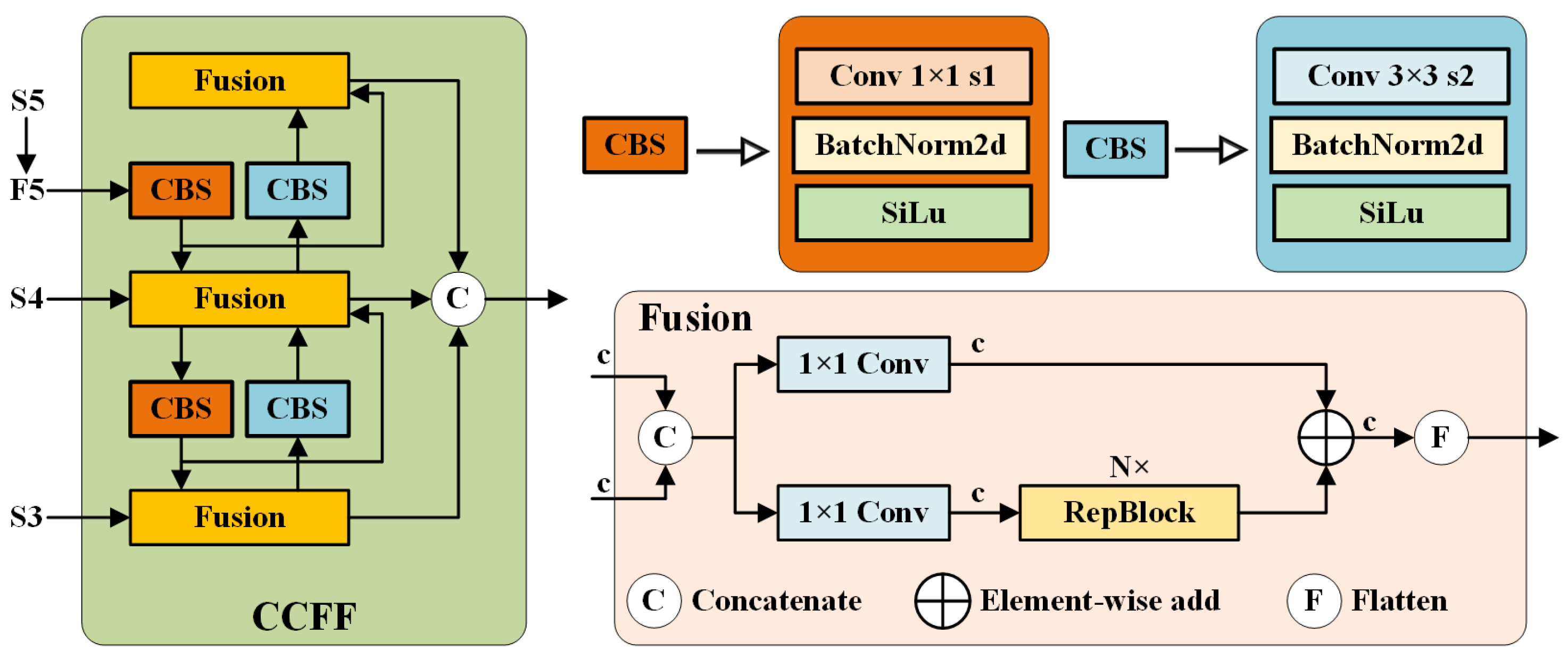
Refer to Figure 3 for the CCFF structure’s treatment of the F5 layer. We apply 1 × 1 convolution to the output feature maps of SPPF in the YOLOv8 model to reduce the number of channels of the output feature maps from 1024 to 256 while keeping the input dimensions unchanged. This reduces the model’s parameter count and achieves the linear combination of the information between the channels, facilitating cross-channel interaction. In addition, further drawing on CCFF’s treatment of S3 and S4, we perform 1 × 1 convolutional dimensionality reduction on the output features of layers 4 and 6 of the YOLOv8 model’s backbone network and fuse them with the processed features at other scales. Finally, the deep feature map is combined with the feature map after upsampling. This cross-layer connection design not only expands the model’s perceptual scope but also allows it to utilize both high-resolution details and low-resolution semantics, thereby enabling multi-scale adaptability for wafer defect recognition.
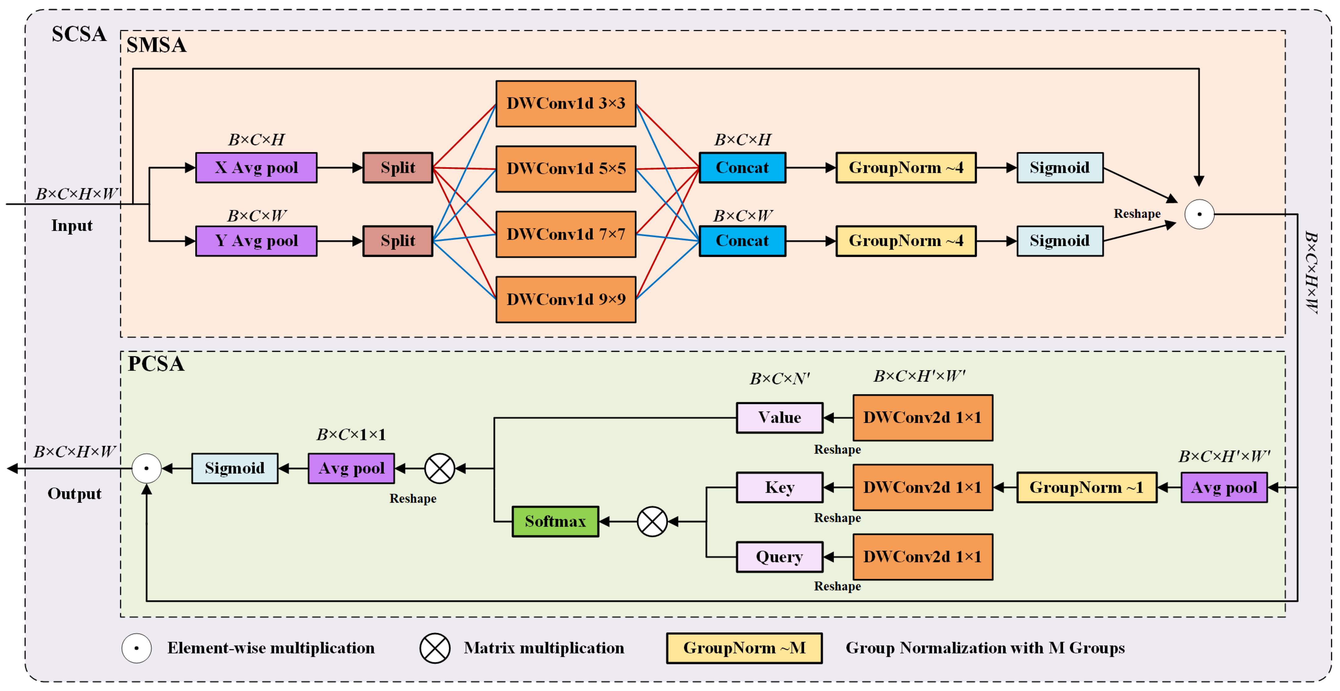
In addition, to further strengthen the model’s feature expression and elevate its performance in industrial defect detection, we introduce a lightweight and practical spatial and channel synergistic attention (SCSA) [26] module in the above-improved neck part. The SCSA module enhances feature expression through the synergy between shareable multi-semantic spatial attention (SMSA) and progressive channel-wise self-attention (PCSA), as shown in Figure 4. Given the input X R B × C × H × W , SMSA decomposes the input feature into K independent sub-features along the height (H) and width (W) dimensions X H R B × C × H and X W R B × C × H . Then, 1D DWConv is employed to capture spatial structural information across various semantic layers. Next, convolution kernels of various scales (3, 5, 7, and 9) are applied to each sub-feature X H i and X W i .
X H i = X H [ : , ( i 1 ) × C K : i × C K , : ]
X W i = X W [ : , ( i 1 ) × C K : i × C K , : ]
X ˜ H i = D W C o n v 1 d k i C K C K ( X H i )
X ˜ w i = D W C o n v 1 d k i C K C K ( X W i )
where X i represents the ith sub-feature, i [ 1 , K ] . X ˜ i denotes the spatial structure information of the ith sub-feature acquired post-convolution, and k i is the convolution kernel utilized on the ith sub-feature. Then, the independence between sub-features is maintained by group normalization (GN). Finally, the spatial attention weights are derived from the sigmoid activation function, which focuses on detecting critical regions of the image. The output features are represented in the following equation:
A t t n H = σ ( G N H K ( C o n c a t ( X ˜ H 1 , X ˜ H 2 , , X ˜ H k ) ) ) A t t n W = σ ( G N w K ( C o n c a t ( X ˜ W 1 , X ˜ W 2 , , X ˜ W k ) ) ) S M S A ( X ) = X s = A t t n H × A t t n W × X
where σ · denotes the sigmoid normalization process; G N H K and G N W K denote GN with K groups in H and W dimensions, respectively.
The PCSA module gradually compresses the spatial dimensions through average pooling, which both preserves the spatial a priori information provided by SMSA and effectively reduces the computational complexity. Subsequently, the single-head channel self-attention mechanism performs similarity computation along the channel dimension, utilizing the spatial a priori information to direct the interaction between channel features and effectively mitigate the differences between the semantic information. The complete derivation formula is as follows:
X p = P o o l ( k , k ) ( H , W ) ( H , W ) ( X s )
F p r o j = D W C o n v 2 d ( 1 , 1 ) C C
Q = F p r o j Q ( X p ) , K = F p r o j K ( X p ) , V = F p r o j V ( X p )
X a t t n = Softmax Q K τ C V
P C S A ( X s ) = X c = X s × σ ( P o o l ( H , W ) ( H , W ) ( 1 , 1 ) ( X a t t n ) )
where P o o l ( k , k ) ( H , W ) ( H , W ) denotes reshaping ( H , W ) into ( H , W ) using a pooling operation with convolutional kernel size k. F p r o j ( · ) denotes the linear projection process. Finally, SCSA consists of two sub-modules, SMSA and PCSA, which are connected in series. The design effectively balances computational efficiency and accuracy.
S C S A ( X ) = P C S A ( S M S A ( X ) )
We design the efficient feature processing module ISC to introduce the neck network, which adopts a similar approach to the IGC module, fuses the design concepts of C2f and bottleneck modules, and combines the inverted residual structure with the SCSA attention module. The complete structure is explained in Figure 1. Compared with the traditional C2f module, ISC significantly decreases the parameter quantity and computations. Additionally, the SCSA attention module compensates for the deficiencies of deep convolution in terms of feature extraction capabilities compared to full convolution.

2.3. Head Network Structure of DyHeadv3

YOLOv8’s head network adopts a decoupled approach to directly predict category and bounding box coordinates through multiple regular convolutional layers. However, this approach leads to inaccurate localization when the target is deformed, occluded, or has unconventional viewpoints. In addition, sharing features for classification and regression tasks may lead to inter-task interference, which does not allow for the adequate fusion of semantic information across layers in complex industrial scenarios. To address this challenge, we first introduce DyHead [27], which dynamically manipulates the feature map at each layer. The core goal of DyHead is to integrate scale-aware, spatial-aware, and task-aware attention into a unified framework, which is realized by deploying the attention mechanism on each of the three dimensions of the input features (hierarchical, spatial, and channel), aiming to increase the detector’s sensitivity to the features related to small objects. The attention mechanism enables the model to dynamically focus on significant regions, realize the adaptive fusion of semantic information across layers, and effectively capture spatial contextual information. Meanwhile, dynamic convolution introduces adaptive kernel sizes to help the model to flexibly extract features for targets at different scales.
For the input feature tensor F R L × S × C , we transform the attention function into three sequential attention modules, each dedicated to a specific viewpoint for finer feature modeling and enhancement:
W ( F ) = π c π s π L ( F ) · F · F
where π L ( · ) , π S ( · ) , and π C ( · ) are three different attention functions applied to the dimensions L, S, and C, respectively.
Scale-aware attention π L emphasizes the key scale information. It dynamically adjusts the weights of multi-level features so that it proficiently addresses the issue of feature fusion for multi-scale objects in target detection:
π L ( F ) · F = σ f 1 S C S , C F · F
where f ( · ) denotes the learning of layer weights by 1 × 1 convolutional layers, σ · represents the hard-sigmoid function, and σ ( x ) = m a x ( 0 , m i n ( 1 , x + 1 2 ) ) normalizes the weights to [0, 1].
Spatially aware attention π S focuses on disparate regions in an image through a feature aggregation process. To achieve sparse feature focusing, the original π S introduces conventional deformable convolution networks (DCNs), which enable the attention mechanism to learn flexibly at specific spatial locations. Subsequently, the model combines features across various layers at the exact spatial location to enhance the attention to important feature regions:
π S ( F ) · F = 1 L l = 1 L k = 1 K w l , k · F ( l ; p k + Δ p k ; c ) · Δ m k
where K refers to the quantity of sparse sampling locations, p k denotes the preset regular sampling points, Δ p k denotes the spatial offset for dynamic learning, Δ m k denotes the modulation factor for dynamic learning, and w l , k represents the weight coefficients of the strata concerning the sampling points.
It is crucial to avoid missed or false detections for the dense distribution of minor target defects on wafers and problems such as background interference. To this end, we propose deformable convolutional networks v3 (DCNv3) [28] to improve the original DCN architecture in π S . DCNv3 can capture different directions and types of geometric transformations through multiple groups of offset predictions, thus adapting to a wide range of shapes and poses more flexibly. Compared with the original DCN, which only generates a single offset, DCNv3 can deal with the variations in different feature regions in a more detailed way by grouping offset predictions, thus improving the model’s capacity to detect defects in minor targets. The offset Δ p k and modulation factor Δ m k can be expressed as
[ Δ p k , Δ m k ] = f deform ( F med )
where F m e d represents the middle-level features of the feature pyramid, and f d e f o r m denotes the parameter generation function after the introduction of DCNv3. When the offset prediction of DCNv3 is in multiple groups, the groups must be grouped and aggregated when performing the attention computation. For this reason, we introduce the squeeze-and-excitation (SE) channel attention mechanism in the modulation factor Δ m k to generate weights adapted to each group:
Δ p k ν 3 = g = 1 G α g · Δ p k , g
Δ m k ν 3 = g = 1 G β g · Δ m k , g W c
where G denotes the number of groups; α g and β g denote the weights of the offset and modulation of the gth group, respectively; and W c denotes the channel attention weight matrix. The following equation gives improved spatial perceptual attention:
π S ν 3 ( F ) · F = 1 L l = 1 L k = 1 K w l , k · F ( l ; p k + Δ p k ν 3 ; c ) · Δ m k ν 3
where Δ p k ν 3 and Δ m k ν 3 denote the predicted multi-group offsets and channel-aware modulation factors.
Task-aware attention π C achieves multi-task feature decoupling and optimization by dynamically adjusting the activation thresholds of feature channels. This module is able to adaptively differentiate the key feature channels for distinct tasks, resulting in a significant boost to the model’s performance in complex detection scenarios.
π C ( F ) · F = m a x α 1 ( F ) · F c + β 1 ( F ) , α 2 ( F ) · F c + β 2 ( F )
where F c denotes the feature slice of the cth channel, and α 1 , α 2 , β 1 , β 2 is a dynamic parameter generated by the hyperfunction θ ( · ) for controlling the channel activation threshold; θ ( · ) is a compressed spatial dimension compressed by global average pooling, and then the dynamic parameter is generated by the fully connected layer.
To summarize, we apply the above three attention mechanisms to Equation (16) sequentially and stack the π L , π S ν 3 , and π C modules to construct a head network called dynamic head deformable convolutional networks v3 (DyHeadv3). Finally, the sequentially stacked DyHeadv3 is applied to the single-segment detection model YOLOv8, as shown in Figure 5. The improved DyHeadv3 bolsters the model’s robustness against complex geometric transformations and offset prediction and further delivers a notable improvement in detection accuracy.

3. Experimental Section

3.1. Dataset and Experimental Setup

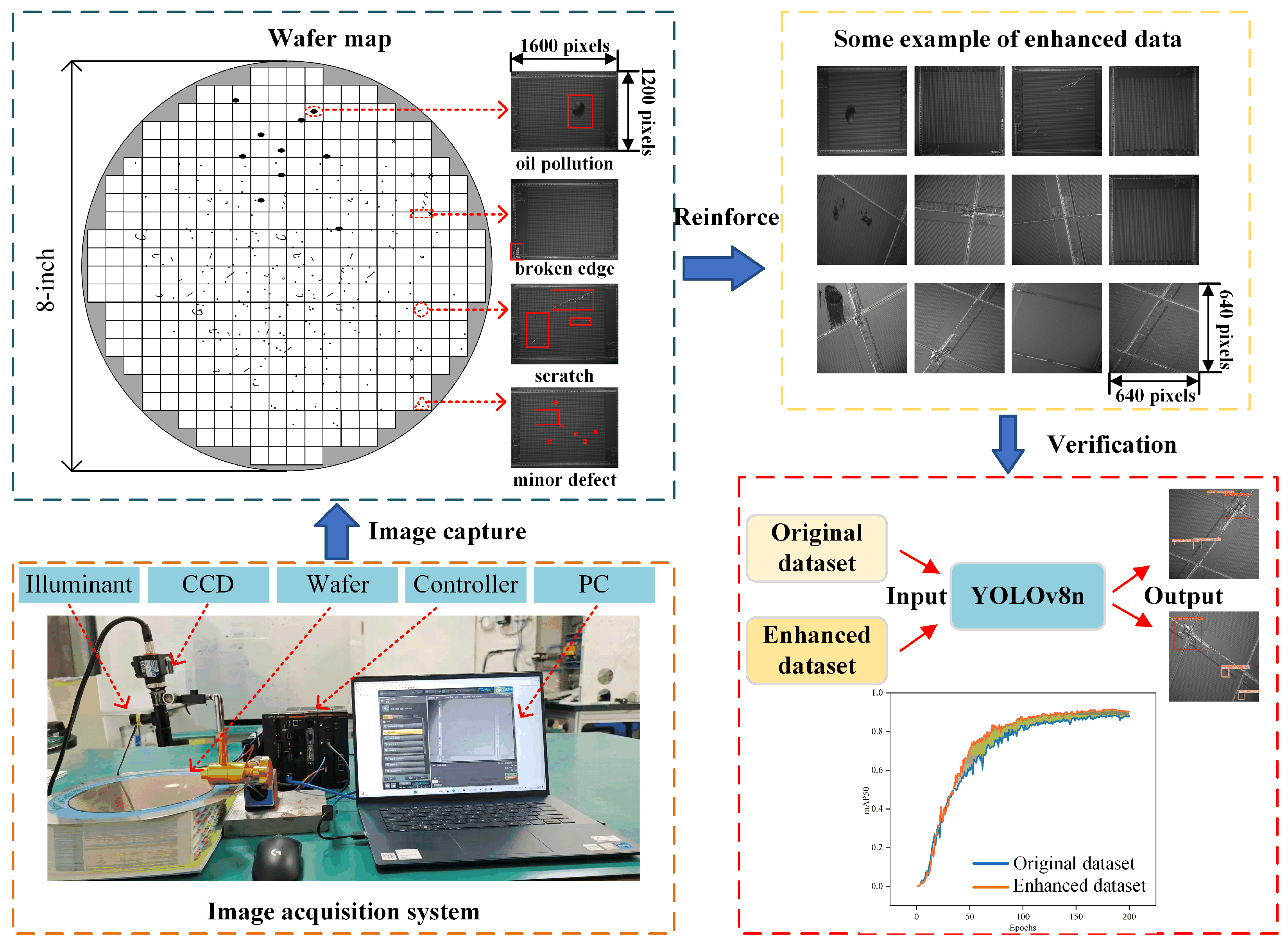
Given the scarcity of publicly accessible defective die datasets, we have curated a novel wafer surface defect dataset (WSDD) from a semiconductor company in Shanghai to assess the proposed model’s performance. The image acquisition system and capturing process are shown in Figure 6. The system is equipped with a CA-H500M industrial camera from Keyence Corporation (Osaka, Japan), which has a pixel cell size of 3.45 μ m, an 8× telecentric coaxial lens with a field of view of 0.9 mm × 1.1 mm, and a camera resolution of 0.43 μ m/px; the object distance between the camera and the wafer is set to 64 mm. The positional accuracy is 1.29 μ m when evaluated at 3 px. The final output image has a resolution of 1600 × 1200 pixels. Based on the properties of the images, we further classified the acquired 1021 defect images into the following four categories of defects.
(1)
Broken edges: Throughout the wafer fabrication process, consisting of handling, loading and unloading, or wafer dicing, the edge may be subjected to excessive impact or pressure, which in turn causes the edge to break. The ruptured area usually appears with apparent cracks or chips, showing an irregular shape, uneven edges, and a tendency to bifurcate or expand.
(2)
Scratches: Die scratches usually occur due to improper human operation during wafer handling, cleaning, cutting, and polishing. Linear cracks or grooves in straight, curved, or irregular shapes characterize scratches.
(3)
Oil pollution: Wafers in the production of engineering fixtures, vacuum suction cups, handling equipment, etc., may be affected by the existence of lubricating oil and grease residues, leakage problems, or friction in the process of operation, leading to oil dripping. These defects usually manifest as spots or round areas with blurred edges and noticeable color differences compared to the surfaces of other die parts.
(4)
Minor defects: Tiny defects on the surface of the grain are the most common. They are usually caused by dust, particulate matter, or impurities in the external environment, which adhere to the wafer surface and may lead to the development of defects on a larger scale. These present themselves as round or irregular shapes; their size ranges from a few micrometers to hundreds of micrometers, and they can even reach the nanometer level.
In this study, we refer to the construction method of the Pascal VOC dataset and adopt the LabeImg annotation software to annotate the above four types of grain defect images, corresponding to the labels “broken edge”, “scratch”, “oil pollution”, and “minor defect”, respectively. The small number of wafer surface defect datasets and the problem of category imbalance result in poor robustness and generalization. To enhance the training effect of the network model and to prevent overfitting during training, we employed data augmentation techniques such as rotation, scaling, brightness adjustment, and flipping to generate 2235 augmented images. The expanded dataset consists of a total of 3256 images, including the original real-world images and augmented images. All images were grouped by their original image source to ensure that one original image and all its augmented variants were not assigned across different subsets. Finally, the dataset was partitioned into training, validation, and testing sets with a ratio of 8:1:1.
All the experiments in this study were conducted on the Windows 11 operating system, using PyTorch 1.12.1 as the deep learning framework. The hardware configuration of the experiments included an NVIDIA GeForce RTX 3060 GPU (NVIDIA Corporation, Santa Clara, CA, USA) equipped with 6 GB of video memory, an Intel Core i7-12700H CPU (Intel Corporation, Santa Clara, CA, USA) with 32 GB of RAM. The software environment included Python 3.9 and CUDA 11.6. In addition, the input image dimensions were consistently standardized to 640 × 640 pixels. Table 1 details the fixed hyperparameters set to ensure the experiment’s fairness and reproducibility.

3.2. Ablation Experiment

To quantitatively assess the empirical validity of the network architecture optimization strategies and their consistency with theoretical derivations, YOLOv8n is utilized as the baseline model for the ablation experiments in the present study, during which the precision (P), recall (R), and mean average precision (mAP) are used as metrics to evaluate the overall performance of the model. The formulas of the related evaluation indices are as follows:
P = T P T P + F P , R = T P T P + F N
A P = 0 1 P ( R ) d R
m A P = 1 N i = 1 i A P i
where TP represents the number of instances correctly classified as positive by the model, FP indicates the number of instances incorrectly classified as positive, and FN signifies the number of instances incorrectly classified as negative. P and R are used to assess the accuracy of the positive predictions and to measure the model’s ability to detect instances of the positive categories, respectively. AP is used to reflect the model’s performance in the detection of individual categories, N denotes the total number of categories, and mAP reflects the model’s overall detection performance.
This research addresses the real-time detection of wafer surface defects in the industry domain, which requires the proposed model to have the properties of a light weight, a high frame rate, and low computational effort. Thus, we consider the effects of the parameters and FLOPs on the model’s complexity. Furthermore, the model’s real-time image processing capability is evaluated by the number of frames per second (FPS). The higher the FPS value, the faster the inference and the more frames of images are processed per unit of time. The calculation formula is
F P S = 1000 p r e + i n + N M S
where p r e represents the image preprocessing time, i n represents the inference time, and N M S represents the postprocessing per image. The experimental results are shown in Table 2.
The experimental results in Table 2 show that, firstly, replacing the C2f module with the IGC module in the YOLOv8n backbone network (model b) reduces the number of parameters and FLOPs by 0.43 M and 1.4 G, respectively, thereby lowering the model’s complexity. Utilizing the CCFF-ISC neck network alone (model c) reduces the parameters and FLOPs to 2.00 M and 5.7 G, respectively, while maintaining the mAP50 at 92.3%. Employing the DyHeadv3 module independently (model d) results in a relatively small reduction in computational load but increases the mAP50 to 92.0%. Further, combining the CCFF-ISC neck network with the IGC module (model e) improves the mAP50 by 1.1% compared to the baseline model, with additional reductions in parameters and FLOPs of 1.46 M and 2.9 G, respectively. This indicates that the improved neck network effectively reduces the computational burden while enhancing the accuracy. The combination of IGC and DyHeadv3 (model f) achieves an mAP50 of 91.8%. In contrast, the integration of the CCFF-ISC neck network with DyHeadv3 (model g) reaches an mAP50 of 93.2%, demonstrating the complementary advantages of the proposed modules. Finally, when DyHeadv3, IGC, and the CCFF-ISC neck network are jointly utilized (model h), the model achieves precision, recall, and mAP50 values of 92.7%, 90.8%, and 93.7%, respectively, outperforming all previously mentioned models. Despite a slight increase in parameters and FLOPs compared to model E (which lacks a dynamic detection head), the proposed model remains lightweight and achieves an inference speed of 140.5 frames per second. Compared with the baseline model, the improved CISC-YOLO increases the mAP50 by 2.4%, precision by 5.1%, and recall by 5.9%, while reducing the parameters by 1.09 M and FLOPs by 2.2 G. This achieves an effective balance between accuracy and computational load, while reducing missed detections and false detections of wafer defects.
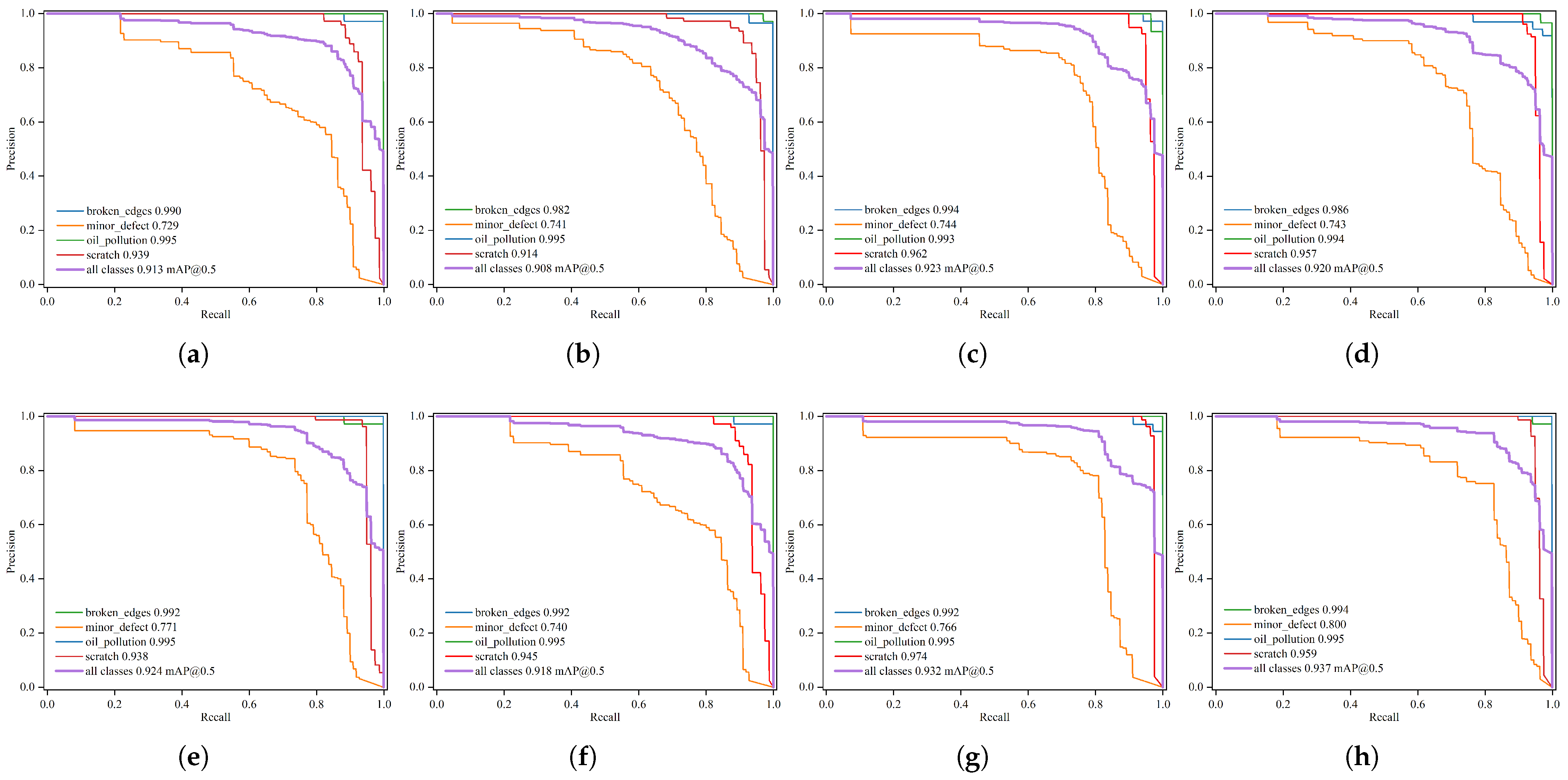
Notably, as observed from the precision–recall (P-R) curves in Figure 7, the curve corresponding to each improved model (from a to h) lies closer to the upper-right corner, indicating that the model exhibits a more favorable trade-off between precision and recall. The final model h achieves the most significant area under the curve (AUC), which implies its ability to detect more targets accurately, with fewer false positives or false negatives. Specifically, for the small defect category, the improvement in the AP50 is significant, as reflected in the enhanced performance curves for categories such as “minor defects”. The consistent overall improvement in the curves verifies that each module contributes to more effective multi-scale and small-target detection, thus confirming the effectiveness of each component in the ablation study.

3.3. Comparison Experiment

To validate the advantages of CISC-YOLO in industrial target detection, this section first designs and implements two lightweight improvement schemes to explore their impacts on the detection accuracy while achieving a light weight, according to Table 3. One of these seeks to replace the backbone network with the classical lightweight network structures that have been widely used in recent years, such as ShuffleNetV2 [29], MobileNetV3 [30], EfficientViT [31], and StarNet [32]. The second seeks to continue the IGC module design concept proposed in this study by replacing the convolutional layers in the entire network C2f structure with lightweight convolutional layers, such as HetConv [33], PConv [34], DualConv [35], and WTConv [36]. Furthermore, to more rigorously evaluate the advantages of the proposed algorithms, several representative target detection algorithms are selected for a comparative study, including Faster R-CNN [12], the RT-DETR series [37,38], SSD [20], and the commonly used YOLO series of algorithms, with the corresponding experimental results presented in Table 4. Finally, to comprehensively evaluate the generalization capabilities of the enhanced model, two typical public datasets from industrial scenarios are selected for validation in this study. The first dataset consists of 737 PCB [39] images containing six classes of small-scale defects, and the second is NEU-DET [40], a steel surface defect dataset with six classes of complex backgrounds. The aim is to verify the adaptability and robustness of the improved model under different scenarios and tasks, with the detailed experimental results presented in Table 5.
The results outlined in Table 3 demonstrate that, despite the sub-optimal mAP50 obtained when the MobileNetV3 backbone is adopted, with a value of 92.6%, its 4.31 M parameter quantity and 8.7 MB model volume are 124% and 117% higher than those of CISC-YOLO, respectively, suggesting that, although MobileNetV3 is a lightweight backbone network, the additional overhead associated with its fusion with subsequent features significantly increases the overall model complexity. The Transformer-based EfficientViT architecture achieves a 91.7% mAP50, but the secondary computational complexity due to its self-attention mechanism causes the FLOPs to surge to 25.1 G, which severely reduces the feasibility of real-time deployment. In addition, although the lightweight performance is improved when the baseline model is modified by adopting lightweight backbones (ShuffleNetv2, StarNet) or mainstream lightweight convolutions, its mAP50 decreases in all cases, failing to achieve a good balance between detection accuracy and lightweight performance. In contrast, the proposed algorithm in this study achieves optimal detection accuracy, while its 1.92 M parameters and 6.0 G FLOPs demonstrate the superiority of the lightweight design under limited computational resources.
Table 4 indicates that traditional detection models such as Faster R-CNN, RT-DETR-L, and SSD have relatively low precision and enormous computational costs, exposing their shortcomings in small target detection and the inefficient use of computational resources. Although RT-DETR-MobileNetV4 and MDD-DETR perform well in terms of the mAP50 and FPS, their computational complexity and parameter counts are still relatively large. In the comparison of the YOLO series, YOLOv5n achieves extreme lightweightness, with 1.82 M parameters and an 89% mAP50. However, there is a 4.7% precision gap compared with CISC-YOLO, making it prone to missing and false detections in multi-scale target detection. The mAP50s of YOLOv6n and YOLOv7-tiny are slightly better than that of YOLOv8n; however, their FLOPs and parameter counts increase by 98.3%/106.7% and 120.8%/213.5%, respectively, compared with CISC-YOLO, highlighting the significant computational cost accompanying performance improvement. In contrast, CISC-YOLO achieves a 93.7% mAP50 with 1.92 M parameters, outperforming other mainstream algorithms in balancing detection precision and computational efficiency, further demonstrating its effectiveness.
Figure 8 illustrates the growth trends of the mAP50 metric and the convergence rates of the validation loss for all models listed in Table 4 during the target detection task. Figure 8a shows that CISC-YOLO achieves an mAP50 of over 80% within 60 training epochs, outperforming other detection models; its curve exhibits a pattern of rapid increase and smooth convergence, which indicates that the model possesses excellent feature extraction capabilities in the early stages of training and confirms that the proposed dynamic feature fusion strategy can effectively accelerate model learning. The curves of Faster R-CNN, RT-DETR-L, and SSD exhibit slow growth with large fluctuations, necessitating 140–160 training epochs to achieve the same level of accuracy, which highlights their unstable training nature. In addition, the loss curves of the baseline models YOLOv8n and CISC-YOLO in Figure 8b are smoother and they perform better compared with other models; notably, CISC-YOLO has the fastest loss reduction rate and the lowest final loss value, which means that the model can significantly shorten the training cycle and reduce the training costs. In summary, this further confirms that CISC-YOLO is superior to the aforementioned mainstream models in terms of accuracy, convergence speed, and lightweight performance, making it more suitable for real-time deployment in industrial inspection scenarios.
As shown in Table 5, in the scenario of PCB industrial defect detection, the CISC-YOLO algorithm outperforms all comparative models, with an mAP50 metric of 93.6%, which is a 2.0% improvement compared to the sub-optimal model MDD-DETR. Additionally, its precision and recall rates reach 95.5% and 89.9%, respectively, both exceeding those of other algorithms. This indicates that the improved network effectively enhances the ability to characterize the features of tiny solder joint defects. Furthermore, on the NEU-DET dataset of complex surface defects, CISC-YOLO achieves higher mAP50, precision, and recall values than all other comparative models, thereby confirming that CISC-YOLO possesses strong generalization capabilities.

3.4. Visualization of Results

To validate the performance, this study selects raw images containing multiple types of wafer defects from the test set for verification, and these images cover defects of different scales, shapes, and locations. Meanwhile, the proposed method is compared with the mainstream algorithms listed in Table 4. The experimental results are presented in Figure 9.
The visualization results show that, in the detection of oil-type defects on wafers, Faster R-CNN, RT-DETR-L, RT-DETR-MobileNetV4, SSD, and YOLOv5n can achieve relatively high accuracy; however, they have obvious limitations in handling small-scale targets, resulting in multiple missed detections. In addition, when identifying two types of dense targets, these models have insufficient confidence in distinguishing between targets and complex backgrounds, which in turn leads to overlapping prediction boxes. MDD-DETR, YOLOv6n, YOLOv7-tiny, and YOLOv8n have improved issues such as missed detections and redundant bounding boxes; however, for minimal defects that are obscured by background noise or fused with the background, there are still a small number of missed detections, and the models struggle to achieve accurate differentiation. In contrast, the CISC-YOLO model proposed in this study achieves accuracy of over 90% in various defect detection tasks. In terms of tiny defect detection, it effectively solves problems such as missed detections, false detections, and overlapping prediction boxes, with comprehensive performance superior to that of other mainstream models.

4. Conclusions

This article proposes a lightweight inspection model based on YOLOv8, named CISC-YOLO, to detect tiny defects on the surfaces of semiconductor wafers. Firstly, the IGC module reconstructed with GhostConv is integrated into the backbone network, significantly reducing the computational load caused by redundant features. Secondly, the CCFF-ISC neck network enhances the expressive capability for cross-scale features, enabling more efficient information fusion. Finally, the dynamic detection head, DyHeadv3, through the synergistic effects of scale-aware, space-aware, and task-aware attention mechanisms, remarkably improves the model’s positioning accuracy for dense micro-defects. Ablation experiments and multiple groups of comparative experiments verify that the proposed model exhibits superior robustness in complex backgrounds with small targets. Meanwhile, CISC-YOLO also demonstrates favorable generalization performance on the PCB and NEU-DET datasets. Future research will focus on more efficient operator fusion strategies to enhance the model’s multi-scale detection capabilities; additionally, it will explore model distillation techniques to compress the model size further, enabling it to adapt to low-power embedded devices and provide a more universal detection solution for intelligent semiconductor manufacturing.

Author Contributions

Methodology, Y.C. and B.Z.; data acquisition, B.Z. and X.G.; writing—original draft, Y.C., X.G., B.Z. and L.Y.; funding acquisition: Y.C. and L.Y. All authors have read and agreed to the published version of the manuscript.

Funding

This work was supported in part by the National Natural Science Foundation of China under Grant 62172281 and Grant 51605294.

Data Availability Statement

The original contributions presented in this study are included in the article. Further inquiries can be directed to the corresponding author.

Conflicts of Interest

The authors declare no conflicts of interest.

References

  1. Jin, Q.; Jiang, Y.; Lu, X.; Liu, Y.; Chen, Y.; Gao, D.; Sun, Q.; Zhuo, C. SEM-CLIP: Precise few-shot learning for nanoscale defect detection in scanning electron microscope image. In Proceedings of the ICCAD ’24: 43rd IEEE/ACM International Conference on Computer-Aided Design, New York, NY, USA, 27–31 October 2024; pp. 1–8. [Google Scholar]
  2. Wang, J.; Hu, H.; Pan, C.; Zhou, Y.; Li, L. Scheduling dual-arm cluster tools with multiple wafer types and residency time constraints. IEEE/CAA J. Autom. Sin. 2020, 7, 776–789. [Google Scholar] [CrossRef]
  3. Kim, T.; Behdinan, K. Advances in machine learning and deep learning applications towards wafer map defect recognition and classification: A review. J. Intell. Manuf. 2023, 34, 3215–3247. [Google Scholar] [CrossRef]
  4. Wang, Z.; Su, K.; Zhang, J.; Jia, H.; Ye, Q.; Xie, X.; Lu, Z. Multi-agent automated machine learning. In Proceedings of the 2023 IEEE/CVF Conference on Computer Vision and Pattern Recognition (CVPR), Vancouver, BC, Canada, 17–24 June 2023; pp. 11960–11969. [Google Scholar]
  5. Zhao, Y.; Ball, R.; Mosesian, J.; de Palma, J.F.; Lehman, B. Graph-based semi-supervised learning for fault detection and classification in solar photovoltaic arrays. IEEE Trans. Power Electron. 2014, 30, 2848–2858. [Google Scholar] [CrossRef]
  6. Yuan, T.; Kuo, W.; Bae, S.J. Detection of spatial defect patterns generated in semiconductor fabrication processes. IEEE Trans. Semicond. Manuf. 2011, 24, 392–403. [Google Scholar] [CrossRef]
  7. Gómez-Sirvent, J.L.; de la Rosa, F.L.; Sánchez-Reolid, R.; Fernández-Caballero, A.; Morales, R. Optimal feature selection for defect classification in semiconductor wafers. IEEE Trans. Semicond. Manuf. 2022, 35, 324–331. [Google Scholar] [CrossRef]
  8. Xie, L.; Huang, R.; Gu, N.; Cao, Z. A novel defect detection and identification method in optical inspection. Neural Comput. Appl. 2014, 24, 1953–1962. [Google Scholar] [CrossRef]
  9. Pouyanfar, S.; Sadiq, S.; Yan, Y.; Tian, H.; Tao, Y.; Reyes, M.P.; Shyu, M.L.; Chen, S.C.; Iyengar, S.S. A survey on deep learning: Algorithms, techniques, and applications. ACM Comput. Surv. 2018, 51, 1–36. [Google Scholar] [CrossRef]
  10. Wang, X.; Wang, S.; Liang, X.; Zhao, D.; Huang, J.; Xu, X.; Dai, B.; Miao, Q. Deep reinforcement learning: A survey. IEEE Trans. Neural Netw. Learn. Syst. 2022, 35, 5064–5078. [Google Scholar] [CrossRef]
  11. Ren, S.; He, K.; Girshick, R.; Sun, J. Faster R-CNN: Towards real-time object detection with region proposal networks. IEEE Trans. Pattern Anal. Mach. Intell. 2016, 39, 1–36. [Google Scholar] [CrossRef]
  12. Dai, J.; Li, Y.; He, K.; Sun, J. R-FCN: Object detection via region-based fully convolutional networks. In Proceedings of the Advances in Neural Information Processing Systems 29: Annual Conference on Neural Information Processing Systems 2016, Barcelona, Spain, 5–10 December 2016; pp. 1–9. [Google Scholar]
  13. He, K.; Gkioxari, G.; Dollár, P.; Girshick, R. Mask R-CNN. In Proceedings of the 2017 IEEE International Conference on Computer Vision (ICCV), Venice, Italy, 22–29 October 2017; pp. 2980–2988. [Google Scholar]
  14. Zhuang, J.; Mao, G.; Wang, Y.; Chen, X.; Wang, Y.; Wei, Z. Classification of wafer backside images via FasterRCNN-based neural network. In Proceedings of the 2022 China Semiconductor Technology International Conference (CSTIC), Shanghai, China, 20–21 June 2022; pp. 1–4. [Google Scholar]
  15. Wu, H.; Gao, W.; Xu, X. Solder joint recognition using mask R-CNN method. IEEE Trans. Compon. Packag. Manuf. Technol. 2019, 10, 525–530. [Google Scholar] [CrossRef]
  16. Redmon, J.; Divvala, S.; Girshick, R.; Farhadi, A. You only look once: Unified, real-time object detection. In Proceedings of the 2016 IEEE Conference on Computer Vision and Pattern Recognition (CVPR), Las Vegas, NV, USA, 27–30 June 2016; pp. 779–788. [Google Scholar]
  17. Li, C.; Li, L.; Jiang, H.; Weng, K.; Geng, Y.; Li, L.; Ke, Z.; Li, Q.; Cheng, M.; Nie, W.; et al. YOLOv6: A single-stage object detection framework for industrial applications. arXiv 2020, arXiv:2209.02976. [Google Scholar]
  18. Shinde, P.P.; Pai, P.P.; Adiga, S.P. Wafer defect localization and classification using deep learning techniques. IEEE Access 2022, 10, 39969–39974. [Google Scholar] [CrossRef]
  19. Tao, Q.; Chen, Y.; Chen, H. A detection approach for wafer detect in industrial manufacturing based on YOLOv8. In Proceedings of the 13th CAA Symposium on Fault Detection, Supervision, and Safety for Technical Processes (CAA SAFEPROCESS 2023), Yibin, China, 22–24 September 2023; pp. 1–6. [Google Scholar]
  20. Liu, W.; Anguelov, D.; Erhan, D.; Szegedy, C.; Reed, S.; Fu, C.Y.; Berg, A.C. SSD: Single shot multibox detector. In Proceedings of the 14th European Conference on Computer Vision—ECCV 2016, Amsterdam, The Netherlands, 11–14 October 2016; pp. 21–37. [Google Scholar]
  21. Wang, S.; Wang, H.; Yang, F.; Liu, F.; Zeng, L. Attention-based deep learning for chip-surface-defect detection. Int. J. Adv. Manuf. Technol. 2022, 121, 1957–1971. [Google Scholar] [CrossRef]
  22. Li, D.; Lu, Y.; Gao, Q.; Li, X.; Yu, X.; Song, Y. LiteYOLO-ID: A lightweight object detection network for insulator defect detection. IEEE Trans. Instrum. Meas. 2024, 73, 1–12. [Google Scholar] [CrossRef]
  23. Zhou, W.; Li, C.; Ye, Z.; He, Q.; Ming, Z.; Chen, J.; Wan, F.; Xiao, Z. An efficient tiny defect detection method for PCB with improved YOLO through a compression training strategy. IEEE Trans. Instrum. Meas. 2024, 73, 1–14. [Google Scholar] [CrossRef]
  24. Wang, H.; Liu, C.; Cai, Y.; Chen, L.; Li, Y. YOLOv8-QSD: An improved small object detection algorithm for autonomous vehicles based on YOLOv8. IEEE Trans. Instrum. Meas. 2024, 73, 1–16. [Google Scholar] [CrossRef]
  25. Sandler, M.; Howard, A.; Zhu, M.; Zhmoginov, A.; Chen, L.C. Mobilenetv2: Inverted residuals and linear bottlenecks. In Proceedings of the 2018 IEEE/CVF Conference on Computer Vision and Pattern Recognition (CVPR), Salt Lake City, UT, USA, 18–22 June 2018; pp. 4510–4520. [Google Scholar]
  26. Si, Y.; Xu, H.; Zhu, X.; Zhang, W.; Dong, Y.; Chen, Y.; Li, H. SCSA: Exploring the synergistic effects between spatial and channel attention. Neurocomputing 2025, 634, 129866. [Google Scholar] [CrossRef]
  27. Dai, X.; Chen, Y.; Xiao, B.; Chen, D.; Liu, M.; Yuan, L.; Zhang, L. Dynamic head: Unifying object detection heads with attentions. In Proceedings of the IEEE/CVF Conference on Computer Vision and Pattern Recognition (CVPR), Virtual, 19–25 June 2021; pp. 7373–7382. [Google Scholar]
  28. Wang, W.; Dai, J.; Chen, Z.; Huang, Z.; Li, Z.; Zhu, X.; Hu, X.; Lu, T.; Lu, L.; Li, H.; et al. Internimage: Exploring large-scale vision foundation models with deformable convolutions. In Proceedings of the IEEE/CVF Conference on Computer Vision and Pattern Recognition (CVPR), Vancouver, BC, Canada, 17–24 June 2023; pp. 14408–14419. [Google Scholar]
  29. Ma, N.; Zhang, X.; Zheng, H.T.; Sun, J. Shufflenet v2: Practical guidelines for efficient cnn architecture design. In Proceedings of the 15th European Conference on Computer Vision—ECCV 2018, Munich, Germany, 8–14 September 2018; pp. 116–131. [Google Scholar]
  30. Howard, A.; Sandler, M.; Chu, G.; Chen, L.C.; Chen, B.; Tan, M.; Wang, W.; Zhu, Y.; Pang, R.; Vasudevan, V.; et al. Searching for mobilenetv3. In Proceedings of the IEEE/CVF International Conference on Computer Vision (ICCV), Seoul, Republic of Korea, 27 October–2 November 2019; pp. 1314–1324. [Google Scholar]
  31. Liu, X.; Peng, H.; Zheng, N.; Yang, Y.; Hu, H.; Yuan, Y. Efficientvit: Memory efficient vision transformer with cascaded group attention. In Proceedings of the IEEE/CVF Conference on Computer Vision and Pattern Recognition (CVPR), Vancouver, BC, USA, 18–22 June 2023; pp. 14420–14430. [Google Scholar]
  32. Ma, X.; Dai, X.; Bai, Y.; Wang, Y.; Fu, Y. Rewrite the stars. In Proceedings of the IEEE/CVF Computer Vision and Pattern Recognition Conference (CVPR), Seattle, WA, USA, 17–21 June 2024; pp. 5694–5703. [Google Scholar]
  33. Singh, P.; Verma, V.K.; Rai, P.; Namboodiri, V.P. HetConv: Heterogeneous kernel-based convolutions for deep CNNs. In Proceedings of the IEEE/CVF Computer Vision and Pattern Recognition Conference (CVPR), Long Beach, CA, USA, 15–20 June 2019; pp. 4835–4844. [Google Scholar]
  34. Park, S.; Yeo, Y.J.; Shin, Y.G. PConv: Simple yet effective convolutional layer for generative adversarial network. Neural Comput. Appl. 2022, 34, 7113–7124. [Google Scholar] [CrossRef]
  35. Zhong, J.; Chen, J.; Mian, A. DualConv: Dual convolutional kernels for lightweight deep neural networks. IEEE Trans. Neural Netw. Learn. Syst. 2022, 34, 9528–9535. [Google Scholar] [CrossRef] [PubMed]
  36. Finder, S.E.; Amoyal, R.; Treister, E.; Freifeld, O. Wavelet convolutions for large receptive fields. In Proceedings of the European Conference on Computer Vision (ECCV), Milan, Italy, 29 September–4 October 2024; pp. 363–380. [Google Scholar]
  37. Zhao, Y.; Lv, W.; Xu, S.; Wei, J.; Wang, G.; Dang, Q.; Liu, Y.; Chen, J. Detrs beat YOLOs on real-time object detection. In Proceedings of the IEEE/CVF Computer Vision and Pattern Recognition Conference (CVPR), Seattle, WA, USA, 17–21 June 2024; pp. 16965–16974. [Google Scholar]
  38. Peng, J.; Fan, W.; Lan, S.; Wang, D. MDD-DETR: Lightweight detection algorithm for printed circuit board minor defects. Electronics 2024, 13, 4453. [Google Scholar] [CrossRef]
  39. Yao, L.; Zhao, B.; Wang, X.; Mei, S.; Chi, Y. A detection algorithm for surface defects of printed circuit board based on improved YOLOv8. IEEE Access 2024, 12, 170227–170242. [Google Scholar] [CrossRef]
  40. Liu, H.; Hu, R.; Dong, H.; Liu, Z. SFC-YOLOv8: Enhanced strip steel surface defect detection using spatial-frequency domain optimized YOLOv8. IEEE Trans. Instrum. Meas. 2025, 74, 1–11. [Google Scholar] [CrossRef]
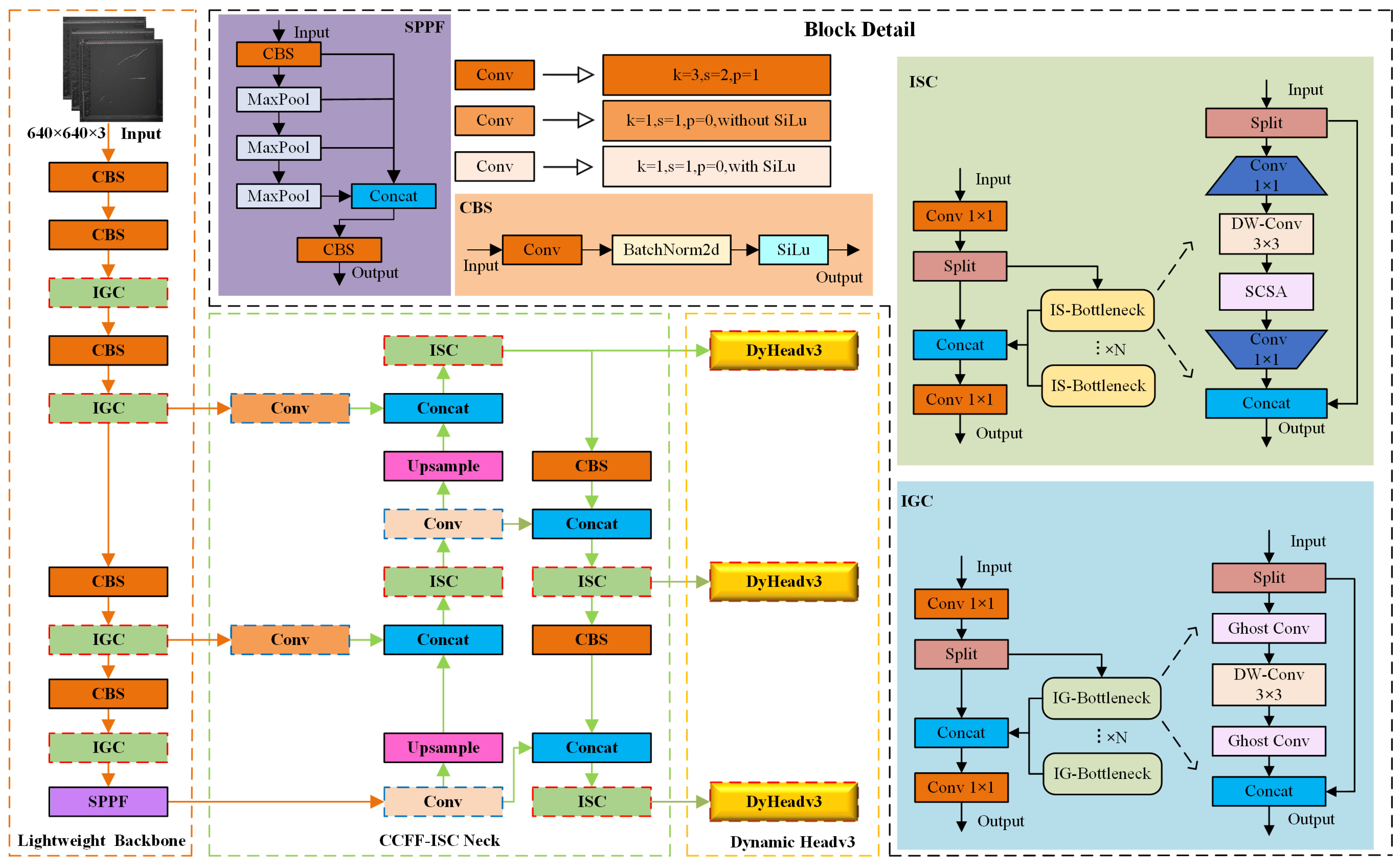
Figure 1. Wafer defect detection model of CISC-YOLO. The red dotted boxes indicate the modular improvements in the backbone mesh, the necking mesh, and the detection head, respectively. The blue dashed box indicates the convolution with a kernel of 1 introduced in the necking mesh. Orange arrows: Feature transmission from the backbone network to the neck network. Green arrows: Transmission of multi-scale feature fusion results from the neck network to the head network. Black solid arrows: Detailed computational flow of specific modules within YOLOv8. Black dashed arrows: Bottleneck sections within the improved modules (ISC/IGC), involving enhancements to internal residual or attention connections.
Electronics 14 03960 g001
Figure 2. Schematic diagram of the operation of GhostConv. (a) Conventional convolutional module. (b) Ghost convolutional module.
Electronics 14 03960 g002
Figure 3. Architecture of the CCFF.
Electronics 14 03960 g003
Figure 4. SCSA attention mechanism.
Electronics 14 03960 g004
Figure 5. Network structure of DyHeadv3.
Electronics 14 03960 g005
Figure 6. Image acquisition system. We enhanced the original image and validated it using a baseline algorithm, which showed that the mAP50 obtained from the enhanced data was significantly better than that of the original image.
Electronics 14 03960 g006
Figure 7. Precision–recall curves. (a) YOLOv8n. (b) YOLOv8n+IGC. (c) YOLOv8n+CCFF_ISC_neck. (d) YOLOv8n+DyHeadv3. (e) YOLOv8n+IGC+CCFF_ISC_neck. (f) YOLOv8n+IGC+DyHeadv3. (g) YOLOv8n+CCFF_ISC_neck+DyHeadv3. (h) YOLOv8n+IGC+CCFF_ISC_neck+DyHeadv3.
Electronics 14 03960 g007
Figure 8. Curve diagrams of comparison results of mainstream algorithms. (a) mAP50. (b) Validation loss.
Electronics 14 03960 g008
Figure 9. Visualization results of mainstream algorithms.
Electronics 14 03960 g009
Table 1. Training hyperparameter configuration.
ParameterValue
Epochs200
Batch size8
Initial learning rate0.001
OptimizerSGD
Weight decay0.005
Momentum0.937
Table 2. Comparison of ablation experiments.
ModelIGCCCFF_ISC NeckDyHeadv3P (%)R (%)mAP50 (%)Params (M)FLOPs (G)FPS
a 87.684.991.33.018.2121.3
b 82.585.690.82.586.8133.4
c 88.386.592.32.005.7141.2
d 89.287.392.02.987.9126.5
e 92.089.592.41.555.3152.4
f 91.589.391.82.536.6137.8
g 91.889.993.21.976.2138.1
h92.790.893.71.926.0140.5
Table 3. Comparative experiment on lightweight improvement.
ModelParams (M)Size (MB)FLOPs (G)mAP50 (%)
YOLOv8n3.016.08.291.3
YOLOv8n-ShuffleNetv22.795.77.590.7
YOLOv8n-EfficientViT2.495.225.191.7
YOLOv8n-MobileNetv34.318.78.092.6
YOLOv8n-StarNet2.194.46.389.8
YOLOv8n-C2f_HetConv2.384.86.687.9
YOLOv8n-C2f_PConv2.314.66.483.6
YOLOv8n-C2f_DualConv2.715.47.490.8
YOLOv8n-C2f_WTConv2.645.37.288.6
Ours1.924.06.093.7
Table 4. Comparative results of mainstream algorithms for target detection.
ModelBackboneP (%)R (%)mAP50 (%)Params (M)FLOPs (G)FPS
Faster R-CNNResNet-5084.579.484.641.31232.121.5
RT-DETR-LHGNetv285.876.483.631.82109.589.6
MDD-DETRMDDNet87.489.291.513.3636.1118.9
RT-DETR-MobileNetV4MobileNetV486.888.490.811.4326.8105.3
SSDVGG1677.076.183.426.8762.554.2
YOLOv5nCSPDarkNet83.386.489.01.824.4143.8
YOLOv6nEfficientRep91.087.091.84.2411.9153.6
YOLOv7-tinyE-ELAN88.688.292.06.0212.4108.4
YOLOv8nCSPDarkNet87.684.991.33.018.2121.3
CISC-YOLOImprove CSPDarkNet92.790.893.71.926.0140.5
Table 5. The results of comparative experiments on the PCB and NEU-DET datasets.
DatasetModelP (%)R (%)mAP50 (%)
PCBFaster R-CNN85.179.385.2
MDD-DETR92.386.291.6
RT-DETR-MobileNetV492.185.490.3
YOLOv5n89.981.287.3
YOLOv6n75.866.672.0
YOLOv7-tiny94.686.791.5
YOLOv8n94.485.691.2
CISC-YOLO95.589.993.6
NEU-DETFaster R-CNN69.563.268.2
MDD-DETR70.267.572.5
RT-DETR-MobileNetV470.867.271.9
YOLOv5n64.767.870.4
YOLOv6n68.965.071.7
YOLOv7-tiny68.465.371.2
YOLOv8n70.665.472.9
CISC-YOLO76.669.273.8
Disclaimer/Publisher’s Note: The statements, opinions and data contained in all publications are solely those of the individual author(s) and contributor(s) and not of MDPI and/or the editor(s). MDPI and/or the editor(s) disclaim responsibility for any injury to people or property resulting from any ideas, methods, instructions or products referred to in the content.