1. Introduction
Analog switches are used in a wide range of applications, including Micro-Electro-Mechanical Systems (MEMSs) [
1], Battery Management Systems (BMSs) [
2], and Ultrasound Imaging Systems (UISs) [
3]. As power or signal switches, they play a critical role in connecting electronic interfaces to their respective loads. To support diverse system requirements, analog switches must be capable of carrying low- and high-voltage signals in either polarity.
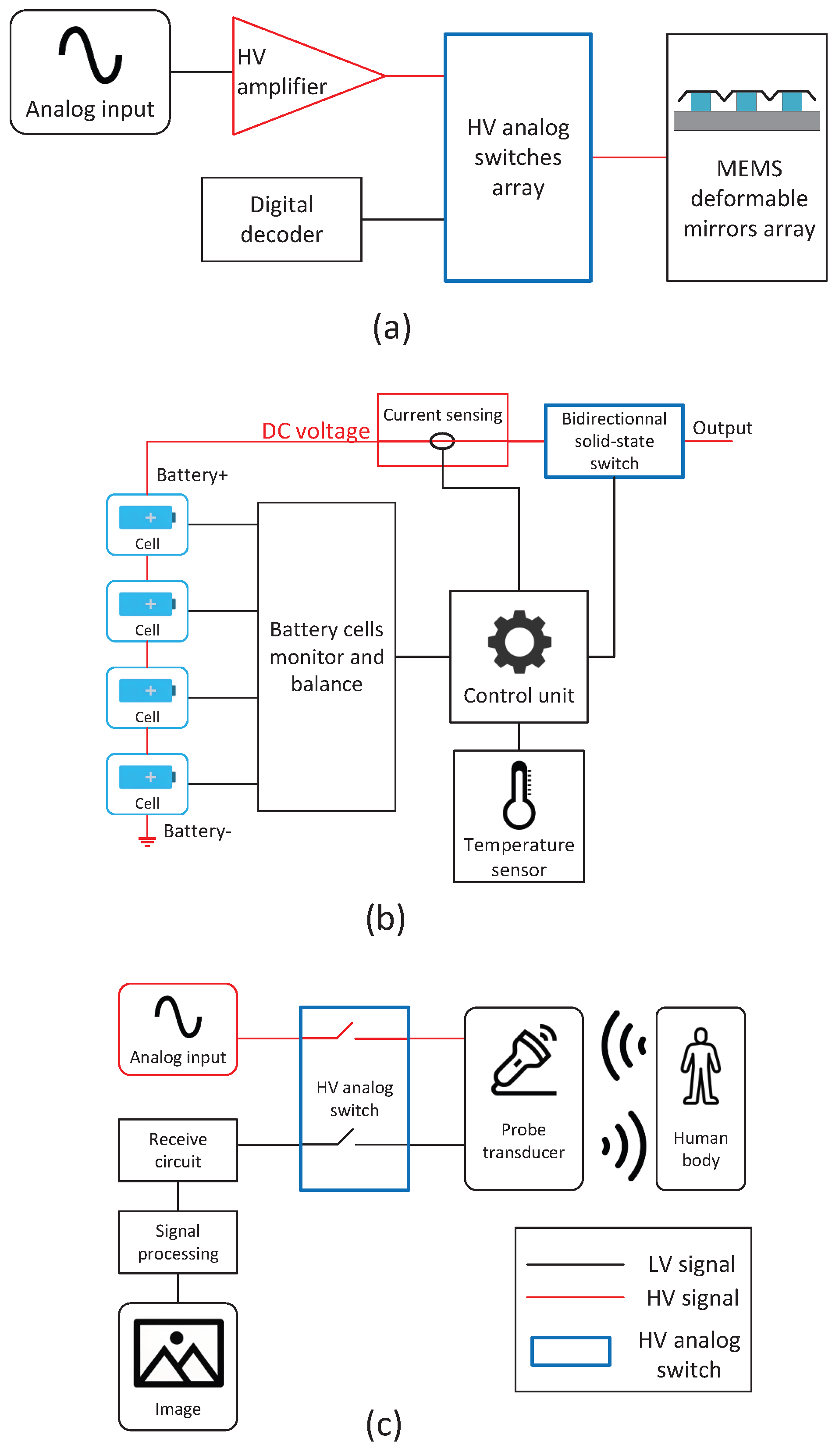
Figure 1 provides an overview of typical analog switch applications. In MEMSs, specifically in deformable mirror arrays, shown in
Figure 1a, an array of analog switches is controlled by a low-voltage decoder and delivers high-voltage analog signals to the mirrors. In BMSs, as shown in
Figure 1b, analog switches are placed between the battery and the load to control bidirectional current flow, allowing the same path for both charging and discharging currents. Unlike many other analog switch applications, BMSs operate with continuous DC voltage, whereas others typically involve varying AC signals. The most common use of analog switches is in UISs, where they transmit high voltage pulses to piezoelectric transducers, which convert electrical signals into ultrasound waves [
4]. The reflected ultrasound is then received to form an image. Since these systems require high-voltage operation, often several hundreds of volts, analog switches must withstand low-voltage receiver signals and high-voltage transmission pulses, as shown in
Figure 1c [
5].
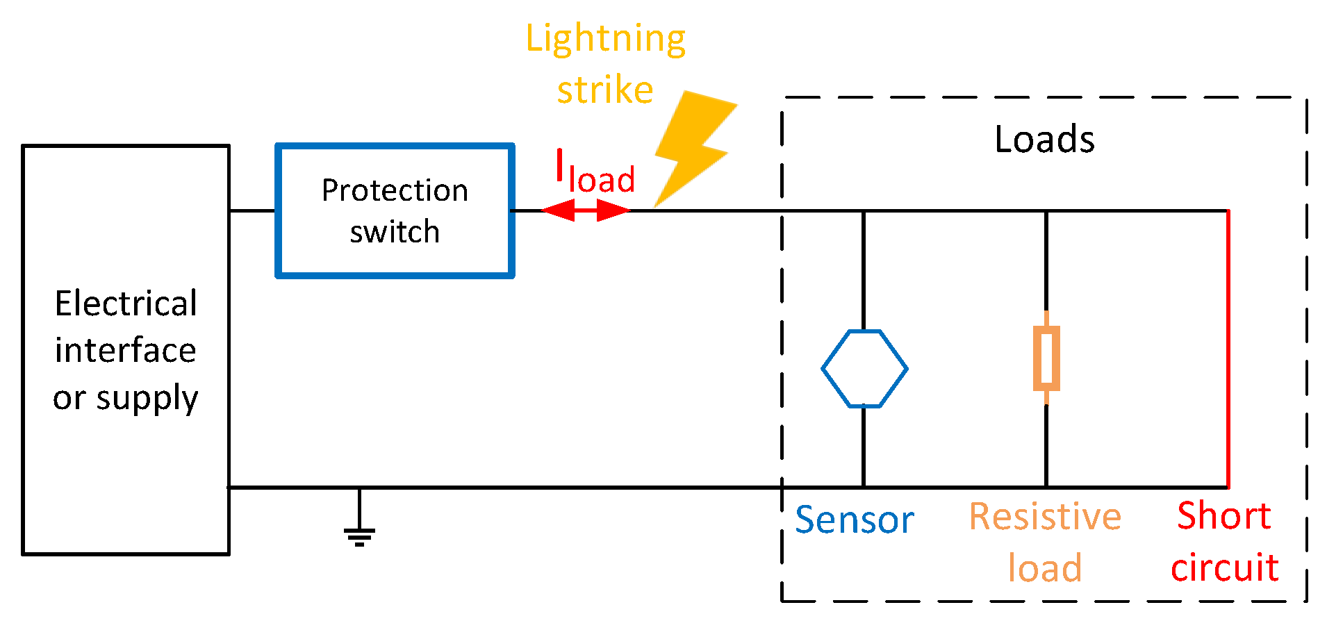
Systems featuring analog switches are often used in harsh industrial environments. For example, a BMS used in an outdoor battery application may be exposed to high humidity levels and even lightning strikes. In such conditions, electronic interfaces can suffer irreversible damage caused by single or recurrent faults on the load side, which may endanger the entire system’s operation. To mitigate the impact of such faults, analog switches in industrial systems must incorporate a protection module, which is known as an analog protection switch, as illustrated in
Figure 2. This module provides the necessary isolation to preserve interface integrity during load failures, overvoltage surges, and events that can arise from anomalies such as lightning strikes. In this work, we propose a switch architecture that brings together the most suitable circuit techniques from the literature to form a universal solution concept capable of supporting various types of loads, including resistive loads, sensors, or even short circuits in failure scenarios. Typically, a protection switch connects the load to an interface or a supply that must remain protected from a potentially damaging fault on the load side.
In modular systems such as programmable logic controllers, ports may carry either signal or power. Since the voltage and current levels present at these ports are not always known in advance, a universal analog protection switch that can carry both high current and AC voltage is essential to ensure adequate protection. Using a universal solution also enhances the reusability of the interface and reduces overall design costs. However, most of the commercial and academic solutions available are unidirectional [
6] and are powered through one of the switch terminals [
6,
7]. This approach is only viable when transferring DC signals because, in the case of an AC signal, the switch terminal cannot provide the necessary DC power for the switch and carry the AC output simultaneously. In addition, powering from the signal path can compromise signal integrity, making it unsuitable for accurate signal transmission. Existing solutions that support true analog switching are typically designed for low-current applications only and lack overcurrent protection [
5]. In contrast, available power switches cannot handle AC signals, while available signal switches are not suitable for power transfer, which will be further discussed in the upcoming section. To address these shortcomings, we propose a set of design guidelines for a universal protection switch that supports analog operation. This device will be referred to as a “protection switch” throughout the rest of this document.
To reduce system weight, cost, and power consumption, the protection switch should be fully integrated into a single package. Furthermore, monolithic integration on a single die is strongly desired to ensure compatibility with embedded systems, making standard high-voltage CMOS processes suitable. For maximum modularity, the switch must support the transmission of signals, as well as both DC and AC power. In addition, as the circuit may be used in harsh environments, it should be capable of withstanding electrical transients, such as those induced by lightning strikes, when used in conjunction with overvoltage protection devices (e.g., TVS diodes, MOV surge arresters, and varistors). Such external protections play an important role in absorbing surge energy and relaxing stress on the integrated switch [
8]. However, their co-design and detailed analysis are beyond the scope of this review paper and will be considered in future work. The switch must also include overcurrent regulation and thermal shutdown features to prevent damage.
This paper presents a design guide for synthesizing a universal, fully integrated protection switch capable of handling both DC and AC signals. The proposed architecture combines bidirectional operation, high voltage capability, and robust overcurrent protection. To the best of our knowledge, no existing commercial or academic solution has yet integrated all of these features together on a single die, underscoring the value of such a design framework. Such integration is expected to minimize system footprint, facilitate seamless incorporation into various applications, and reduce power consumption. To support this design guide, a comprehensive literature review is provided, examining solutions for each of the switch’s core components. Finally, this article is positioned as a review and design guide: we (i) establish a framework of building blocks, (ii) propose a universal architecture by selecting techniques best aligned with a proper high-voltage fabrication process, and (iii) illustrate system-level operation through behavioral simulations. Transistor-level SPICE results, silicon implementation, or measured data are outside the scope of this paper.
The remainder of this paper is organized as follows.
Section 2 examines existing commercial and academic protection switch solutions, highlighting their respective strengths and limitations.
Section 3 reviews implementation techniques for the primary high-level building blocks of the protection switch system.
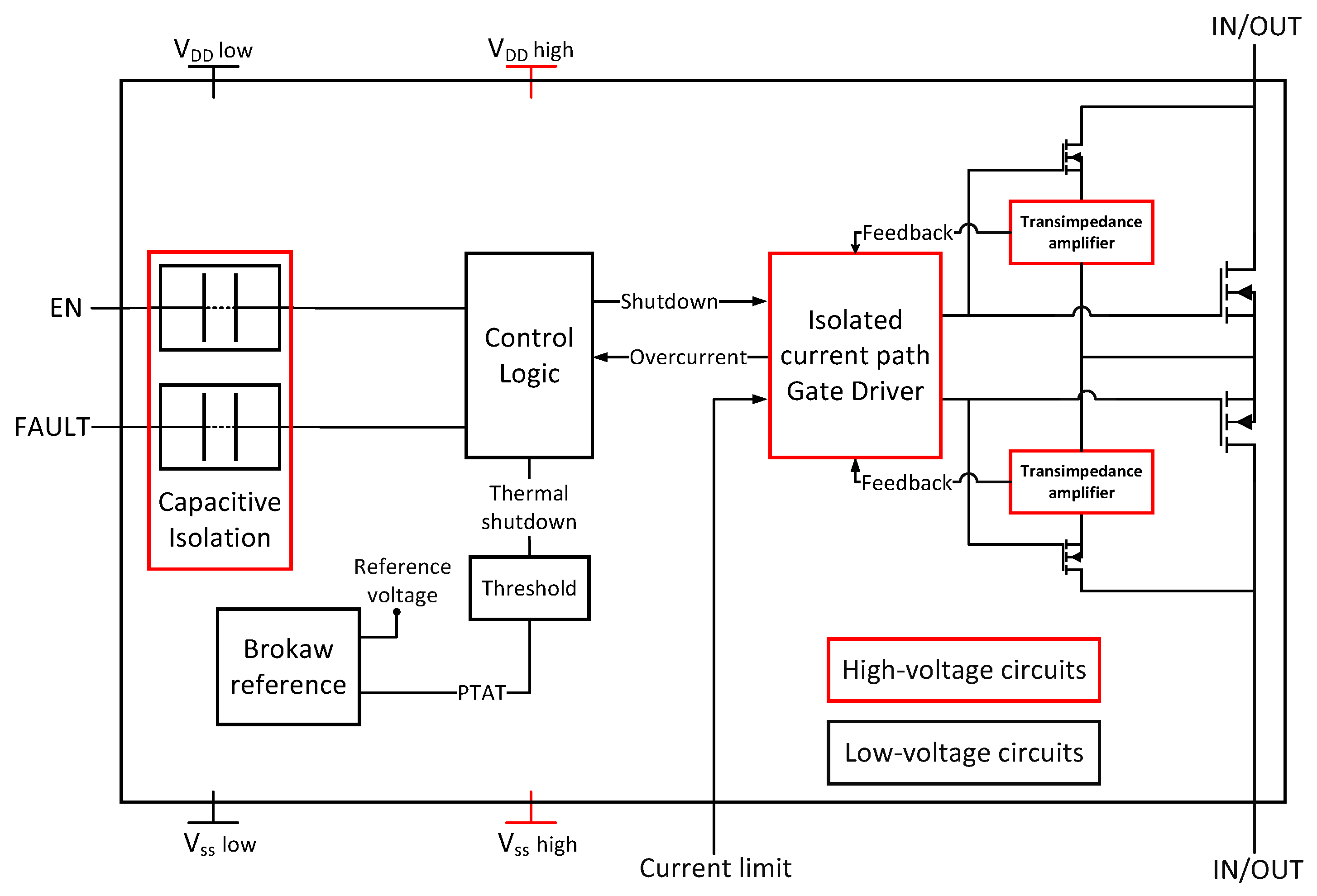
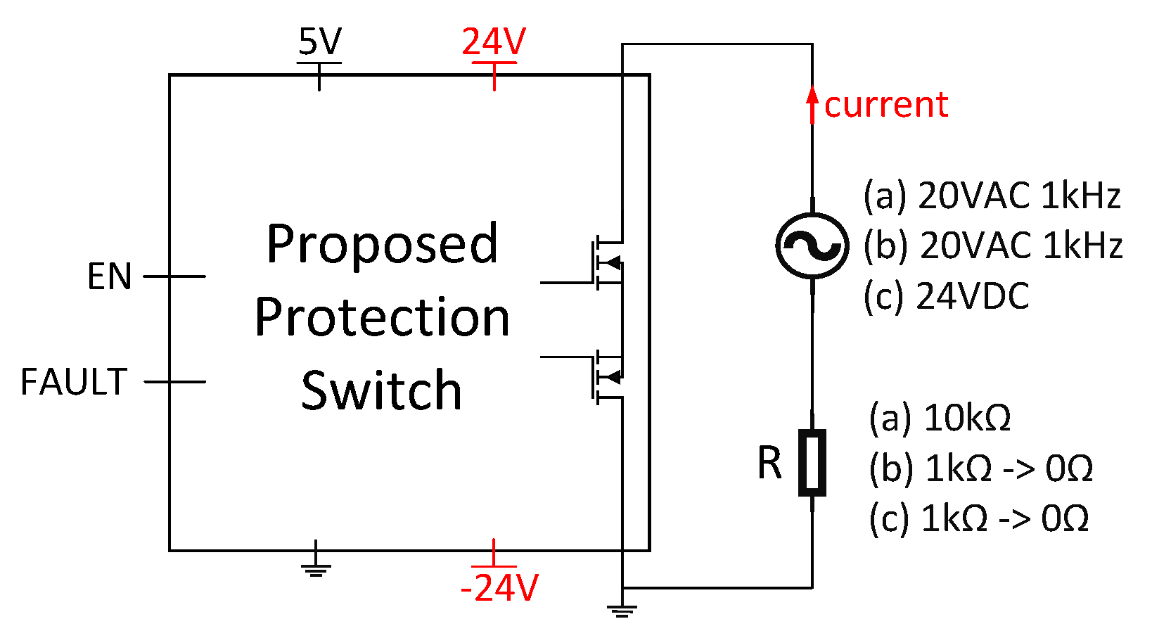
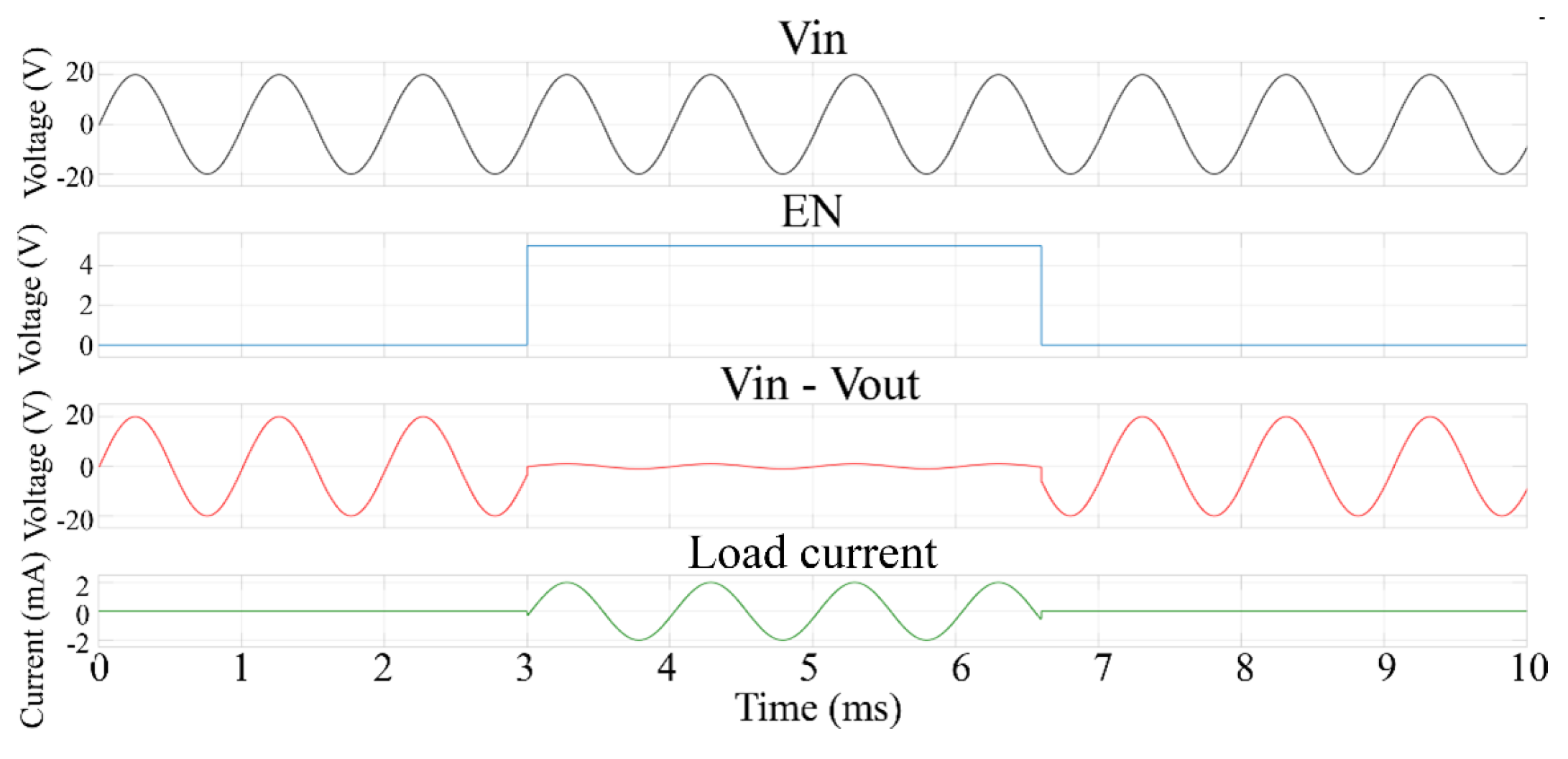
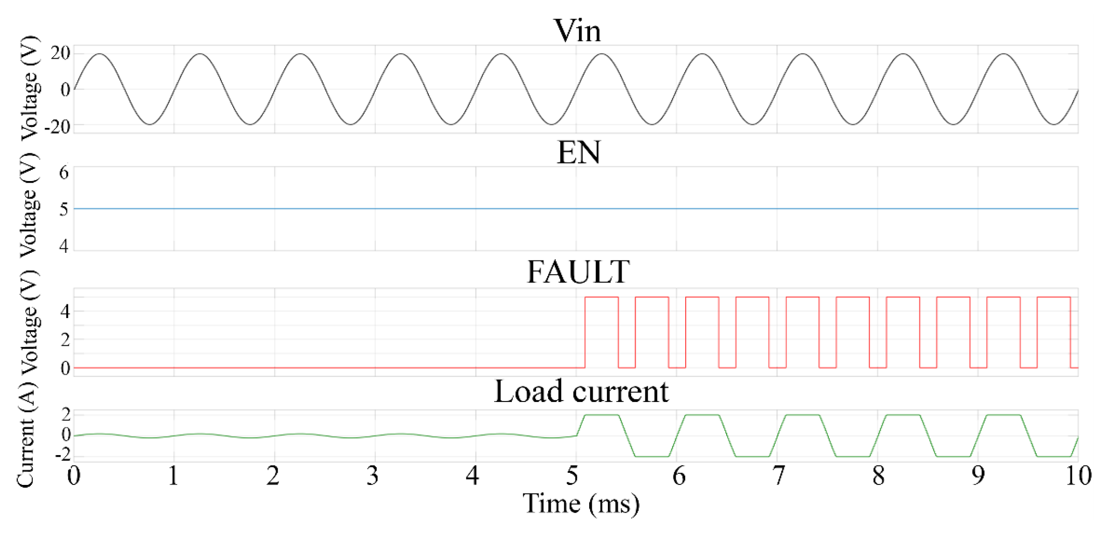
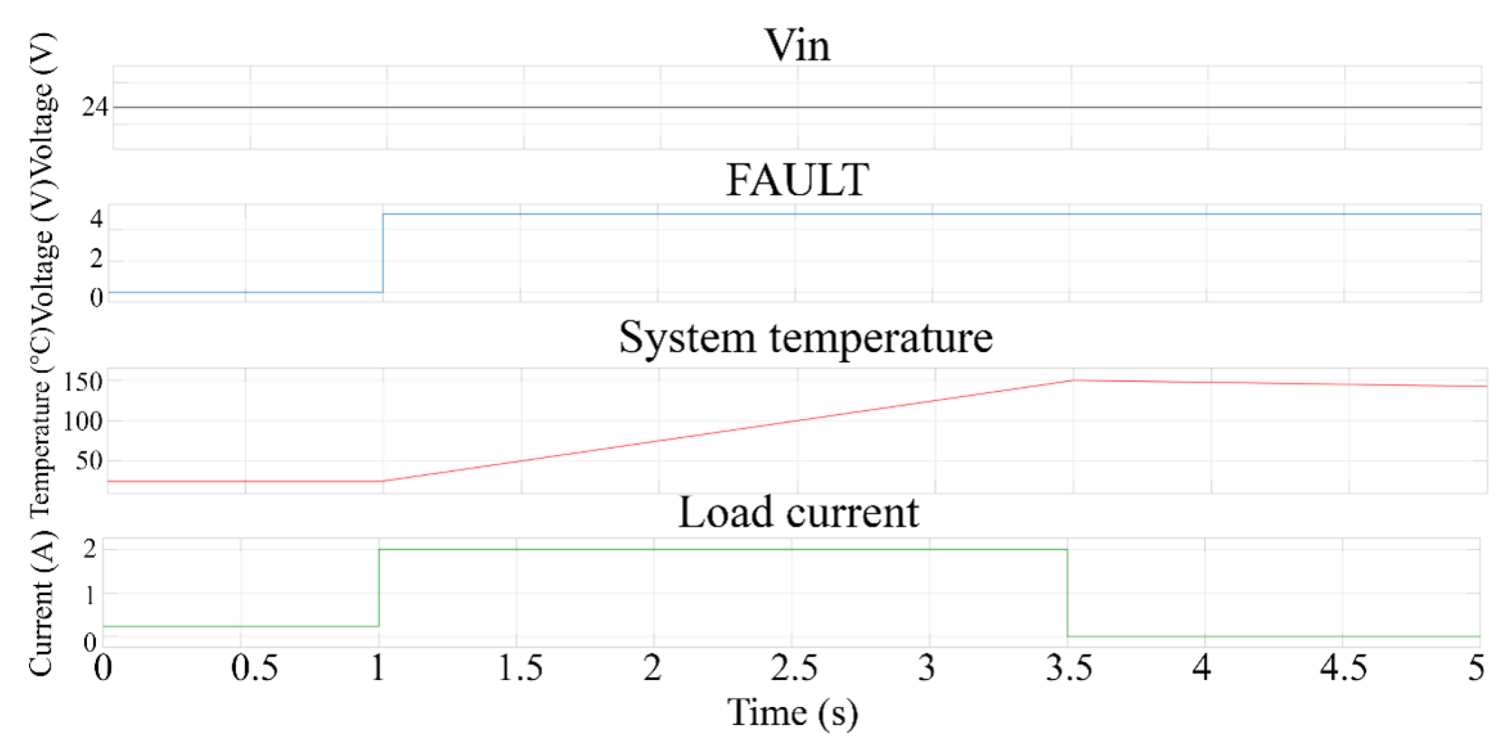
Section 4 then presents the architecture for a universal switch based on these building blocks and provides behavioral simulations in MATLAB/Simulink to illustrate the operational waveforms of the system.
2. Review of Available Protection Switches
This section reviews existing commercial and academic protection switch solutions, highlighting their limitations. This review establishes the need for a new universal solution that combines analog signal handling with robust current regulation and protection.
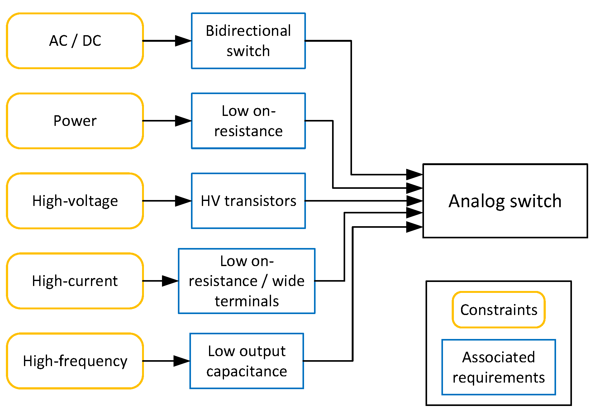
The main limitation of existing protection switch solutions is their lack of versatility. A truly universal protection switch must not only provide overcurrent protection, but also support a wide range of signal types and operating conditions. Each type of signal imposes specific constraints on the analog switch, as illustrated in
Figure 3. First, the electrical signal to be handled can be AC or DC, necessitating bidirectional operation of the switch. If the signal also carries power, its voltage and current levels can be significant. In such cases, the switch must have a low ON-resistance to minimize power loss and heat dissipation. In addition, the voltage level of the signal determines the required breakdown voltage of the transistors, which means that the chosen technology must tolerate the target voltage range. If the switch must handle a large current, low ON-resistance is again essential, and the metal interconnects and package terminals must be designed to withstand the expected current without degradation. Finally, in the case of AC signals, especially at high frequencies, the output capacitance of the switch becomes a critical factor. When the switch is open, this parasitic capacitance, formed between its terminals, can cause signal leakage or degradation. However, reducing such capacitance is often in direct conflict with achieving low ON-resistance, as increasing the transistor width (to reduce resistance) also increases parasitic capacitance. This trade-off presents a major design challenge in developing a truly universal protection switch.
Most commercially available switches with current-limiting capabilities share similar features to the solution presented in [
9]. This solution is fully integrated, supports a high current rating of 3.3 A, and includes overcurrent protection. However, it is unidirectional and cannot transfer AC signals. Solutions that offer bidirectionality for both voltage and current while maintaining sufficient power ratings are typically designed for DC applications, such as battery protection. These switches are also powered from the input terminal, as in the solution presented in [
7], which supports bidirectional current but is limited to a low voltage rating of 28 V. Transferring an analog signal is not possible while simultaneously supplying power from the same port due to potential signal disturbance. Therefore, analog switches use an independent supply pin. While some analog switches with separate supply pins offer high-voltage capability, they are not designed as autonomous protection devices and do not include overcurrent protection. The solution presented in [
10] reports a high-voltage analog switch rated at 220 V; however, it requires a supply voltage higher than the signal to operate correctly. The solution presented in [
11] does not require a high-voltage supply and supports high-voltage analog switching but is limited to only AC signals above 500 kHz. The solution in [
12] uses an isolation channel to protect the logic pins and isolate the switch MOSFET gates. This removes the need for a high-voltage supply, allowing any signal to pass through. However, this solution does not have integrated power transistors, which prevents full integration.
Several solutions have been proposed in the literature for switching high-voltage AC signals. Similar to commercial solutions, reported academic designs are typically focused either on switching high DC currents to deliver power or on handling low-current signals without overcurrent protection, making them unsuitable for this work. Most overcurrent protection schemes in high-power designs operate by opening the switch during a fault rather than clamping the current. For example, the solution in [
6] presents a monolithic protection circuit capable of withstanding high voltages up to 200 V and high currents exceeding 4.4 A. However, the switch is unidirectional and functions only as a circuit breaker, without actively limiting the current. Clamping the current, rather than completely disconnecting it, offers several advantages: faster recovery when the fault clears, continued current delivery during the fault, and avoidance of a complete shutdown during brief overcurrent events. The solution presented in [
13] features bidirectional operation with high-voltage and high-current capabilities. However, it is bulky and intended solely for power transfer, as the circuit is powered from between the switch terminals.
Solutions in [
6,
13] utilize GaN-based switches, which require specialized GaN processes. This complicates the design, as GaN technologies are not yet as mature as silicon Bipolar-CMOS-DMOS (BCD) technologies [
6]. High-voltage analog switches have also been developed using silicon-on-insulator (SOI) processes to meet the required isolation levels [
5,
6]. These solutions are fully integrated and do not require a high-voltage supply. The work in [
5] focuses on small switches that can be arranged in an array to interface ultrasonic transducers. In contrast, [
14] presents a single switch with low ON-resistance that operates without a high-voltage supply. However, these designs are limited to working with AC signals, as they rely on input voltages that fluctuate between positive and negative values to maintain gate control of switching transistors. Moreover, they do not include overcurrent protection.
3. Implementation Techniques for Protection Switch Blocks
This section presents the general high-level structure of a protection switch to clarify its overall operation. For each high-level block, the most suitable implementation techniques are explored through a review of previously proposed solutions. The objective is to identify proven techniques and assess their applicability to support the proposed design introduced in
Section 4.
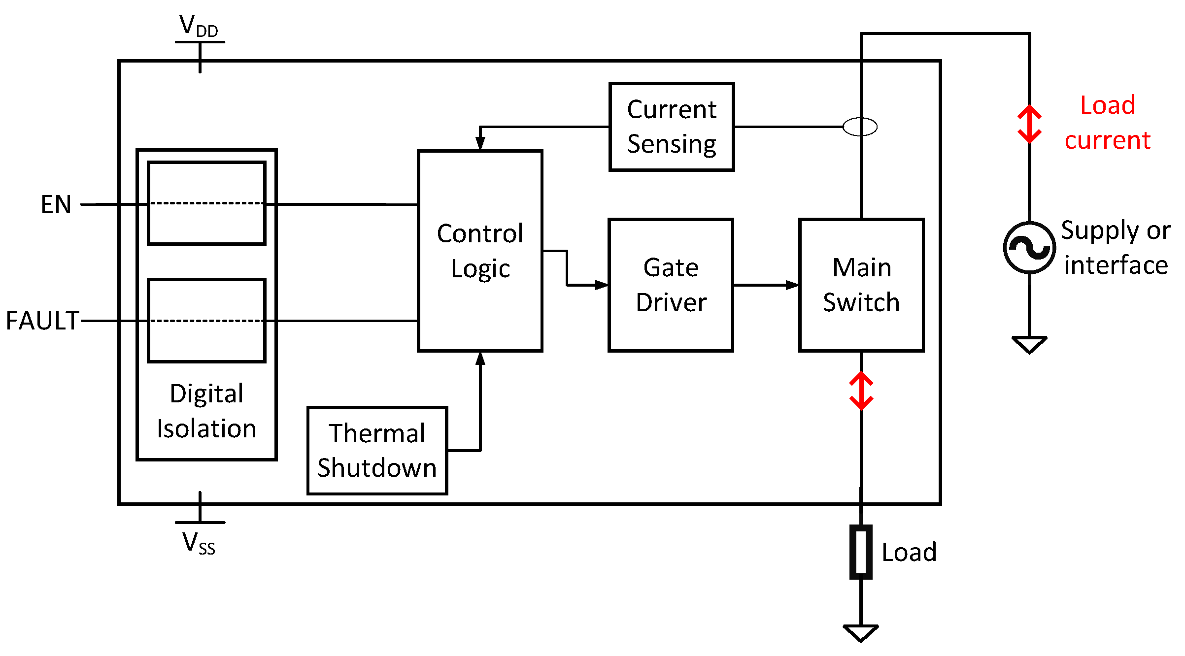
To implement a proper protection switch, the circuit must have the following components:
A main switch (MS);
A gate driver;
A current sensing mechanism;
A digital isolation scheme on the input pins;
A control logic module;
A thermal shutdown mechanism.
Figure 4 shows a high-level block diagram of a typical protection switch. During normal operation, the switch connects an electronic interface to its corresponding load, allowing current to flow through the main switch (MS) in both directions. When this current exceeds a specific threshold, the current sensing circuit detects the overcurrent, and the control logic responds by adjusting the gate drive voltage, putting the MS in a partially ON state to limit the passing current. Moreover, if the system temperature rises beyond a certain point, the control logic turns OFF the MS to prevent damage. The EN pin allows an external controller to send a command to turn the switch ON or OFF. The FAULT pin is pulled high when an overload or overheating problem is detected. In this type of operation, the protection is autonomous while the EN pin is pulled high, requiring no external intervention and allowing for easy integration.
A proper high-voltage process is essential for implementing a protection switch capable of switching or limiting high voltages. Recent implementations often use Gallium Nitride (GaN) [
6,
15] or Silicon Carbide (SiC) [
16] components due to their fast switching, low ON-resistance, and high voltage ratings. However, these technologies are more expensive and less mature than standard BCD processes. In this work, we will consider implementation using a standard SOI process.
3.1. Main Switch
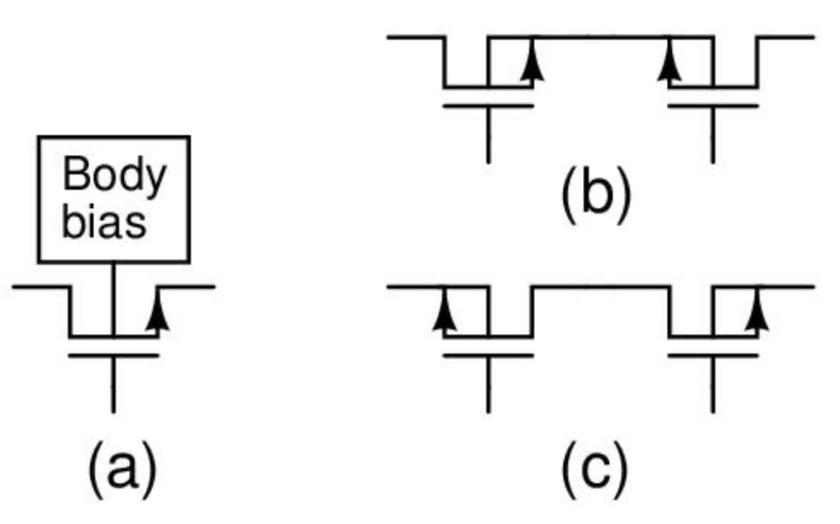
The role of the MS is to allow current to flow between its terminals in both directions during normal operation and to isolate them when a fault occurs or when the interface requests the switch to open. Therefore, in a bidirectional current path, the MS must block current and withstand high-voltage drops in both polarities while having a low ON-resistance. Several solutions have been proposed in the literature to implement the MS using BCD processes. One approach involves four-terminal devices [
17], as shown in
Figure 5a, which offer good resistance per die area, since they use only a single transistor. Compared to using two transistors in series, this solution reduces the die area by a factor of 4, as each of the two transistors would need to have half the resistance of the four-terminal device (i.e., double the width) to achieve the same total resistance. However, a symmetrical transistor and a sufficient body bias are required to prevent latchup. In SOI processes, the body terminal can be isolated to avoid this issue. Another common approach uses back-to-back connected MOSFETs, in either a common drain configuration [
9] or a common source configuration [
18], as shown in
Figure 5b and
Figure 5c, respectively. These are widely adopted to achieve bidirectionality using asymmetrical transistors with intrinsic reverse polarity diodes [
19]. Among the two, the common source configuration is more prevalent as it requires a single gate driver to control both MOSFETs.
Several high-voltage devices are available in standard BCD processes, notably thick-oxide MOSFETs and laterally diffused MOSFETs (LDMOSs) [
20]. Thick-oxide MOSFETs are generally symmetrical, but their maximum drain-to-source voltage is limited, preventing them from blocking high voltages in standard processes. In contrast, LDMOSs offer very high voltage ratings, exceeding 300 V in some cases [
21], but they are asymmetrical and require their body and source to be shorted. This constraint rules out the use of four-terminal solutions, making it necessary to use two back-to-back connected MOSFETs. To support both high voltage across the MS terminals and high load current, the use of large super junction MOSFETs is recommended. These devices offer the best balance between voltage rating and ON-resistance without resorting to specialized processes such as the use of GaN or SiC [
22].
The MS must be appropriately sized for the targeted application. The transistors forming the MS should be sufficiently wide to achieve the desired low ON-resistance. However, increasing the size of the transistors also increases the output capacitance of the switch, which is the equivalent capacitance between its terminals when it is OFF. This introduces a trade-off between AC signal integrity and high-frequency isolation.
3.2. Gate Driver
The gate driver’s role is to control the MS gate to regulate current flow under the supervision of the control logic. The gate driver must respond to shutdown events such as a low EN signal, an overcurrent event, or an overheating event. It must also be protected against high voltages present at the source terminal and be able to hold the MS in the ON state indefinitely without downtime. To achieve a universal solution, we cannot make any assumptions about the devices connected to the switch terminals. Therefore, the gate current path must be isolated; it must not flow through one of the MS terminals, as any transient or steady-state current from the gate driver through the switch terminals could disturb the signal or disrupt system operation, depending on the load type. The large signal swing and the bidirectional nature of the MS make the gate driver design particularly challenging. To drive a back-to-back common source configuration, the gate-to-source capacitance (
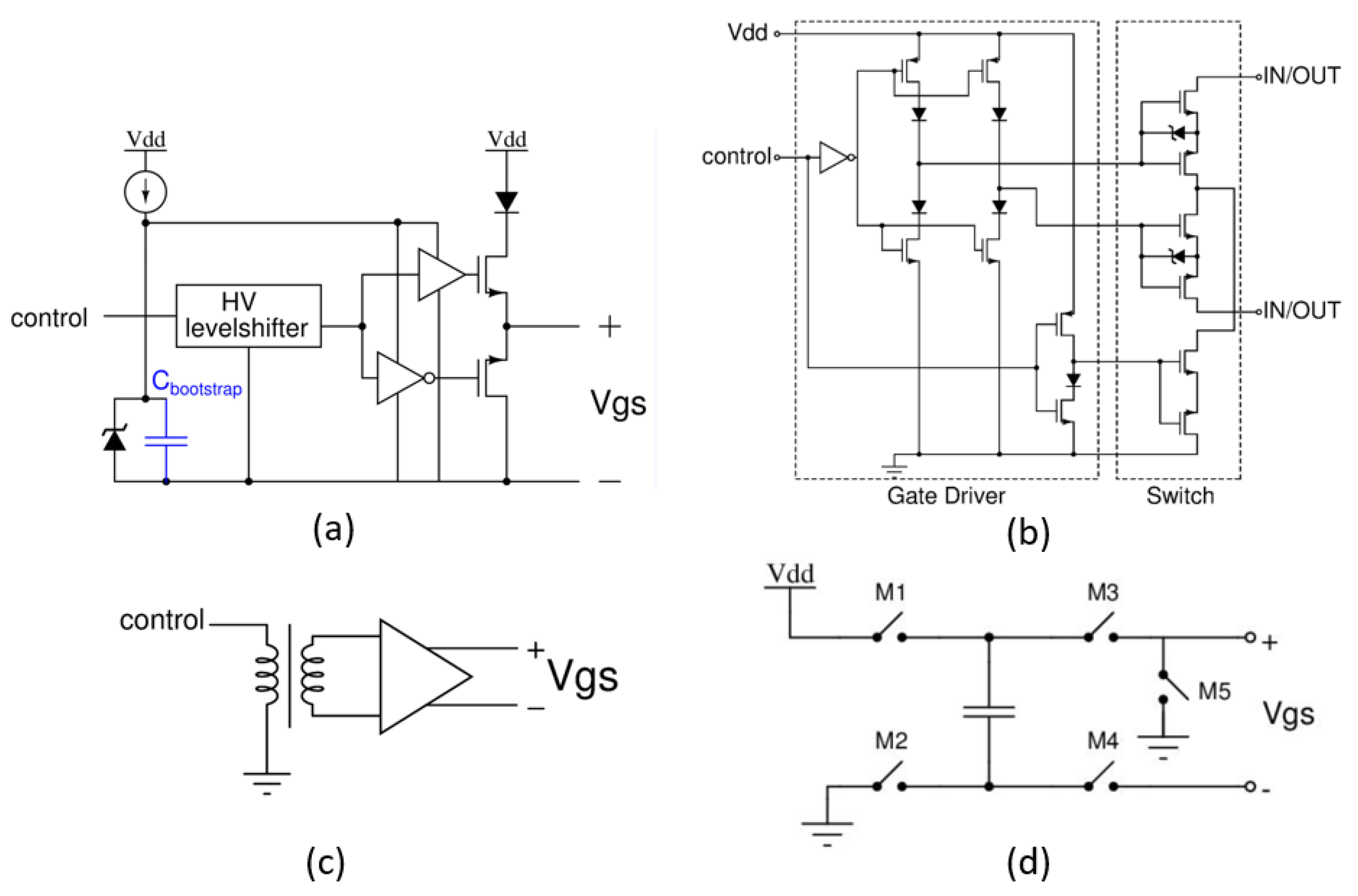
) must keep its charge to maintain the ON state of the MOSFET, even if the signal voltage swings above the supply voltage. Due to the bidirectionality, it is impossible to assume a known or fixed instantaneous voltage on any of the MS terminals. Thus, the gate driver must “float” and be referenced to the common source connection. A commonly used floating gate driver configuration consists of a bootstrapped capacitor coupled with a high-voltage level shifter, as shown in
Figure 6a [
23]. However, this solution requires a symmetrical high-voltage supply, as found in numerous commercial ICs [
24], which increases power consumption and complicates switch integration.
Other solutions exist, such as the one presented in
Figure 6b [
14], which is a compact implementation that does not require a high-voltage supply. However, it charges and discharges the gate through the switch terminals before isolating it to maintain the charge. This method is only possible if at least one terminal is connected to a low potential during charging, which limits the application range of the switch. It is therefore unsuitable for protection circuits, as it requires a supply voltage lower than the minimum signal amplitude to force the switch open, ultimately necessitating a high-voltage supply. Another approach involves using a transformer to power the gate driver, as shown in
Figure 6c. This method ensures proper gate-to-source control and provides full isolation between the low-voltage logic and the high-voltage switch [
12,
13,
16,
25]. However, it has several drawbacks: it occupies a large die area, generates electromagnetic interference (EMI), and increases power consumption. Because transformers can only transfer AC power, both signal and power must be modulated at high frequencies, which further contributes to increased power consumption. As a result, this solution is mainly used to drive half-bridge configurations in high-voltage motor control applications where galvanic isolation is essential. A more compact and widely used solution is the bootstrapped switch [
26], shown in
Figure 6d, which is often used in sample-and-hold circuits [
27]. This technique utilizes a capacitor independently charged through transistors M1 and M2 and then connected across the gate and source terminals of the MOSFET via M3 and M4 to charge
. One drawback of this technique is that the bootstrap capacitance (
) must be significantly larger than the gate capacitance or charged to a much higher voltage. This is due to charge sharing; only a fraction of the charge reaches
unless
. High-voltage, low-resistance MS devices typically have a large gate capacitance, which means that a large
is needed, which could require multiple charging cycles if
is not sufficiently large. Another limitation of the bootstrap capacitor approach is gate leakage current, which gradually discharges
over time. This leakage must be compensated for by periodically reconnecting to
, especially when the switch remains on for a long time. These drawbacks explain why the bootstrapped switch is mainly used in sample-and-hold circuits, where transistors are relatively small and do not remain closed for long periods.
Figure 6.
Possible gate driver solutions: (
a) bootstrap capacitor and high-voltage level-shifter [
23], (
b) isolated high-voltage level-shifter [
14], (
c) transformer-based isolated gate driver [
16], and (
d) bootstrapped switch [
26].
Figure 6.
Possible gate driver solutions: (
a) bootstrap capacitor and high-voltage level-shifter [
23], (
b) isolated high-voltage level-shifter [
14], (
c) transformer-based isolated gate driver [
16], and (
d) bootstrapped switch [
26].
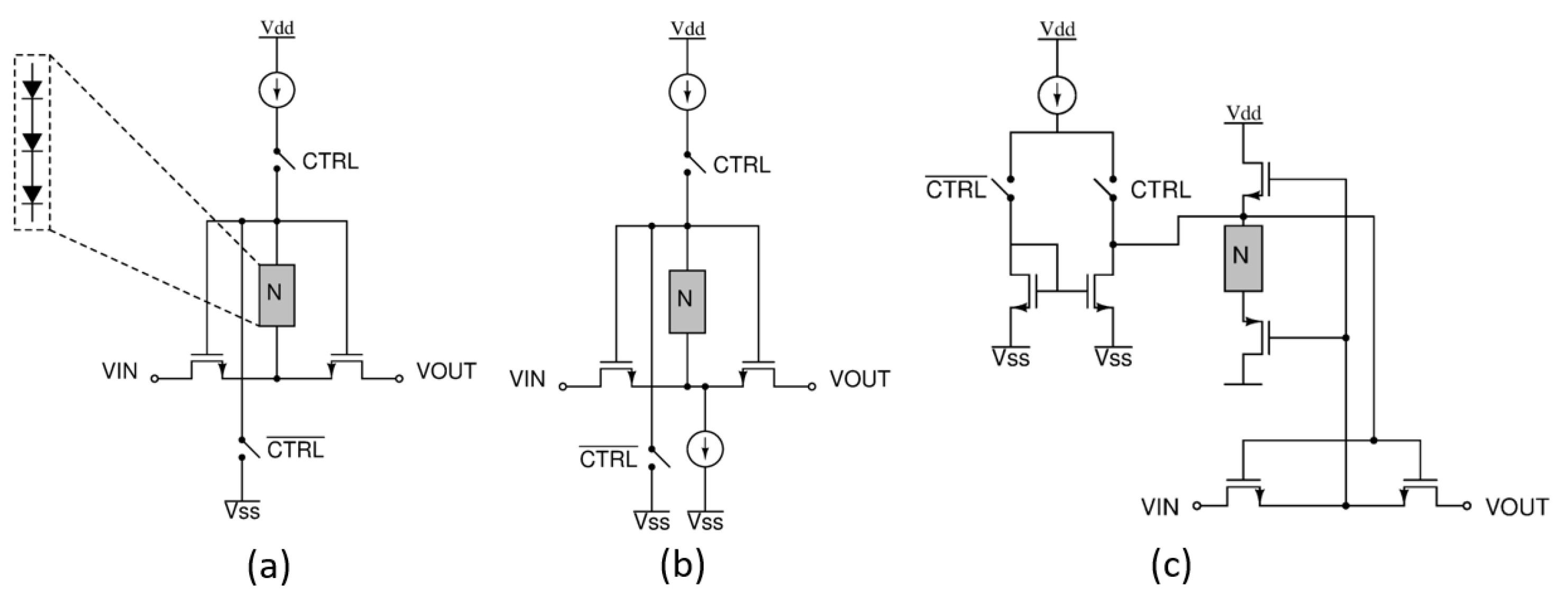
Another solution is presented in [
18] and uses the clamping network technique. The basic idea is illustrated in
Figure 7a, where a current source and a clamping network are used to generate the appropriate
voltage for the MS. Several components can be used to implement the clamping network; however, the most common topologies rely on diodes or diode-connected MOSFETs [
28]. The main issue with the driving technique presented in
Figure 7a is that the driver current flows through the MS terminals, which, as previously mentioned, is unsuitable for switching AC signals. The structure in
Figure 7b fixes this problem by using an additional current source to sink the current at the source terminal [
29]. However, any mismatch between the two current sources can still result in a small undesired current flowing through the MS terminals. More recent approaches solve this by using a source-follower MOSFET to completely isolate the driver path from the MS current path, as shown in
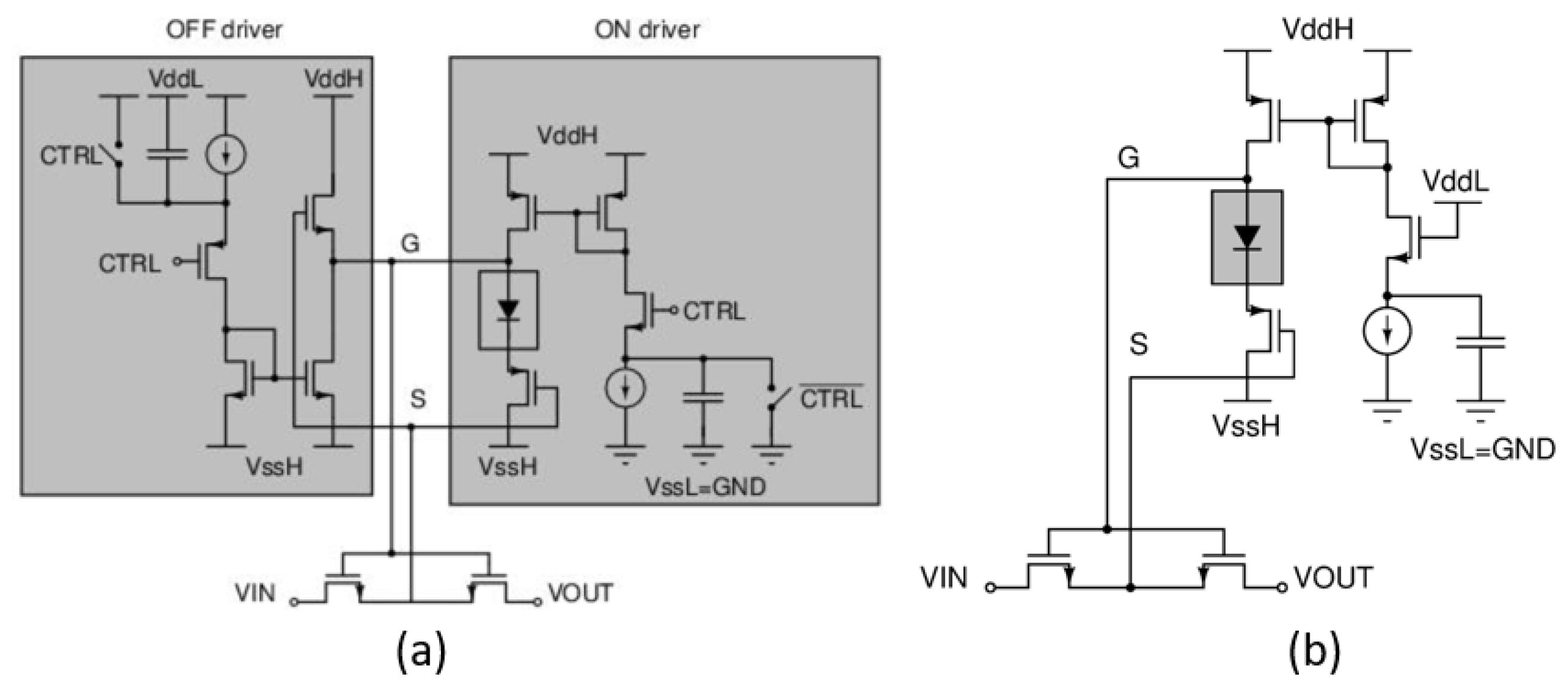
Figure 7c. Building on the clamping network technique, the solution presented in [
18], illustrated in
Figure 8, uses a dual source-follower structure with separate ON- and OFF-driving circuits. This design offers a better trade-off between switching speed and static power consumption by decreasing the current injected into network N after switching, thereby reducing overall power consumption. The structure provides a good compromise between power consumption, switching speed, and implementation complexity. However, it still requires a high-voltage supply with a voltage range exceeding that of the signal passing through the switch.
All the gate driver solutions reviewed thus far are designed to turn the MS ON or OFF fully. However, in this work, the goal is to actively limit the current once it exceeds a certain threshold. To achieve this without adding additional circuitry in series with the MS, gate charge control is often used [
9]. This involves modifying the chosen gate driver so that it is controlled by a feedback signal from the current sensing circuit. In practice, this can be achieved by replacing the fixed supply voltage or current source, in the presented topologies, with a voltage-controlled voltage source or a voltage-controlled current source, based on the sensed current level.
3.3. Current Sensing
The current sensing circuit provides current feedback to the control logic circuitry. The selected technique should be accurate, reliable, and have minimal impact on the transmitted signal. It must also present low impedance in series with the MS in the current path to avoid signal attenuation. Current sensing techniques suitable for integrated solutions are discussed in more detail in [
30,
31]. Here, we summarize the most relevant techniques.
3.3.1. Series Shunt
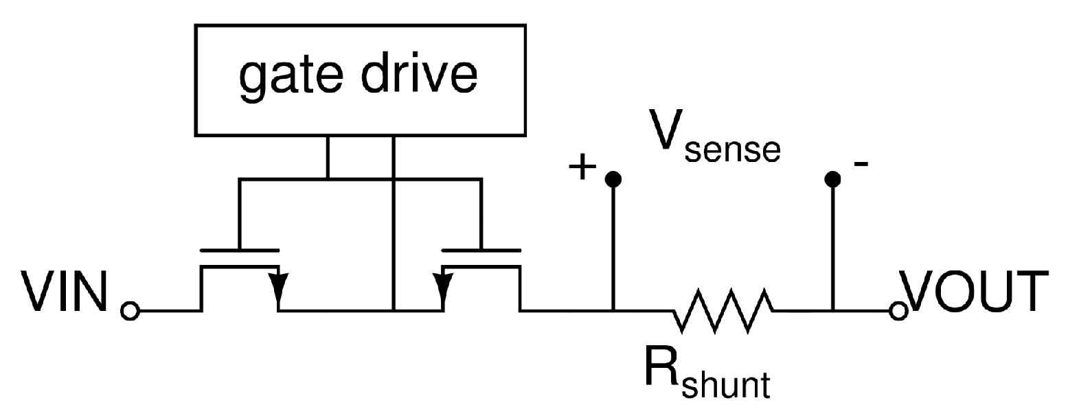
The most widely used approach is the series shunt current sensing illustrated in
Figure 9. It uses a small detection resistor to produce a voltage drop proportional to the current flowing through it. This voltage drop is then amplified using a differential amplifier to interface with the control logic. Although process variations can introduce some uncertainty in the resistor value, this method generally offers good accuracy and bandwidth. The main drawbacks are the added ON-resistance and power dissipated across the resistor, which are limiting factors in low-power applications.
3.3.2. Sensing
This method is similar in principle to the series shunt sensing approach, but it directly uses the power MOSFET’s own ON-resistance as the sensing element, eliminating the need for an external resistor. This improves efficiency and signal quality. The expression for the MOSFET’s ON-resistance in the ohmic region is given by (
1) [
30]:
where
L is the channel length,
W is the channel width,
is the carrier mobility,
is the oxide capacitance per unit area,
is the gate-to-source voltage, and
is the threshold voltage.
is highly sensitive to temperature, which significantly influences
, and to process variations. The total variation of
can reach up to 100% of its nominal value, making this technique highly inaccurate in standard processes [
30].
3.3.3. SenseFET
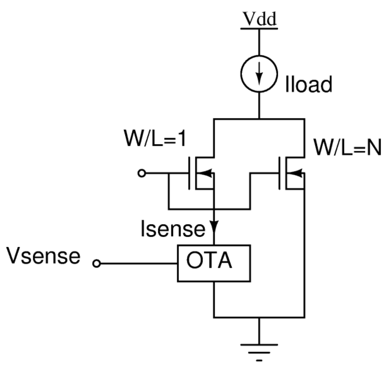
This technique uses matched MOSFET cells that share common terminals. Because the ON-resistance of individual cells within a power MOSFET is well matched, a small subset can be routed to a separate sense pin to accurately mirror the current flowing through the main cells. The current ratio
N is equal to the ratio of the number of cells in the main and sensing paths, as shown in
Figure 10, and is typically on the order of 1000 [
32]. The mirrored current can be sensed using either a shunt resistor or a transimpedance amplifier. As long as the sensing resistance is small compared to the SenseFET’s ON-resistance, this technique can be considered lossless, with the sensing current approximating the load current divided by
N. The advantages of SenseFETs include eliminating additional series resistance and good stability across temperature and process variations. The two main drawbacks are the sensing voltage spikes that can occur during the switching event and the constraints on the MOSFET layout. While turn-on spikes can be mitigated with a low-pass filter, doing so also reduces the bandwidth. Additionally, achieving high accuracy requires the use of a Kelvin connection layout and placing the sensing interface (e.g., the OTA in
Figure 10) close to the SenseFET.
3.4. Digital Isolation
If the protection switch fails, the interface must still be protected from the high-voltage signals at the output. Therefore, digital isolation should be present on the interface pins, as illustrated in
Figure 4. In the presented architecture, two isolation channels are required, one to protect the EN pin and the other to protect the FAULT pin. These channels can be implemented using either a single modulated link [
33] or two separate isolation links [
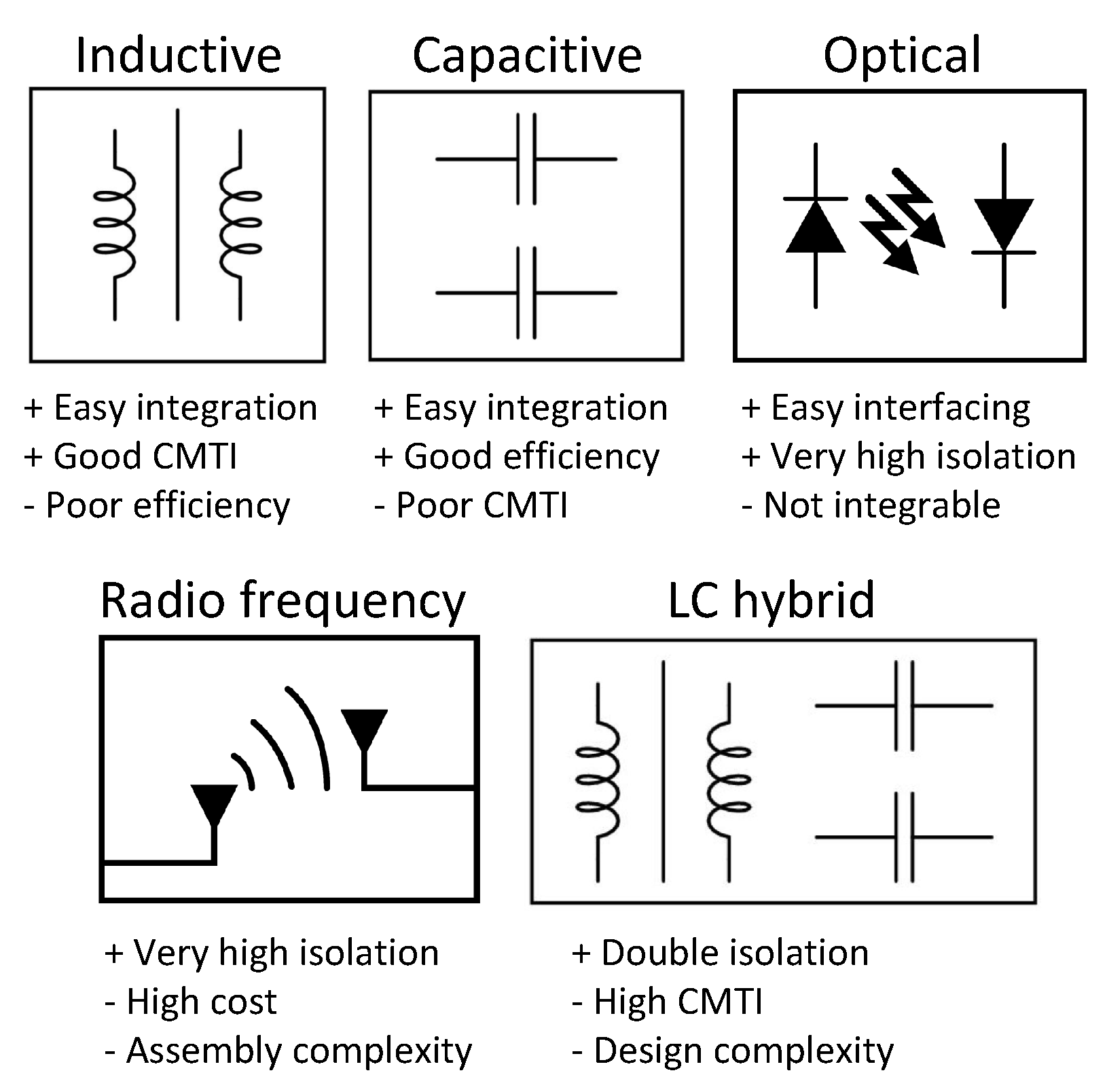
34], which is the most common approach. The digital isolation must be able to withstand the absolute maximum voltage of the switch. Three types of isolation links are commonly used for this purpose: optocoupler, inductive link, and capacitive link [
35]. Other alternatives exist, such as RF isolators [
36] or hybrid LC isolators [
37], but they greatly complicate the design and occupy a large die area. The commonly available solutions for implementing digital isolation are illustrated in
Figure 11.
Optocoupler-based solutions offer high isolation ratings (above 5 kV) and are easy to use. However, they are typically made using GaAs technology and cannot be integrated into standard CMOS processes. As a result, they are not fit for this work, which targets monolithic system integration. Furthermore, optocouplers have shorter lifetimes and face reliability issues compared to other isolation methods [
38]. Inductive isolation is often based on coupled coils implemented across different metal layers to form an on-chip transformer. Although integrated transformers can generate EMI and generally exhibit poor efficiency, they offer excellent common-mode transient immunity (CMTI) and can also be used to transfer power. The implementation of coils often occupies a large die area, but recent iterations managed to keep its footprint moderated, especially for low-power applications where only data are transmitted [
39]. Capacitive isolation, by contrast, does not generate EMI, consumes less power, and generally occupies a smaller die area. However, it provides lower CMTI than inductive isolation and is less suited for low-frequency applications. Transmitting both low- and high-frequency signals requires either large capacitors or another dedicated channel for low-frequency signals. In our case, only a continuous signal needs to be transmitted, so a single modulated channel is sufficient. Common modulation schemes for capacitive coupling include ON–OFF keying (OOK), which is simple and requires minimal circuitry, and pulse polarity modulation, which is more complex but consumes less power [
40,
41].
3.5. Thermal Shutdown
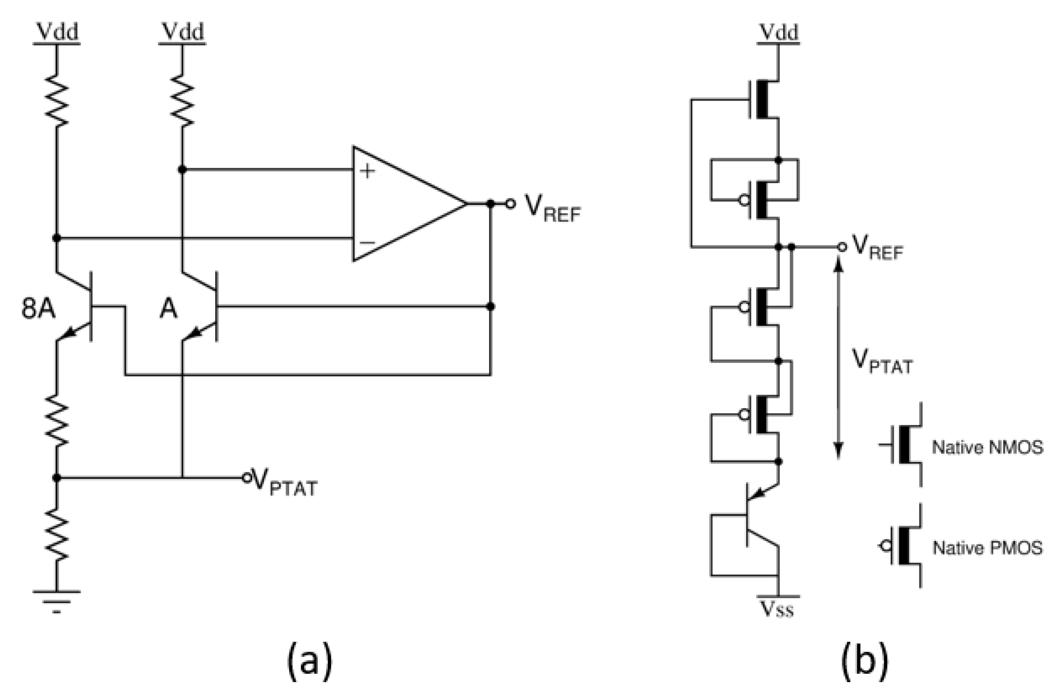
Despite limiting the current during overcurrent events, the switch must be able to automatically turn OFF if the on-chip temperature exceeds its maximum rated value due to power dissipation. Most integrated temperature sensors rely on the diode’s forward voltage or a bipolar junction transistor as a reference, since this voltage varies linearly with temperature for a fixed current. Nearly all voltage reference circuits generate both a proportional to absolute temperature (PTAT) voltage and a temperature-independent voltage. One of the most common implementations is the Brokaw reference [
42], shown in
Figure 12a. Using such a reference, the temperature sensor circuit can also serve as a voltage reference for a step-down converter, offering integration and design efficiency. A basic Brokaw reference is a suitable option due to its simplicity and wide input voltage range. Alternatively, more recent solutions may also be considered. For example, the design presented in [
43], shown in
Figure 12b, implements a hybrid bandgap and threshold voltage reference with ultra-low power consumption. When paired with a comparator for overtemperature detection, this solution can provide a very compact and low-power implementation that functions as both a voltage reference and a thermal shutdown mechanism.
5. Summary of Existing Solutions
Finally,
Table 1 summarizes the capabilities and trade-offs of the existing commercial and academic solutions, clarifying where the proposed universal architecture could address missing features if implemented in silicon. To our knowledge, no existing solution offers a fully integrated, bidirectional, high-voltage analog switch with built-in overcurrent protection. Most protection solutions are intended for DC applications, such as battery protection, and are only unidirectional, like the designs presented in [
6,
9]. These designs include overcurrent protection and support high current ratings but do not operate in both polarities. The analog switches in [
7,
13] allow bidirectional current flow but are powered through an input terminal unsuitable for conveying AC signals. In such configurations, the supply current overlaps with the signal, introducing considerable noise. Other solutions, such as those in [
12,
13], do not support full monolithic integration of the protection switch, a significant drawback, as monolithic integration improves system compactness, performance, and integration into existing applications. The solution presented in [
11] provides an isolated analog switch, but its current rating is only 5 mA, which is insufficient for many practical applications. Finally, the solutions presented in [
10,
14] both feature bidirectionality, high isolation ratings, independent supply pins, and monolithic integration; however, they lack overcurrent protection.
The presented universal solution in
Section 4 incorporates all these essential features, including overcurrent protection, into a flexible architecture that can be adapted for a range of applications. The maximum voltage and current capabilities can be adjusted by appropriately sizing the MS, based on the relevant design trade-offs. For example, using low-voltage transistors reduces the maximum voltage rating and decreases the ON-resistance per unit area, which can be a favorable trade-off in low-voltage applications. The gate driver current and the circuit’s power supply are isolated from the protection switch terminals, guaranteeing undisturbed signal transfer and enabling true analog switching. Digital isolation protects the interface from being damaged in the event of failure. Finally, a high-voltage SOI process provides the potential for full integration on a single die, as its deep trench isolation (DTI) structures support robust separation between high-voltage and low-voltage domains. This capability enables on-chip digital isolation and can reduce manufacturing cost, design complexity, and system footprint.
