Abstract
A class E inverter has presented wide application prospects in inductive wireless power transfer (WPT) systems due to its significant advantages such as high operation frequency, high power density, and low cost. However, its semiconductor power device is subjected to voltage stress several times higher than the input DC voltage, which inevitably increases the risk of overvoltage failure and limits the system power level. In this manuscript, an inductive WPT system with the pull–push class EF2 inverter is proposed to significantly decrease the voltage stress and ensure soft switching characteristic. The working principle and time-domain waveforms of the pull–push class EF2 inverter are analyzed. Moreover, the differential equations and mathematical model of the resonant parameters are investigated. Compared with the conventional class E inverter, the output power of the proposed inductive WPT system is doubled under the same input voltage. A 100 W system prototype is designed at the operating frequency of 6.78 MHz (according to the A4WP standard) and its experimental results demonstrate the effectiveness and feasibility of the analysis.
1. Introduction
Wireless power transfer (WPT) technology [1,2,3] can be widely applied in some battery-powered systems, such as consumer electronics, implantable medical devices, and electric vehicles (EVs). Properties such as ultra-lightweight and thin are favored by most customers, which means it is mandatory to improve the inductive WPT system power density. The method of increasing system operating frequency to the Megahertz-wide band has been proven to be a viable solution [4,5,6].
The operating frequency is determined by an inverter, which is an important component of the inductive WPT system. Full-bridge inverters can be used for both low-power and high-power applications [7]. However, the class E inverter [8,9] is a resonant converter that can operate at MHz operating frequency and offers higher efficiency and low cost. It is usually useful for low power applications. In recent years, it has been widely promoted and applied in inductive WPT systems [10,11,12].
Reference [13] analyzes the load-independent output characteristic of the class E inverter. Also, its ZVS operation and constant output voltage are investigated at different load conditions. To eliminate the influence of conduction resistance and parasitic capacitance of the semiconductor power device, a cascaded class E inverter is proposed in [14]. The designed prototype operates at 13.56 MHz and its peak efficiency is up to 80.19%. Reference [15] applied the class E inverter and class E rectifier to an inductive WPT system. At the air gap of 5 mm, the inductive WPT system output power and efficiency, respectively, were 0.769 W and 74.1%.
For the class E inverter, however, the voltage stress of its semiconductor power devices is up to 3.5 times of the DC input voltage [16]. This can easily lead to overvoltage failure and limit the system power level. Adding high-order resonant networks has been proven to be an effective solution to reduce the voltage stress. A class EF2 inverter [17,18,19,20] is proposed and its added LC (inductive-capacitor) resonant network parallel with the power devices can reduce the voltage stress up to 2.5 times the input voltage. Additionally, Ref. [21] proposed a class EF2 inverter based on a T-type impedance matching network. Based on the proposed topology, a 1.7 kW/6.78 MHz inductive WPT prototype is designed, and its maximum efficiency is higher than 95%. However, the high voltage stress, complex design process (due to the tuning interactions) and harsh soft switching condition of the class EF2 inverter still constrain its widespread application in inductive WPT systems.
In this manuscript, a pull–push class EF2 inverter is proposed and applied in an inductive WPT system. For the proposed pull–push class EF2 inverter, the second harmonic is eliminated to decrease the voltage stress to 1.16 times the input voltage. The topology structure, working principle and mathematical model are analyzed. And the theoretical analysis is verified using a 100 W experimental prototype.
2. Modeling and Analysis of Pull–Push Class EF2 Inverter
2.1. Topology Structure
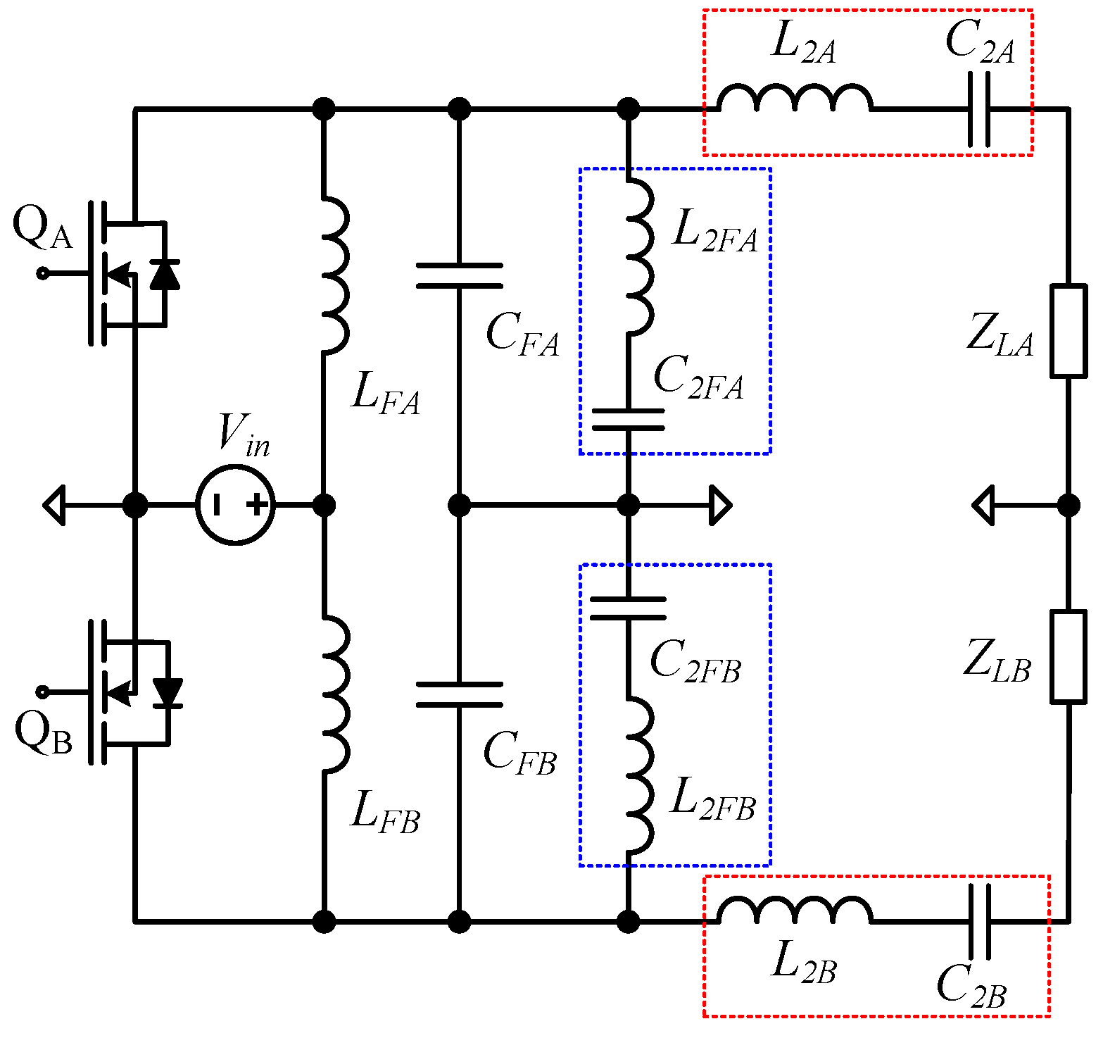
Figure 1 shows the structure of the pull–push class EF2 inverter. It is composed of the DC input voltage, choke inductors (LFA and LFB), semiconductor power devices (QA and QB), parallel connected capacitors (CFA and CFB), and resonant networks. Figure 2 shows the time-domain waveforms of the pull–push class EF2 inverter. Here, QA and QB turn on alternatively.
Figure 1.
Topology of a pull–push class EF2 inverter.
Figure 2.
Time-domain waveforms of the pull–push class EF2 inverter.
2.2. Mathematical Model of the Resonant Parameters
In Figure 1, the power devices QA and QB alternatively turn on. So, the pull–push class EF2 inverter can be equivalent to two independent class EF2 inverter to simplify the analysis of the system and the design of parameters. Figure 3 shows a class EF2 inverter, and its voltage and current waveforms are shown in Figure 4.
Figure 3.
(a) A class EF2 inverter topology and its equivalent circuits. (b) The power switch is turned on and (c) the power switch is turned off.
Figure 4.
Waveforms for optimum operation.
The power device is turned on at the time interval of (1 − D)T ≤ t ≤ T. Here, D denotes the duty cycle and T is the period. In this case, the equivalent circuit is shown in Figure 3b. And the terminal voltage of the choke inductor is equal to the input DC voltage. The current of the inductor L2F increases linearly. Moreover, one can obtain the following differential equation from Figure 3b:
The solution of Equation (1) is expressed as follows:
To avoid series resonance between the inductor L2F and the capacitor C2F, they should satisfy
By substituting Equation (2) into (1), one can obtain
From Equation (4), the voltage of capacitor C2F is always equal to 0.
When the power device is turned off, the node current is expressed as follows:
Equation (5) is equivalent to the following equation:
Here, the terminal voltage of the capacitor CF is given by
By combining Equations (6) and (7), the following differential equations are obtained:
In addition, Equation (8) is equivalent to
Using Equation (9), variables 1, 1, 2, 2 and A1, A2, A3, A4, A5 can be defined and applied to analyze the resonant parameters of the class EF2 inverter. The characteristic root of Equation (9) can be expressed as
Then, is given by
From (3) and (4), one can obtain vC2F(0) = vC2F(T) = 0 and iC2F(0) = iC2F(T) = 0. Therefore, the following expression can be obtained:
To obtain ZVS and ZDVS characteristics, the following equation should be satisfied:
Also, the input current is given by
Its solutions are as follows:
By substituting the condition of vC2F(0) = 0 into Equation (2), we can obtain
Here,
And
Then, the resonant parameters of the class EF2 inverter are given by
3. Wireless Power Transfer System with Pull–Push Class EF2 Inverter
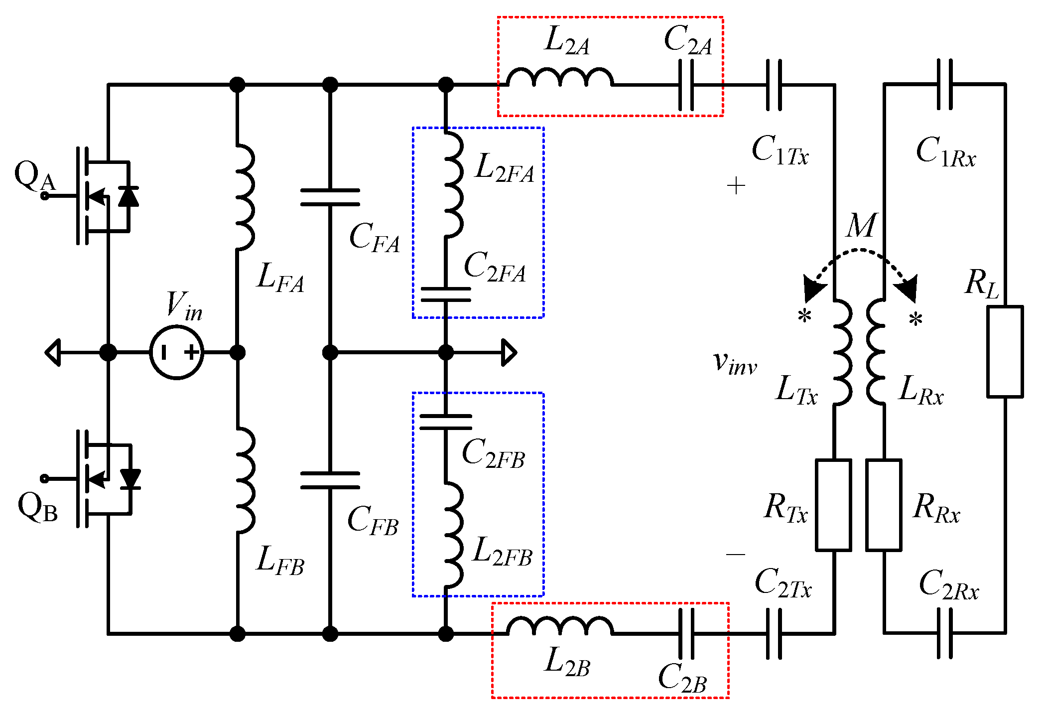
Figure 5 shows the SS (series–series) compensated inductive WPT system with the proposed pull–push class EF2 inverter. LTx and LRx are the self-inductance of the Tx and Rx coils. CTx and CRx are the compensation capacitors at the Tx and Rx sides. M is the mutual inductance between the Tx and Rx coils. And there is no issue of electromagnetic compatibility. RTx and RRx are the ESR (equivalent series resistance) of the Tx and Rx coils. ITx and IRx represent the currents flowing through the Tx and Rx coils. The load is denoted as RL.
Figure 5.
SS compensated inductive WPT system with pull–push class EF2 inverter.
According to the Kirchhoff’s Voltage Law (KVL), Figure 5 can be modeled as
The currents flowing through the Tx and Rx coils can be solved as follows:
Here, and .
Then, the input and output power can be given by
The system efficiency is as follows:
The following resonant conditions can be designed:
The efficiency is simplified as follows:
4. System Prototype and Experimental Results
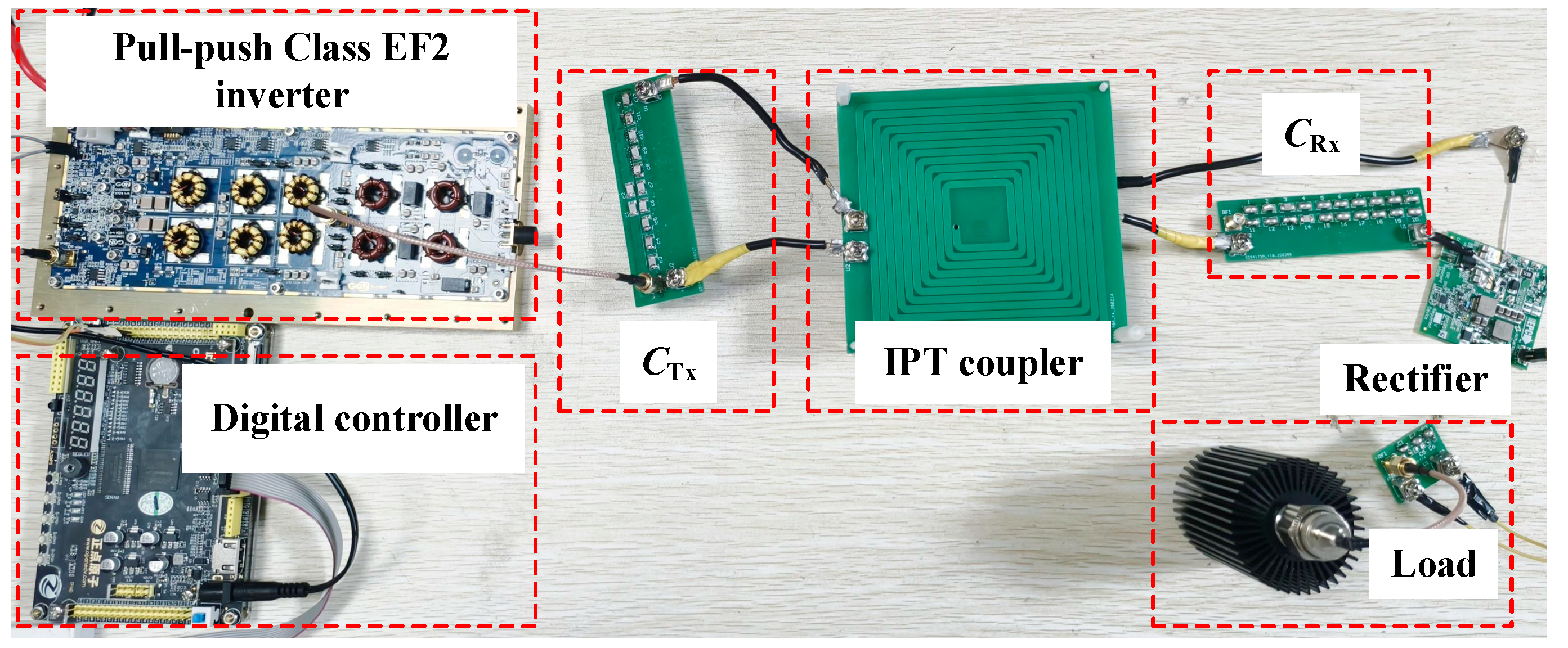
A 6.78 MHz inductive WPT system based on the proposed pull–push class EF2 inverter is built and shown in Figure 6. And its parameters are given in Table 1. Specifically, the PCB (Printed Circuit Board) coil is designed for the IPT coupler. Its turn number is 10 and the coil size is 10 cm × 10 cm. The air gap between the Tx coil and Rx coil is about 1 cm. GS66504B-TR (Infineon Technologies, Mansfield, Texas USA) is a GaN-on-Silicon transistor with fast switching bottom cooling and low thermal resistance, which is applied for the power switches (QA and QB). The KEMET MLCC capacitor is used for CTx and CRx.
Figure 6.
The system prototype.
Table 1.
System parameters.
Figure 7 shows the gate driver of the semiconductor power devices QA and QB. The measured waveforms align with the results of the analysis where the two switches are turned on alternatively.
Figure 7.
The measured gate driver of the semiconductor power devices.
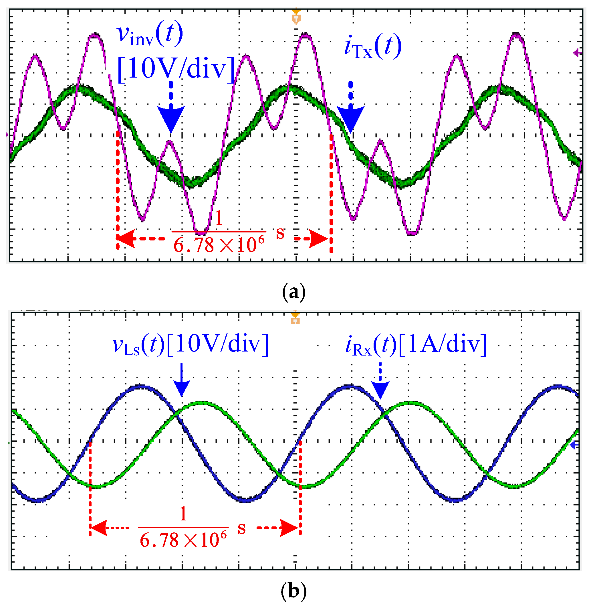
Figure 8a shows the measured output voltage of the pull–push class EF2 inverter and the current flowing through the Tx coil. The waveforms are similar to those displayed in Figure 2. The voltage slightly reduces the current, which ensures soft switching characteristics. In addition, the induced voltage of the Rx coil and output current are presented in Figure 8b. They are both sinusoidal waves and their phase difference is about π/2. Figure 9a shows the measured waveforms when the load resistance is decreased from 50 Ω to 25 Ω and Figure 9b shows the measured vinv(t) and iTx(t) when there is a 1 cm misalignment between the Tx and Rx coils. The measured efficiency of the inductive WPT system by a HIOKI power meter is shown in Figure 10. The peak efficiency is up to 90.1%. The comparison of the proposed WPT system with the pull-push class EF2 inverter with the conventional topologies in term of efficiency, rated output power, etc. is shown in Table 2. It can be seen that the proposed system has significantly advantage, especially in terms of the voltage stress of the power device.
Figure 8.
Experimental results. (a) Inverter output voltage vinv(t) and current flowing through the Tx coil iTx(t) and (b) induced voltage of the Rx coil and output current.
Figure 9.
Measured vinv(t) and iTx(t) when (a) the load resistance is changed from 50 Ω (rated load) to 25 Ω and (b) there is a 1 cm misalignment between the Tx and Rx coils.
Figure 10.
Measured peak efficiency.
Table 2.
Comparisons between this work with the conventional inductive WPT system.
5. Conclusions
This manuscript proposed a pull–push class EF2 inverter. Compared with the conventional class E inverter, the voltage stress of the semiconductor power device decreases from 2.5 times the input DC voltage to 1.16 times, which will significantly reduce the risk of overvoltage failure and increase the system power level. Furthermore, an inductive WPT system based on the proposed pull–push class EF2 inverter is analyzed. The mathematical model of the currents flowing through the Tx and Rx coils, output power and efficiency are investigated. A 6.78 MHz inductive WPT prototype is built, and its experimental results verify the theoretical analysis.
Author Contributions
Y.W. and J.L. take primary responsibility for conceptualizing the manuscript, developing the structure, and writing most of the content. J.K. and C.L. have made significant contributions to the literature review and analysis, performing the numerical calculations for the suggested experiment. Z.C., J.M. and P.C. carried out the experiments. All authors have contributed to the revision and refinement of the manuscript ensuring its clarity, coherence, and accuracy. We would like to express our gratitude to each author for their dedication, hard work, and invaluable contributions to the manuscript. All authors have read and agreed to the published version of the manuscript.
Funding
This work was supported by the research project funding from China Three Gorges Corporation under Grant SXKCY2024012.
Data Availability Statement
The original contributions presented in this study are included in the article. Further inquiries can be directed to the corresponding author.
Conflicts of Interest
Authors Y.W., J.K., C.L., Z.C., J.M. and P.C. were employed by China Three Gorges Corporation. The remaining authors declare that the research was conducted in the absence of any commercial or financial relationships that could be construed as a potential conflict of interest.
References
- Alotaibi, F.M. Optimized Coupling Coil Geometry for High Wireless Power Transfer Efficiency in Mobile Devices. J. Low Power Electron. Appl. 2025, 15, 36. [Google Scholar] [CrossRef]
- Niu, S.; Jia, Q.; Hu, Y.; Yang, C.; Jian, L. Safety Management Technologies for Wireless Electric Vehicle Charging Systems: A Review. Electronics 2025, 14, 2380. [Google Scholar] [CrossRef]
- Chai, L.; Song, C.; Lu, J. A Coaxial and Coplanar Wireless Slipring for Multi-Axis Robot Manipulators. Electronics 2022, 11, 2352. [Google Scholar] [CrossRef]
- Liu, M.; Qiao, Y.; Liu, S.; Ma, C. Analysis and Design of a Robust Class E2 DC–DC Converter for Megahertz Wireless Power Transfer. IEEE Trans. Power Electron. 2017, 32, 2835–2845. [Google Scholar] [CrossRef]
- Jawad, A.M.; Nordin, R.; Jawad, H.M.; Gharghan, S.K.; Abu-Samah, A.; Abu-Alshaeer, M.J.; Abdullah, N.F. Wireless Drone Charging Station Using Class-E Power Amplifier in Vertical Alignment and Lateral Misalignment Conditions. Energies 2022, 15, 1298. [Google Scholar] [CrossRef]
- Li, Q.; Duan, S.; Fu, H. Analysis and Design of Single-Ended Resonant Converter for Wireless Power Transfer Systems. Sensors 2022, 22, 5617. [Google Scholar] [CrossRef] [PubMed]
- Detka, K.; Górecki, K. Wireless Power Transfer—A Review. Energies 2022, 15, 7236. [Google Scholar] [CrossRef]
- Ashique, R.H.; Maruf, M.H.; Sourov, K.M.S.H.; Islam, M.M.; Islam, A.; Rabbani, M.; Islam, M.R.; Khan, M.M.; Shihavuddin, A. A Comparative Performance Analysis of Zero Voltage Switching Class E and Selected Enhanced Class E Inverters. Electronics 2021, 10, 2226. [Google Scholar] [CrossRef]
- Ashique, R.H.; Arif, M.S.B.; Bhatti, A.R.; Al Mansur, A.; Maruf, M.H.; Shihavuddin, A. The ZVS Class E/F3 Inverter Using Piezoelectric Transformers for Energy Extraction. Electronics 2023, 12, 2118. [Google Scholar] [CrossRef]
- Xiao, W.; Shen, R.; Zhang, B.; Qiu, D.; Chen, Y.; Li, T. Effects of Foreign Metal Object on Soft-Switching Conditions of Class-E Inverter in WPT. Energies 2018, 11, 1926. [Google Scholar] [CrossRef]
- Zhang, S.; Zhao, J.; Wu, Y.; Mao, L.; Xu, J.; Chen, J. Analysis and Implementation of Inverter Wide-Range Soft Switching in WPT System Based on Class E Inverter. Energies 2020, 13, 5187. [Google Scholar] [CrossRef]
- Maji, S.; Etta, D.; Afridi, K.K. Comparison of Resonant Inverter Topologies for Multi-MHz Wireless Power Transfer Systems. In Proceedings of the 2024 IEEE Energy Conversion Congress and Exposition (ECCE), Phoenix, AZ, USA, 20–24 October 2024; pp. 2187–2192. [Google Scholar] [CrossRef]
- Aizawa, S.; Yasuda, T.; Uchida, A.; Luo, W.; Wei, X.; Sekiya, H. Load-Independent Class-E Inverter with a Class-D Rectifier. In Proceedings of the 2023 12th International Conference on Renewable Energy Research and Applications (ICRERA), Oshawa, ON, Canada, 29 August–1 September 2023; IEEE: Piscataway, NJ, USA, 2023; pp. 279–282. [Google Scholar]
- Chen, C.; Wang, H.; Ning, G.; Chen, X.; Su, M. Cascaded resonant RF drive design and soft switching optimization of high-power Class-E power amplifiers. In Proceedings of the 2022 4th International Conference on Smart Power & Internet Energy Systems (SPIES), Beijing, China, 9–12 December 2022; IEEE: Piscataway, NJ, USA, 2022; pp. 1539–1543. [Google Scholar]
- Koyama, S.; Mizutani, M.; Ohira, T. Power imbalance compensation of parallel combining twin class-E inverters by DC current detection fed back to gate-signal phase control. In Proceedings of the 2020 IEEE International Conference on Power and Energy (PECon), Penang, Malaysia, 7–8 December 2020; IEEE: Piscataway, NJ, USA, 2020; pp. 89–94. [Google Scholar]
- Huang, X.; Yu, Z.; Dou, Y.; Lin, S.; Ouyang, Z.; Andersen, M.A. Load-independent push–pull Class E2 topology with coupled inductors for MHz-WPT applications. IEEE Trans. Power Electron. 2022, 37, 8726–8737. [Google Scholar] [CrossRef]
- Pezeshkpour, S.; Ahmadi, M.M. Design Procedure for a High-Efficiency Class-E/F3 Power Amplifier. IEEE Trans. Power Electron. 2023, 38, 14388–14399. [Google Scholar] [CrossRef]
- Behera, R.K.; Behera, R.K. Wireless Charging of Electric Vehicles Using Class EF2 Resonant Inverter. In Proceedings of the 2023 11th National Power Electronics Conference (NPEC), Guwahati, India, 14–16 December 2023; pp. 1–6. [Google Scholar]
- Behera, R.K. Wireless Charging of Electric Vehicle Using EF2 Inverter for 3. In 3KW System. In Proceedings of the 2024 IEEE 4th International Conference on Sustainable Energy and Future Electric Transportation (SEFET), Hyderabad, India, 31 July–3 August 2024; pp. 1–6. [Google Scholar]
- Zhou, W.; Chen, Z.; Zhang, Q.; Li, Z.; Huang, L.; Mai, R.; He, Z. Design and Analysis of CPT System with Wide-Range ZVS and Constant Current Charging Operation Using 6.78 MHz Class-E Power Amplifier. IEEE J. Emerg. Sel. Top. Power Electron. 2024, 12, 3211–3225. [Google Scholar] [CrossRef]
- Zhao, L.; Zhang, C.; Ouyang, Y.; Xiao, J.; Hu, H.; Chen, F.; Thrimawithana, D.J.; Hu, P.A. An integrated 6.78-MHz Class Φ2 converter using bifurcation phenomenon of resonance between the isolation transformer. IEEE Trans. Power Electron. 2024, 39, 12003–12007. [Google Scholar] [CrossRef]
Disclaimer/Publisher’s Note: The statements, opinions and data contained in all publications are solely those of the individual author(s) and contributor(s) and not of MDPI and/or the editor(s). MDPI and/or the editor(s) disclaim responsibility for any injury to people or property resulting from any ideas, methods, instructions or products referred to in the content. |
© 2025 by the authors. Licensee MDPI, Basel, Switzerland. This article is an open access article distributed under the terms and conditions of the Creative Commons Attribution (CC BY) license (https://creativecommons.org/licenses/by/4.0/).