3. Circuit Design
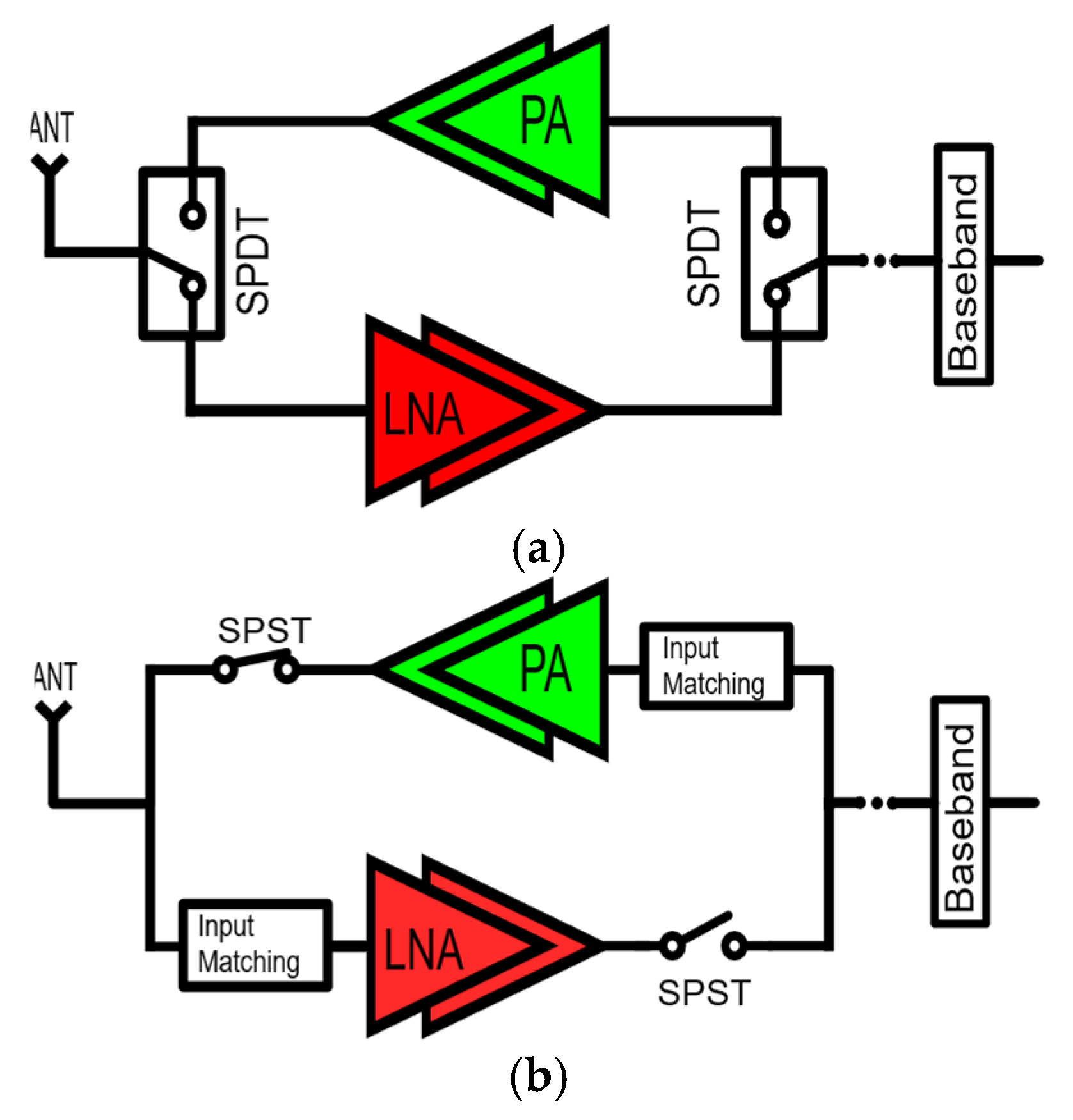
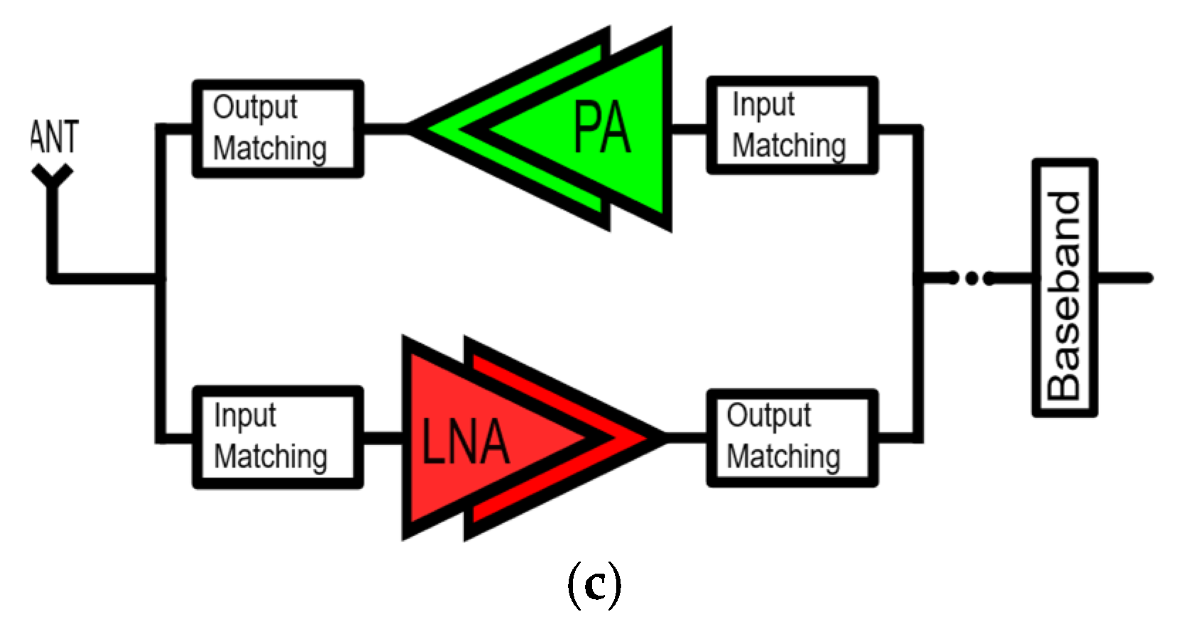
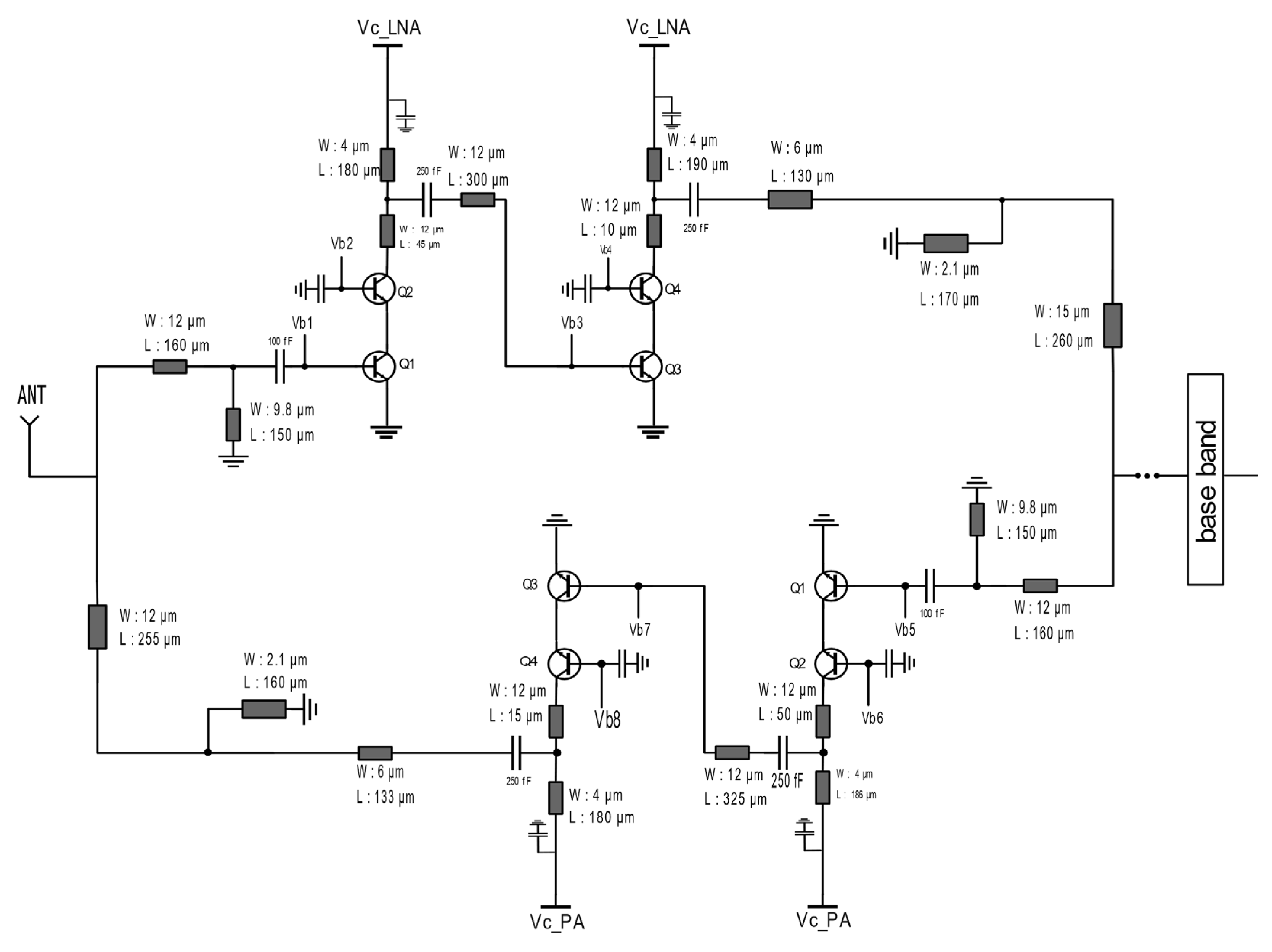
The block diagram of the proposed switchless PALNA architecture is shown in
Figure 1c. Unlike conventional implementations that rely on Single-Pole Double-Throw (SPDT) switches to alternate between transmit and receive paths (
Figure 1a [
7]), or simplified versions that use Single-Pole Single-Throw (SPST) switches to overcome output isolation challenges in each amplification path (
Figure 1b [
8,
9]). This architecture uses a bidirectional configuration where the LNA and PA share a common path, with impedance transformation networks ensuring isolation and proper matching between transmit and receive modes.
To operate in either mode, the biasing is adjusted to make one of these amplifier paths active. In the Tx mode, the transmit path is activated by biasing the PA, while the LNA is switched partially OFF by adjusting its bias and supply voltages, preventing any positive feedback from the receive path. In Rx mode, the receive path is activated, with the LNA turned on and the PA switched partially OFF.
- A.
LNA Design
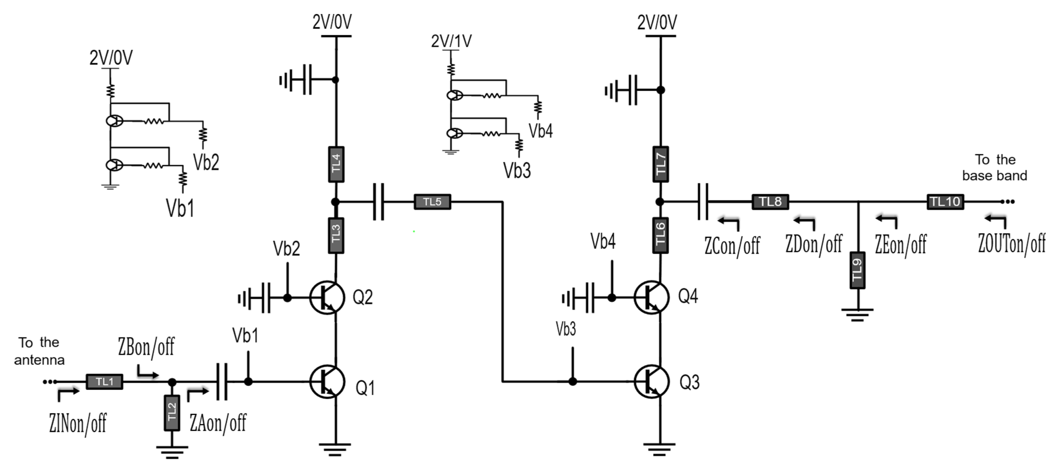
The schematic of the proposed W-band LNA is presented in
Figure 2. It consists of two cascode stages. This topology was chosen because it offers better gain with a low increase in the noise figure compared to the common emitter topology. The LNA is optimized for low-noise performance by properly scaling the transistor dimensions and bias currents. The output of the first stage is directly matched to the input of the second stage to avoid losses.
Since the input of the LNA is shared with the output of the PA, an isolation network is used to provide a high impedance in transmit mode to minimize dissipation losses and to ensure proper matching toward the antenna in receive mode.
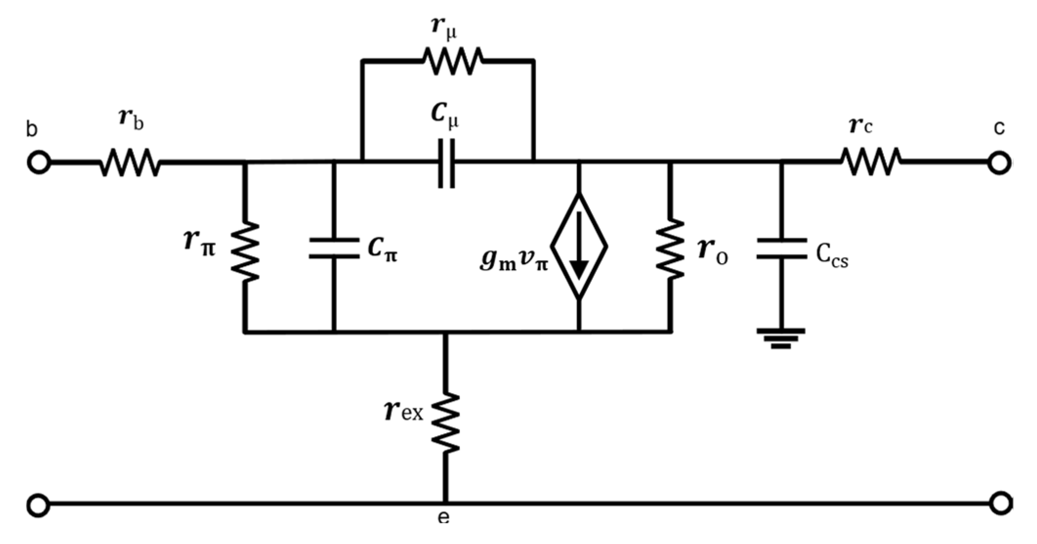
To understand how the isolation behavior depends on the LNA state, a small-signal model of the bipolar transistor is considered. A relatively complete model is presented in
Figure 3, suitable for hand analysis. In general, a hierarchy of small-signal models can be established, ranging from simplified versions to more complex ones typically used in computer-aided design. In this work, a simplified model is adopted to facilitate the analysis and extraction of key parameters.
In this simplified model, the resistance r
μ between the base and the collector is neglected, as high-frequency behavior is mainly dominated by the junction capacitances C
µ and C
π. Among the extrinsic resistances, r
b is the most significant. The other parasitics, such as r
ex, r
c, and the collector-substrate capacitance C
cs, are also neglected to simplify the analysis [
10].
As demonstrated in [
11], the properties of the isolation network change when the LNA bias is switched from an active (or on) state to a cutoff (or off) state. The impedance seen by the isolation network is determined by the transistor parameters of the LNA device (Q1) of
Figure 2. The input impedance of transistor Q1 is determined by its base resistance r
b and the combined effect of the base-emitter capacitance C
π and the Miller capacitance between the base and collector C
µ. These capacitances form a total input capacitance C
t = C
µ + C
π, which varies depending on the bias conditions.
In receive mode, the LNA is biased, and the value of the capacitance C
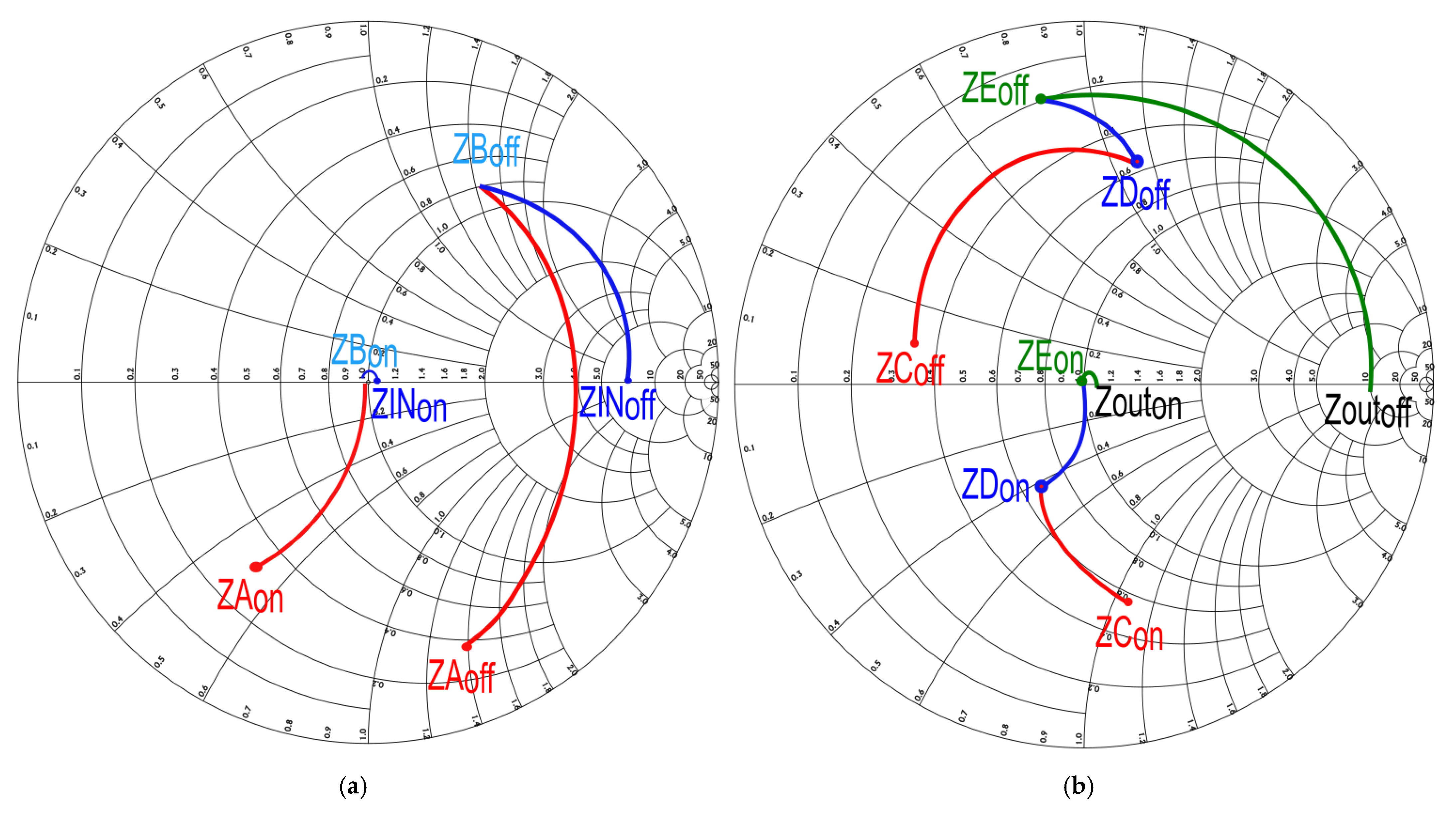
t increases while the Miller effect capacitance depends on the transistor gain. Thus, the input of the LNA presents the impedance ZAon (12 − j* 29 Ω) equivalent to a low resistance in series with a low reactance, as can be seen on the Smith chart in
Figure 4a. This impedance is transformed into 50 Ohms using transmission line TL2. Transmission line TL1, with a characteristic impedance of 50 Ohms, operates when the LNA is deactivated and has minimal impact in active mode.
In transmit mode, the LNA bias is set to 0, and the capacitance Ct is reduced to the base-emitter capacitance Cπ. Therefore, the input of the LNA presents the impedance ZAoff (17 − j* 85 Ω) equivalent to a low resistance in series with a higher reactance. This impedance is then transformed into ZBoff due to TL2 and further transformed into a high-value resistance ZINoff (390 − j* 39 Ω) by TL1, which forces the signal to propagate toward the antenna.
On the output side, the impedance remains nearly constant in both active and inactive states. This limited difference complicates the design of a matching network capable of ensuring, on one hand, proper power transfer or 50 Ω matching when the path is active, and on the other hand, a high impedance—close to an open circuit—when the path is inactive. This behavior is mainly related to the intrinsic properties of the bipolar transistor used in the cascode output stage.
To analyze the output impedance of a cascode configuration, the emitter resistance r
ex, which appears in the common-emitter model shown in
Figure 3, is effectively replaced by the output resistance of the lower transistor in the cascode stack. In this configuration, the total output impedance can be approximated as the parallel combination of the intrinsic output impedance of the cascode stage Z
cascode, and the impedance associated with the Miller capacitance C
μ of the upper transistor.
The collector–base junction of the cascode transistor directly defines the Miller capacitance C
μ, whose value depends on the applied bias conditions. Three regimes can be identified based on the base voltage: equilibrium (no bias), reverse bias, and forward bias. In equilibrium, the depletion region has a fixed width resulting in low C
μ. Under reverse bias (active mode), the depletion region widens, decreasing C
μ. Conversely, forward bias (semi-active mode) reduces the depletion width, significantly increasing C
μ. When the cascode transistor operates in reverse bias (active mode), the depletion region expands, leading to a decrease in capacitance. This capacitance can be modeled by [
12]:
where C
μ0 is the zero-bias capacitance, V
CB is the reverse bias voltage, V
0C is the built-in voltage, and m is the grading coefficient. For the considered transistor model VBIC (Vertical Bipolar Intercompany Model), simulations show that C
μ changes slightly, from 3.83 fF to 3.686 fF, as the transistor switches from the OFF state to the ON state, indicating minimal variation in output impedance between active and inactive states.
In previous PALNA architectures, this limited change necessitated the use of SPST switches to effectively isolate the inactive path. To eliminate these additional components, this work investigates the variation of Cμ in the OFF state under conditions where all other bias voltages are disabled, and only the base voltage Vb of the common-base transistor in the output-stage cascode is applied and varied.
Table 1 shows that for low Vb values (0.2 V to 0.6 V), the capacitance increases slightly, and the collector current remains very low, suggesting weak conduction. However, for Vb = 0.7 V, a rapid increase in both C
μ and collector current is observed, with the capacitance reaching 1.2 pF at 0.9 V and 22 pF at 1 V, while the current rises to 247 µA at 0.9 V and 3.7 mA at 1 V.
This behavior is consistent with the cascode base–collector junction entering forward bias and conducting as a diode, and its conduction grows approximately exponentially with the applied bias:
Since the input transistor (in common-emitter) is left unbiased, its collector–emitter path behaves like a very high impedance and its reverse gain βR is very small. As a result, almost no current flows downward. Instead, most of the base–collector current is directed upward to the cascode collector node, which explains the observed increase in collector current.
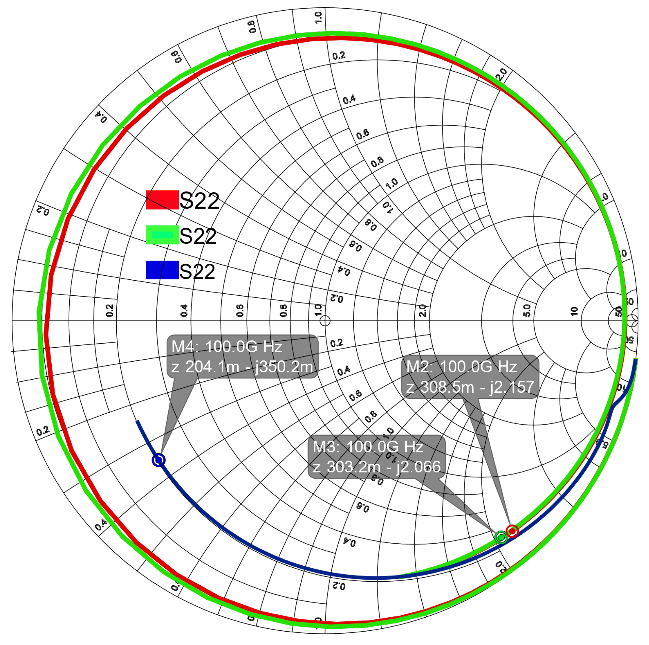
To further illustrate this effect,
Figure 5 presents a comparison of the S22 parameter of the cascode output stage under three operating conditions: (1) active mode, with all bias voltages applied; (2) OFF mode, with all biases removed; and (3) a semi-active mode, where only the base voltage Vb = 0.9 V is applied. In this intermediate configuration, the output impedance becomes predominantly capacitive compared to the other two cases. Based on this behavior, two operating states are selected to simplify the circuit design: the active mode, with full biasing, and the inactive mode, with only Vb applied.
In receive mode, the LNA presents an output impedance ZCon (30 − j* 55 Ω), matched to 50 Ω using a three-line network (TL8–TL10), as shown in
Figure 2. TL8 and TL9 perform the main impedance transformation, while TL10 (50 Ω characteristic impedance) has negligible effect in this mode. The impedance evolution is illustrated on the Smith chart in
Figure 4b.
In transmit mode, the LNA is turned off except for the second-stage current mirror biased at 1 V, in order to maintain approximately 0.9 V at the base of the upper cascode transistor. Which forward-biases the base-collector junction without significant current draw. The resulting output impedance ZCoff (22 + j* 5 Ω) is transformed by the same network into a high impedance, providing effective isolation. In this state, TL10 contributes to converting the impedance seen at the output to approximately 500 Ω (Zout_OFF = 480 − j* 15 Ω), without requiring additional switching elements.
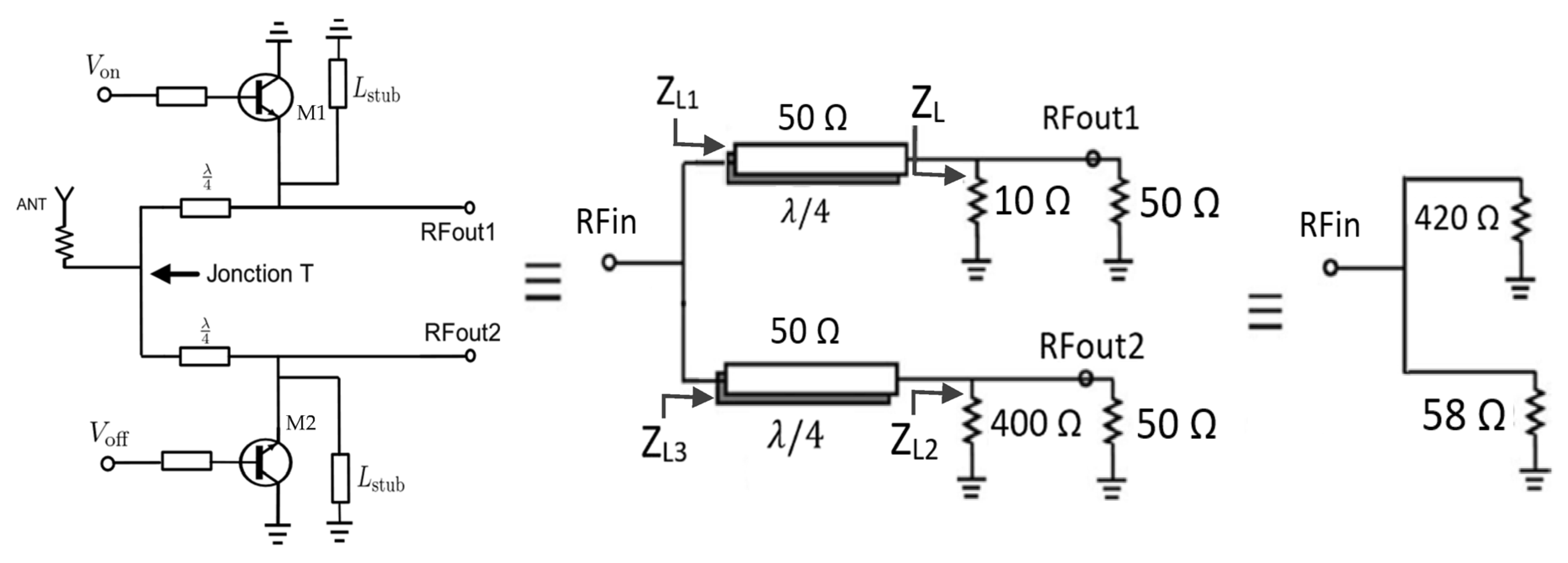
This impedance transformation approach using transmission lines has already been validated in the design of a reverse-saturated Single Pole Single Throw (SPDT) switch fabricated in the same technology and operating in the W-band at a center frequency of 100 GHz. The principle of impedance transformation for this topology is illustrated in
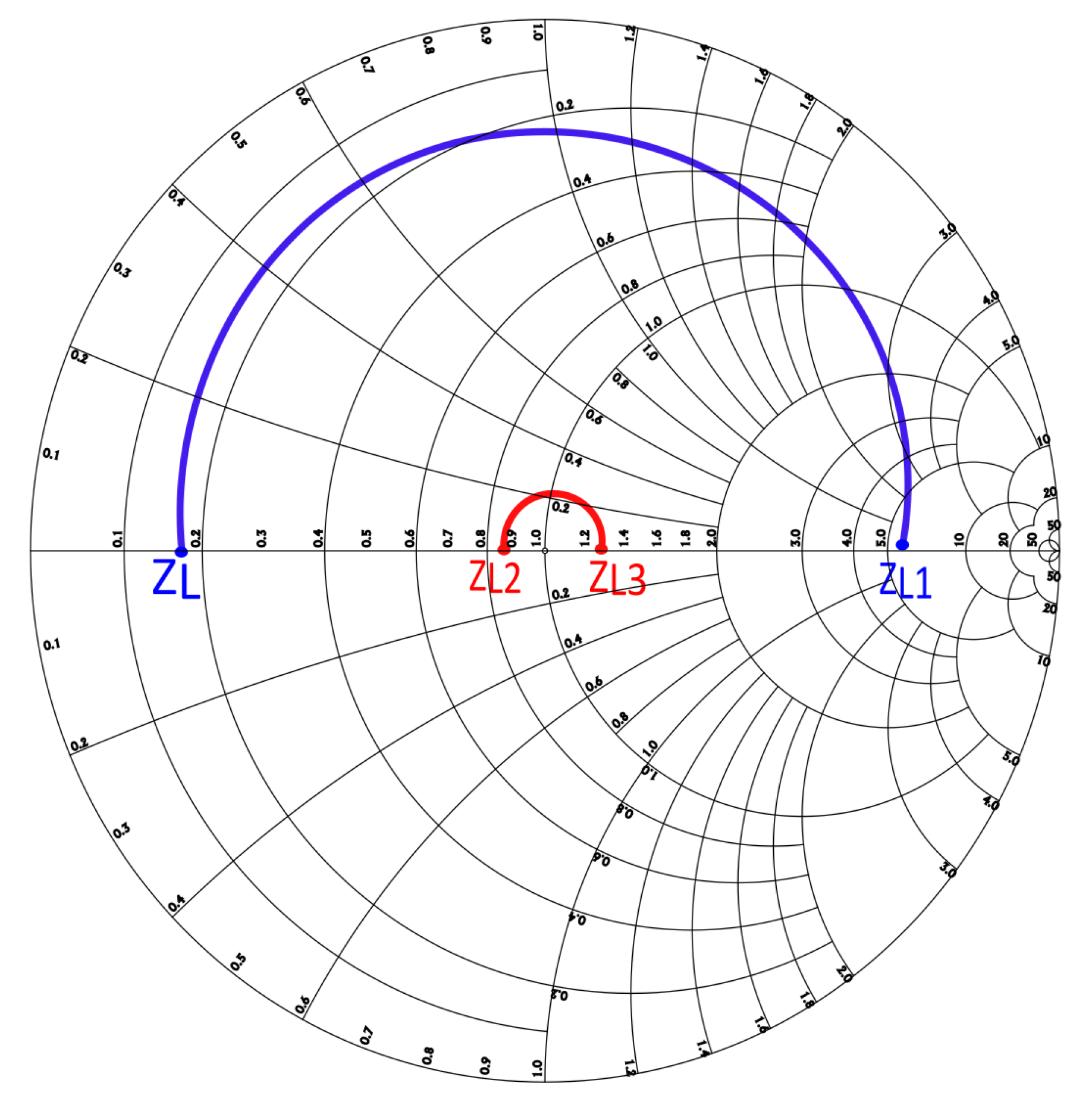
Figure 6 from left to right. When a control signal is applied, transistor M1 is switched ON and presents a low impedance (Ron ≈ 10 Ω) in parallel with the RFout1 node. The λ/4 transmission line, referenced to 50 Ω, then transforms this impedance into a high value (ZL1 ≈ 420 Ω), which is effectively seen as an open circuit, forcing the RF signal to propagate toward the RFout2 path. At this stage, transistor M2 is kept OFF (no control signal applied), and therefore exhibits a high impedance (Roff ≈ 400 Ω). Through the λ/4 line, this impedance is transformed close to 50 Ω (ZL2 ≈ 58 Ω), which allows nearly the entire RF signal to pass to the load. The impedance transformation mechanism, starting from the load impedances and arriving at the transformed impedances Z
L1 and Z
L3 through quarter-wave 50 Ω lines, is further illustrated on the Smith chart in
Figure 7.
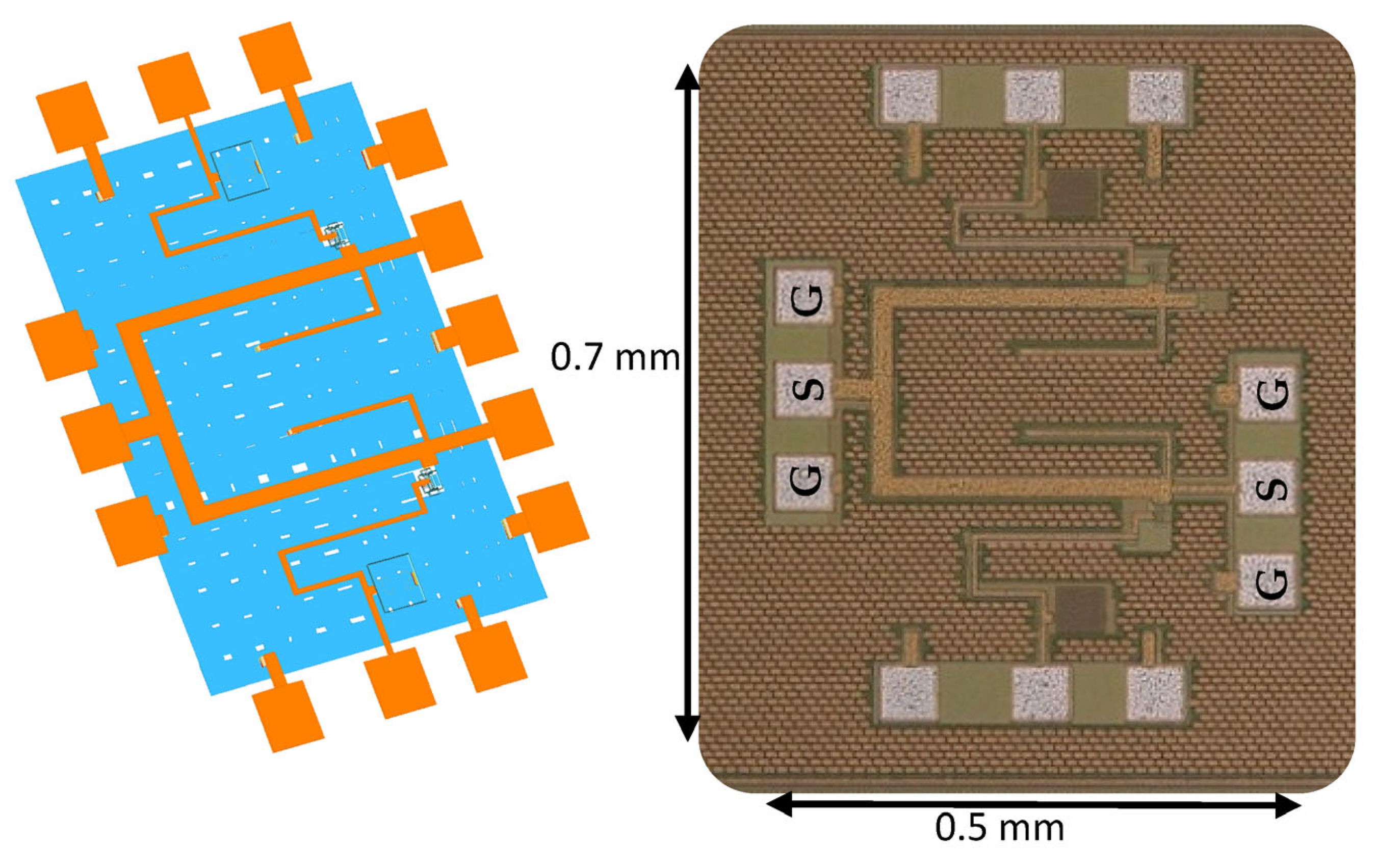
The die photograph of the SPDT switch is shown in
Figure 8. To facilitate two-port measurements, one port on the chip was internally terminated with a 50 Ω resistor. The corresponding measurement results are plotted in
Figure 9, demonstrating excellent agreement with simulations.
Figure 9a compares the measured and simulated S11 parameter in both switching states: when the measured port is biased (active) while the other path is left unbiased, and conversely, when it is unbiased and the other path is active.
Figure 9b shows that the switch achieves an insertion loss of 2.5 dB at 100 GHz with an isolation greater than 16 dB over a 20 GHz bandwidth. These experimental results confirm the effectiveness of the transmission-line impedance transformation technique, further justifying its use in the proposed LNA design.
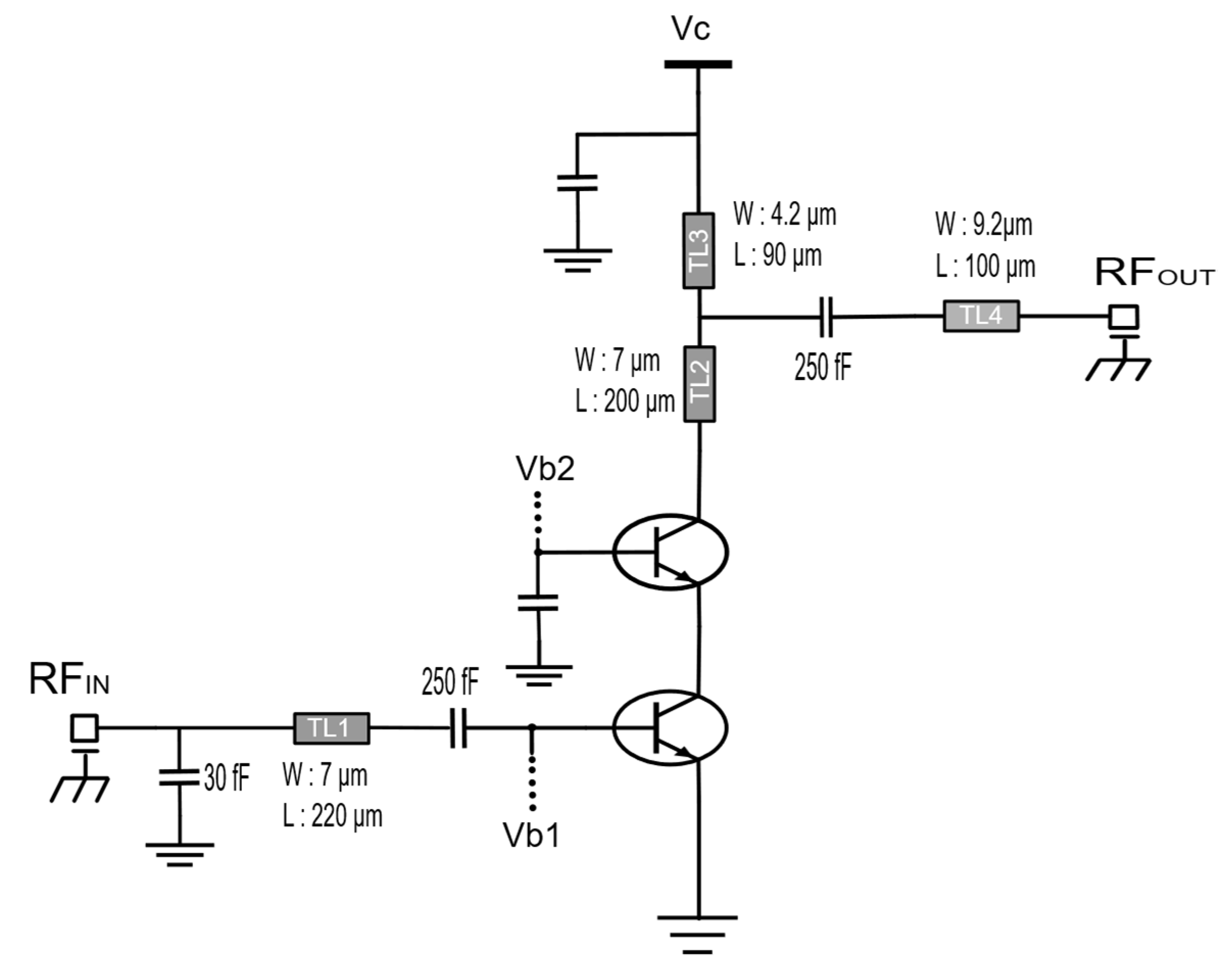
To validate the proposed methodology for the design of a switchless bidirectional PA/LNA targeting W-band frequencies, and, in particular, to demonstrate the effectiveness of the new impedance transformation technique adopted in the switchless architecture, a single-stage cascode LNA (
Figure 10) was fabricated and measured. The circuit draws 5.5 mA from a nominal 1.8 V supply, corresponding to a total power consumption of 10 mW.
To obtain accurate post-layout predictions at W-band, we used a hybrid electromagnetic (EM)/parasitic extraction (PEX)co-simulation flow: selected passive structures and interconnects (e.g., matching networks and transmission lines) were modeled with full-wave electromagnetic simulations (Keysight Momentum, Keysight Technologies, Santa Rosa, CA, USA), a 3D planar (2.5D) EM solver, while the active devices and resistors were back-annotated using parasitic extraction (Cadence PVS QRC, Cadence Design Systems, San Jose, CA, USA). Combining these datasets yields a back-annotated post-layout schematic that captures the circuit behavior with high fidelity and supports the measurements reported here.
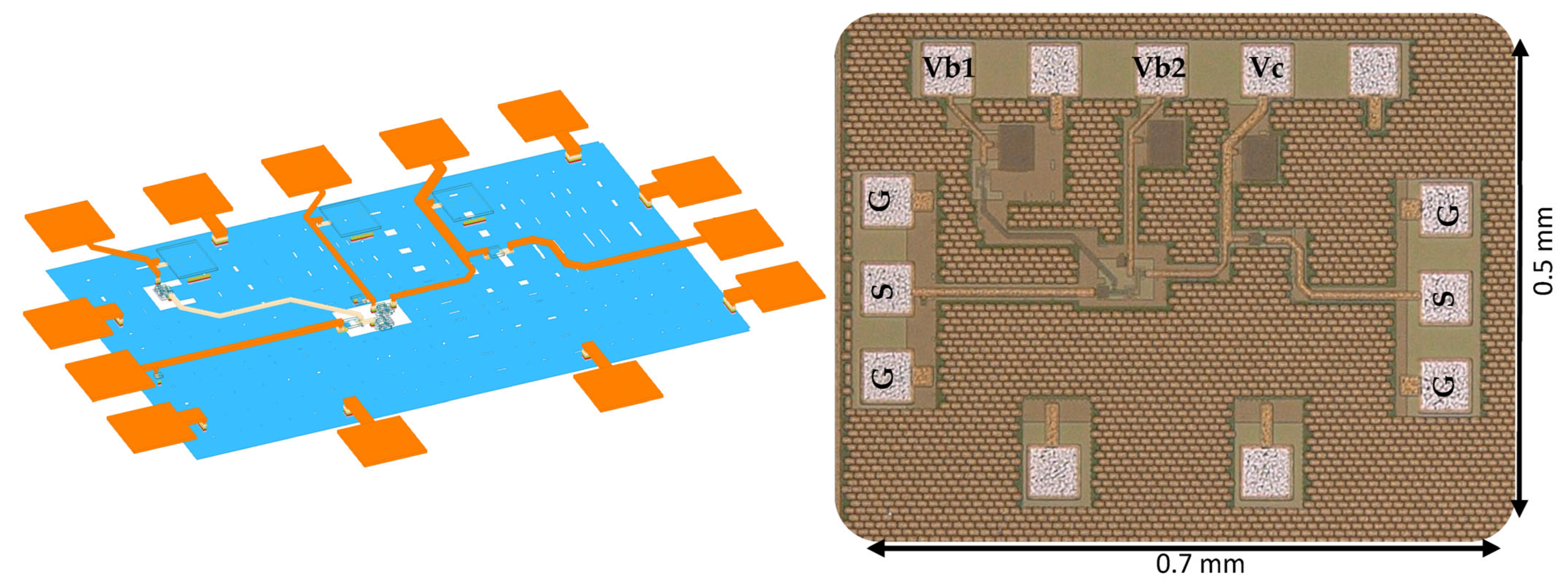
The S-parameters of the fabricated die (
Figure 11) were measured twice. First, at the XLIM research laboratory using a Keysight PNA-X network analyzer (N5247A, Keysight Technologies, Santa Rosa, CA, USA) equipped with W-band frequency extenders (VDI N5262AW10, Virginia Diodes Inc., Charlottesville, VA, USA, 75–110 GHz). The data were then independently re-measured at MC2 Technologies (Villeneuve-d’Ascq, France), a recognized mmWave laboratory, to cross-validate the results.
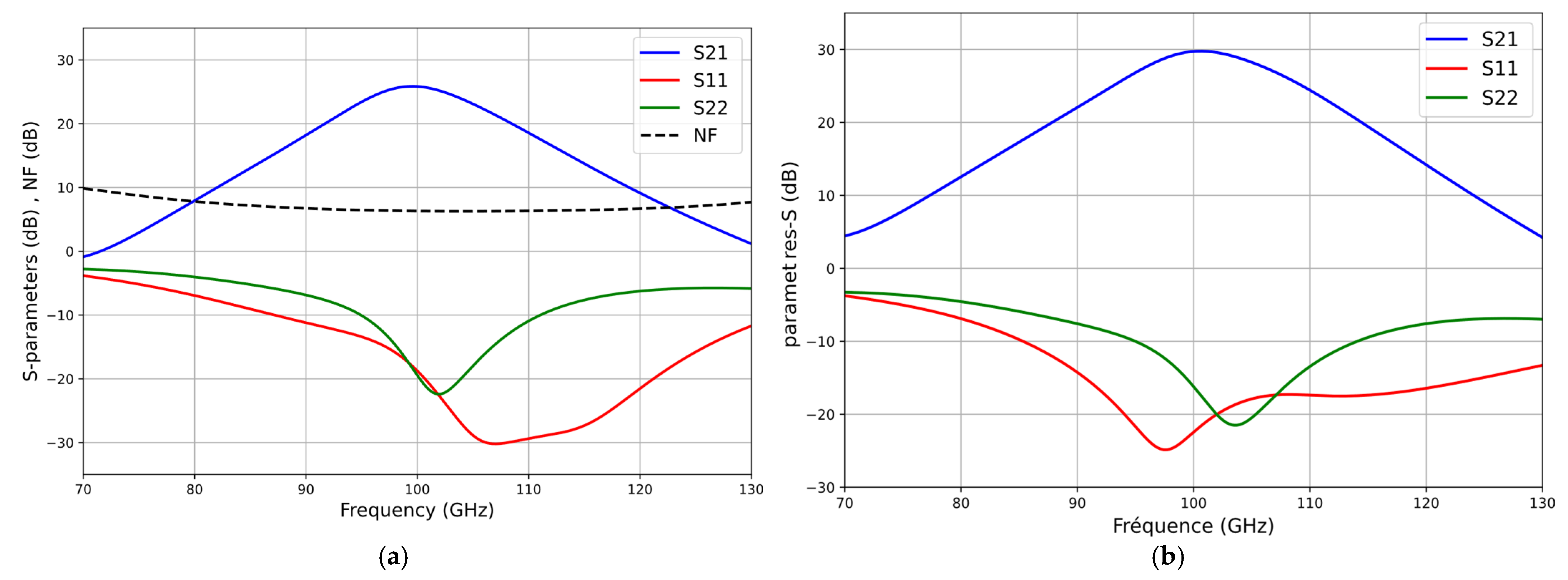
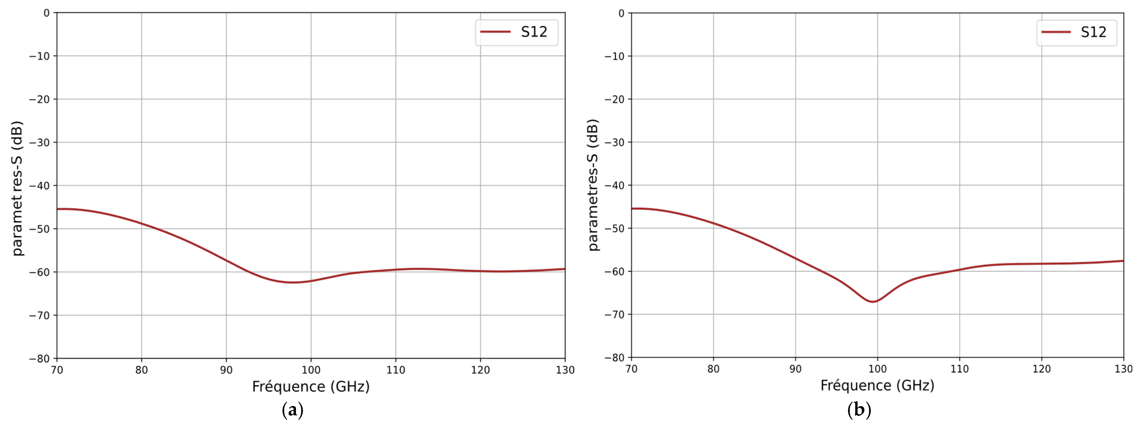
The noise figure was also measured at MC2 using a W-band cold-source method with full vector correction, a setup they use to obtain accurate results up to 110 GHz. The measurement results, including the S-parameters and the noise figure, are presented in
Figure 12. The measured small-signal gain is 16 dB, with a 3 dB bandwidth of 20 GHz, and the noise figure is below 5 dB.
After establishing the measurements, we compared them with post-layout simulations obtained using two EM tools. In addition to Momentum, an independent EM model was generated with EMX.
Figure 13 compares S11 and S22 across the W-band: both tools track the measurements closely, with Momentum showing slightly tighter agreement over frequency. This cross-validation supports the fidelity of the EM/PEX flow used in this work.
Additionally, to validate our theory regarding the variation in the cascode stage output impedance with the bias voltage applied to the base of the upper transistor, measurements were performed on the fabricated LNA, which adopts a cascode topology with three separate bias ports (collector, lower transistor base, and upper transistor base). Accordingly, the output reflection coefficient S
22 was measured under different base bias voltages applied to the upper transistor, as illustrated in
Figure 14.
These measurements confirm that S22 exhibits the same variations observed in simulation, thereby confirming the dependence of the output impedance on the bias applied across the base–collector junction of the upper transistor. The measured power consumption also matches the simulated values. Overall, the results show excellent agreement with simulation, validating the accuracy of the design models, the quality of the circuit implementation, and the robustness of the adopted methodology.
For the design of the PA and LNA that together realize a switchless bidirectional PALNA, we bias the bases of the lower and upper transistors with a cascoded current mirror. Each base is fed through approximately 3.2 kΩ resistors (
Figure 15), which keeps the base current small and, through the voltage drop across these resistors, holds the base node at a low level. As a result, the cascode base–collector junction reaches only a near-forward bias and settles around 0.9 V in the inactive path. This avoids the multi-mA conduction seen at higher bias, keeps Vbc under control across PVT (Process Voltage Temperature) corners and startup transients, and still provides the intended increase in the Miller capacitance C
μ. This was demonstrated over 243 corners using process models typ (typique)/bcs (best case)/wcs (worst-case) for the HBT, resistors, and capacitors;
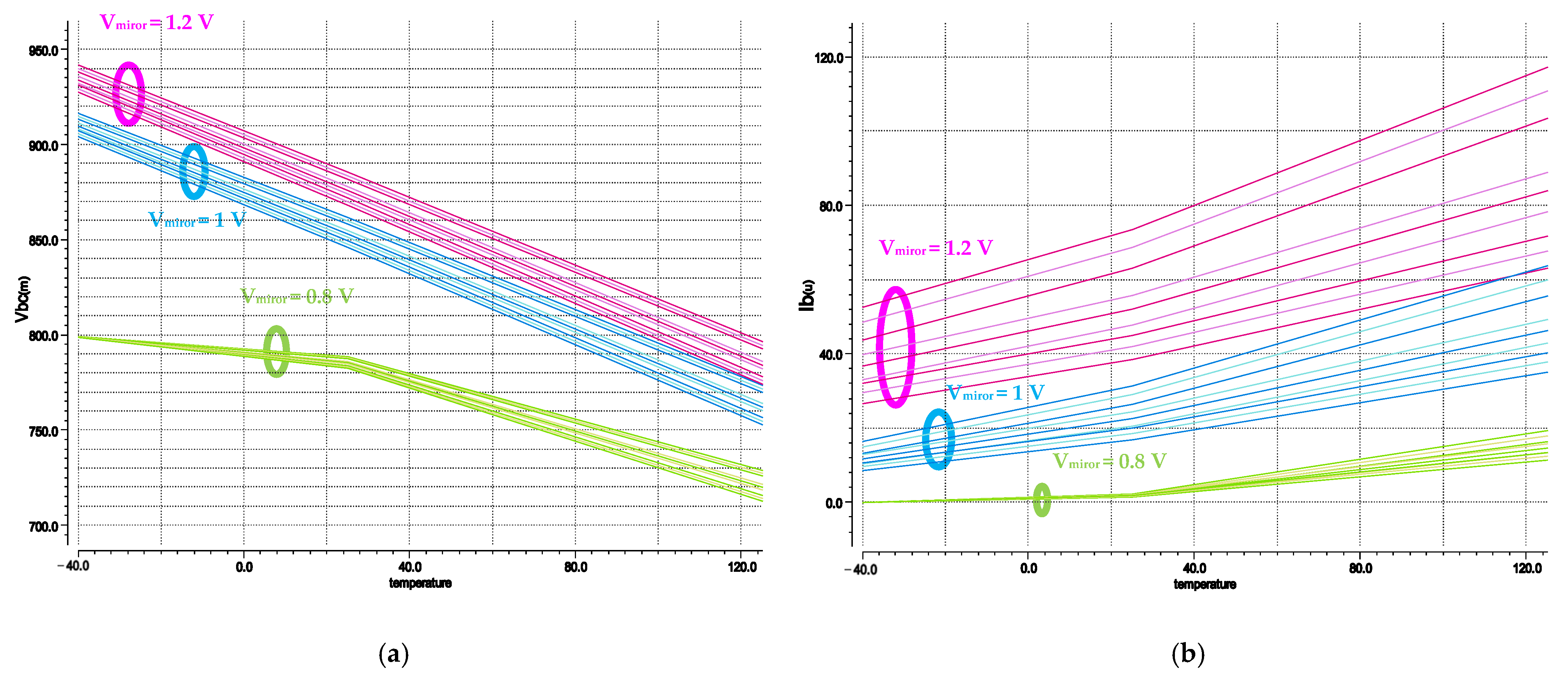
mirror supply and −40/25/125 °C. For each corner we recorded the upper-cascode base–collector voltage Vbc and its base current Ib. In
Figure 16a, Vbc is plotted versus the output voltage across all corners. The curves remain below 1 V in every case, with typical values near 0.9 V, confirming that the cascode junction is only near-forward biased and never enters destructive reverse conduction.
Figure 16b shows the corresponding base current Ib. Even in the worst PVT corners, Ib stays in the few-μA range, demonstrating that the 3.2 kΩ resistors effectively limit the base drive and prevent excess static power dissipation. Together, these results validate the cascode biasing strategy: the design achieves safe Vbc levels, negligible base current overhead, and robust operation across extreme process, voltage, and temperature variations, while maintaining the intended enhancement of C
μ.
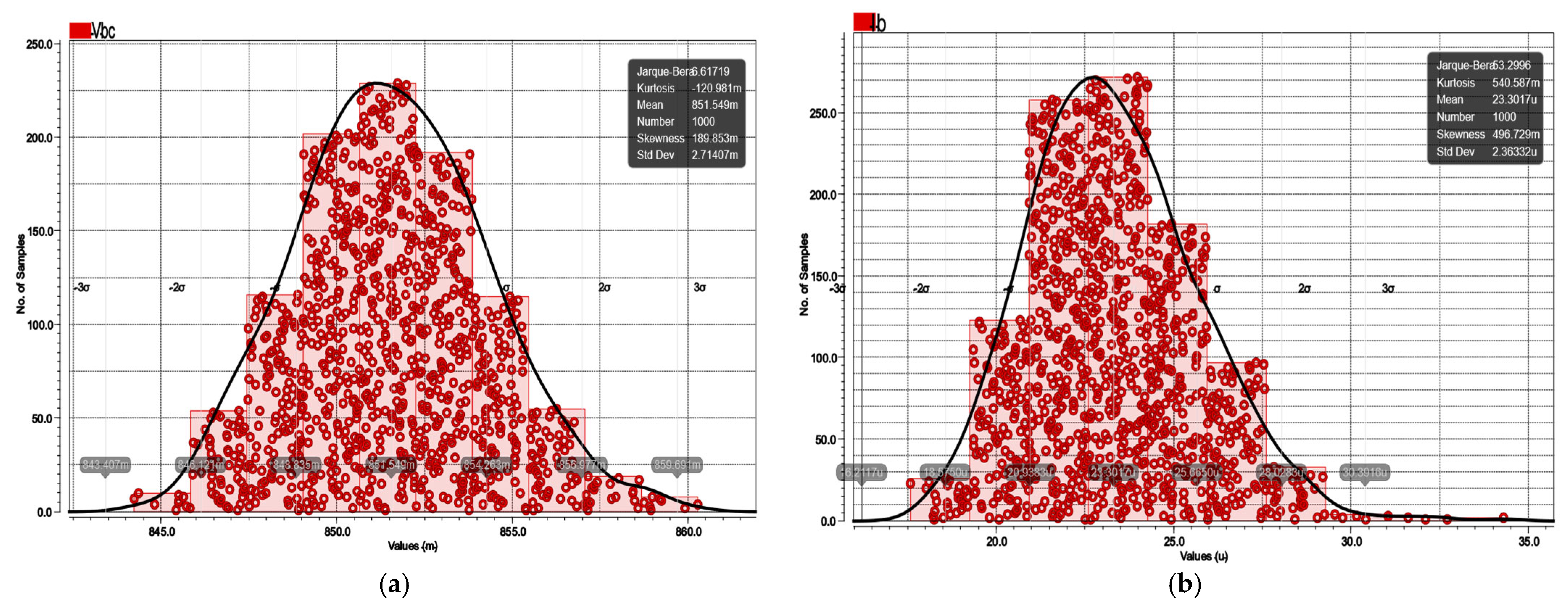
Monte-Carlo analysis was also performed including both process variation and mismatch of the devices and Rbias resistors. The resulting histograms of Vbc and Ib (
Figure 17a,b) are narrow and centered close to their nominal values. For Vbc, the distribution remains clustered well below 1 V, while the Ib distribution shows all samples confined to a few microamperes. These results confirm that even under random mismatch, the inactive-path bias point is well controlled, further supporting the robustness of the cascode biasing approach.
- B.
PADesign
The RX amplifier has the same two-stage cascode topology as the LNA but with different biasing conditions. The first stage shares the same transistor size as the LNA to ensure good isolation between the transmit and receive paths. However, it differs in terms of bias voltage and current density. The second stage is designed to achieve higher output power by employing the load-pull technique to determine the optimal load impedance.
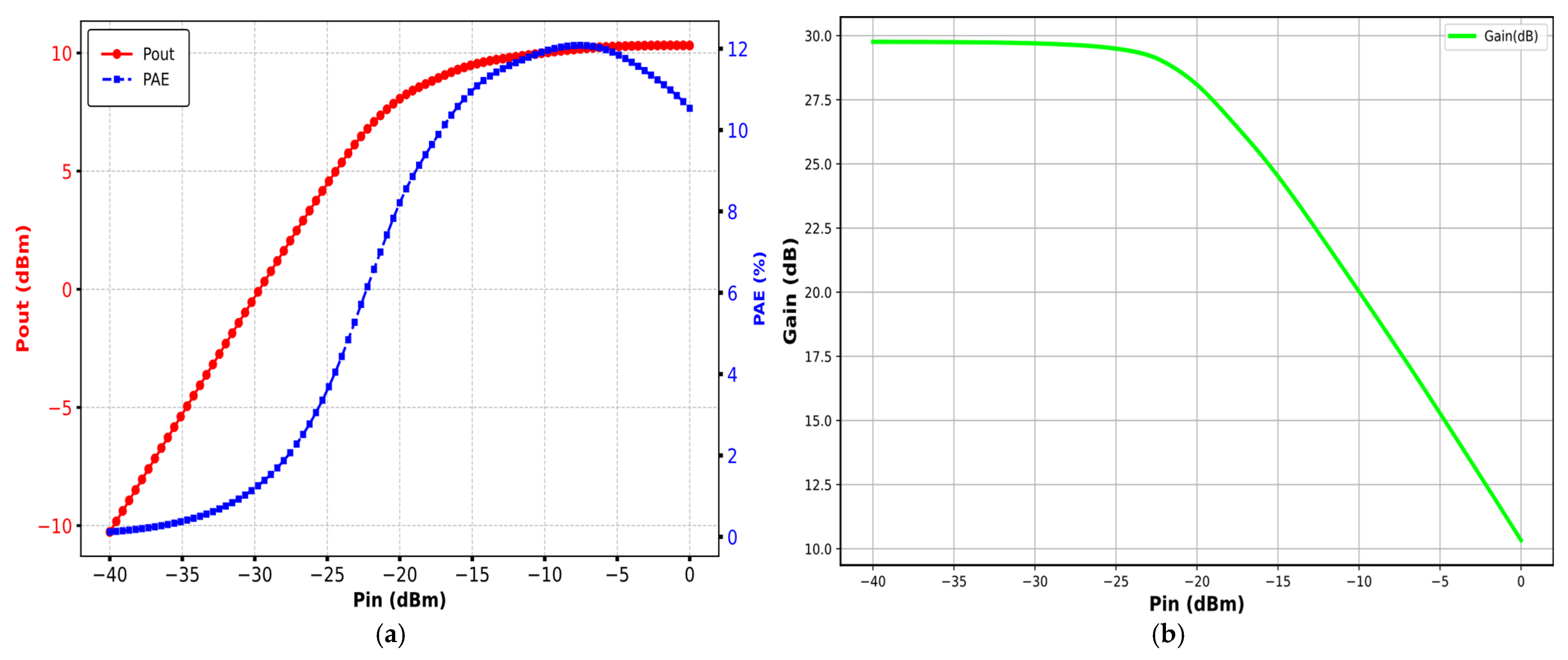
The key differences in the design of the Tx path lie in the biasing parameters and current density, and their impact on the design of the matching networks.
