Article

Common-Mode Noise Estimation for a Boost Converter with Substitution Theorem

1
College of Biomedical Engineering and Instrument Science, Zhejiang University, Hangzhou 310027, China
2
Academy of China Changfeng ELectro-Mechanical Technology, Beijing 100854, China
3
School of Aeronautics and Astronautics, Zhejiang University, Hangzhou 310027, China
*
Author to whom correspondence should be addressed.
Electronics 2025, 14(17), 3375; https://doi.org/10.3390/electronics14173375
Submission received: 29 July 2025 / Revised: 18 August 2025 / Accepted: 20 August 2025 / Published: 25 August 2025
(This article belongs to the Section Power Electronics)

Abstract

With the increasing switching frequencies and power densities in modern power converters, the prediction and mitigation of common-mode (CM) noise are becoming increasingly essential. Even though powerful, simulation methods are hindered by the difficulties in modeling power semiconductors and the long simulation time. As an alternative, the measurement-based substitution model is demonstrated in the paper, which simplifies the non-linear converter with a linear circuit network with multiple independent sources. Transfer functions are then defined and characterized to evaluate the conversion ratio from different sources to the CM noise produced on the attached cables. Good agreements are observed between the predicted and measured CM noise under several test conditions. Additionally, the proposed method facilitates dominant noise source identification and the corresponding noise suppression. The proposed method offers advantages over the existing approach, including simplicity in the characterization of transfer functions and the least disturbance to the test setup.

1. Introduction

DC-DC power converters [1,2,3,4,5] are widely used modules in fields such as consumer electronics and automotive electronics. Strong noise can be observed at frequencies of up to hundreds of MHz due to their fast switching nature, resulting in intolerable interference. With the evolution of wide bandgap devices, switching frequencies have been pushed higher, and more severe electromagnetic compatibility problems have arisen [3,4,6]. To predict and optimize the common-mode (CM) noise generated by power converters, extensive studies have been performed using methods such as hybrid modeling, terminal modeling, and substitution modeling.
Co-simulations of full-wave structures and circuit-level components are utilized in the hybrid modeling method [7,8,9,10]. This technique can be used to analyze the complex interactive behaviors between different structures and components, e.g., the response of the package structure of an IGBT module to CM noise [8]. Although this method provides flexibility for investigating the influence of each component, the method is extremely computationally expensive, requiring a duration of weeks for a single simulation case. In addition, accurate circuit models for semiconductor devices are typically not available. In common practice, SPICE-like behavior models are used to describe the electrical characteristics of MOSFETs or diodes, which limits the usable range of the model to tens of MHz or even lower [9,10].
To bypass these challenges in modeling semiconductor devices, measurement-based methods have been developed for CM noise estimation in different scenarios. Terminal modeling [2,11,12], i.e., in which the equivalent Thevenin or Norton circuit is extracted for a device-under-test (DUT), has been successfully applied to estimate CM noise. We note that the model is effective for analyzing the influences of components loaded to the equivalent source; moreover, a knowledge of the topology and components is not required due to the simplification employed in this model. For instance, the model can facilitate cable routing optimization in a vehicle platform [13]. Correspondingly, optimization of the converter itself is not possible with the method. In addition, the usability of the extracted source can also be locked to a certain configuration, e.g., the parasitic capacitance between the metal ground plane and the DUT is also included in the source impedance.
The substitution method is another technique for overcoming difficulties in modeling non-linear devices [3,4,14,15]. Each non-linear device in a DC-DC converter is replaced by an independent voltage or current source, which is obtained from time-domain measurements, and the linear superposition theorem is applied to evaluate the total noise generated by different components. Compared with the terminal modeling method, the substitution method provides the unique capability to identify the noise contributed by different components. Moreover, the substitution method has been integrated into the terminal modeling method and successfully applied to predict the radiated noise generated by a buck-boost converter [15]. A two-step parameter extraction flow calculates the transfer function between voltage/current sources and the common-mode (CM) current driving unintentional antenna structures (i.e., input/output cables). While this simulation-based approach proves valuable for design-stage noise characterization and mitigation, it generally requires significant time and computational resources, posing practical challenges for time-critical EMI troubleshooting in product development cycles. A purely measurement-based method remains essential for EMI filter optimization to meet stringent product release timelines. Furthermore, the CM impedance measurement procedures necessitate the physical disconnection of input and output cables from the power converter. This intervention introduces significant measurement uncertainty, as minor perturbations to cable positioning, routing, or geometry substantially alter their equivalent radiation impedances. An additional challenge arises in the selection of appropriate source models for nonlinear device substitution. Although theoretical frameworks permit representation using either voltage or current sources, practical implementation lacks consensus on the optimal source type for substitution in real-world applications.
This paper proposes a purely measurement-based methodology for common-mode (CM) current noise estimation in power electronic converters. The primary contribution is a fast one-step measurement technique that directly characterizes the noise transfer function while preserving the integrity of input/output cabling, thereby eliminating the measurement-induced disturbances inherent in conventional approaches. In addition, the methodology enables dominant noise source identification without requiring prior knowledge of noise generation mechanisms, significantly enhancing diagnostic efficiency. Furthermore, the source selection for semiconductor device substitutions in real practice is discussed. The proposed method is experimentally validated on a boost converter.

2. Substitution Model for Boost Converters and the Measurement-Based Noise Estimation Methodology

In this paper, we primarily focus on estimating the output signal of an RF current probe while it is clamped on the output cable of the whole system. The CM noise estimation method is then presented with the substitution model and linear superposition theorem. The boost converter is substituted by a linear circuit network of three independent sources with parasitic impedances of the printed circuit board (PCB) and input and output cables. A one-step transfer function measurement and calculation methods are demonstrated without disturbing the cables of the converter.

2.1. Substitution Model

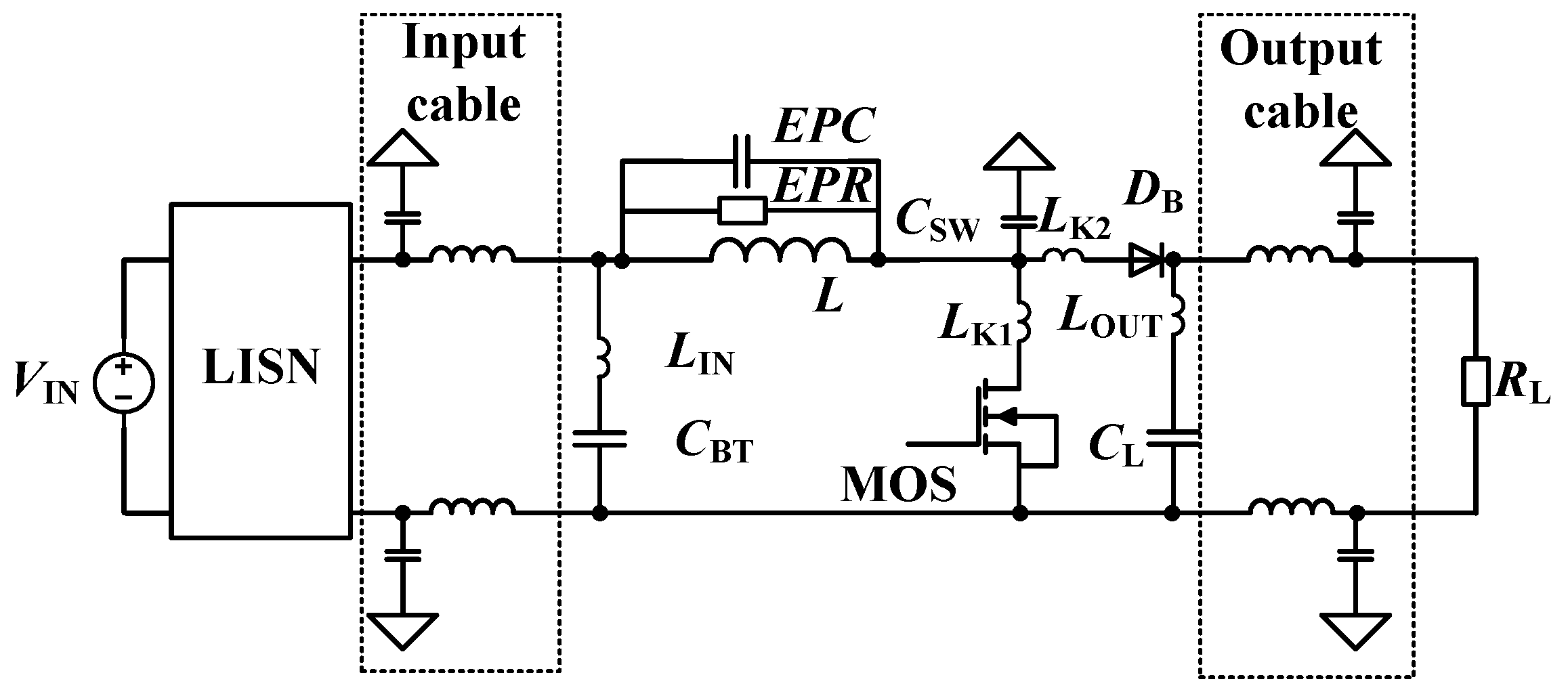
To demonstrate the substitution method for CM noise estimation, an open-loop boost converter is deployed, and the measurement setup is depicted in Figure 1. Input and output cables connect the power converter to a line impedance stabilization network (LISN) and a resistive load R L . Figure 2 illustrates the equivalent circuit model of the boost converter. The LISN is modeled as two 50- Ω resistors, while the cables are represented by equivalent LC circuits. The boost inductor’s parasitic winding capacitance and losses are characterized by an equivalent parallel capacitance (EPC) and an equivalent parallel resistance (EPR), respectively. C B T and C L represents the input and output capacitors of the converter. Furthermore, the model incorporates parasitic elements from components and printed circuit board (PCB) traces, with L I N , L K 1 , L K 2 , and L O U T denoting the equivalent series inductances (ESL) of the PCB, capacitors, diode, and MOSFET, respectively. C S W is the parasitic capacitance between the earth ground and the switching node of the PCB.
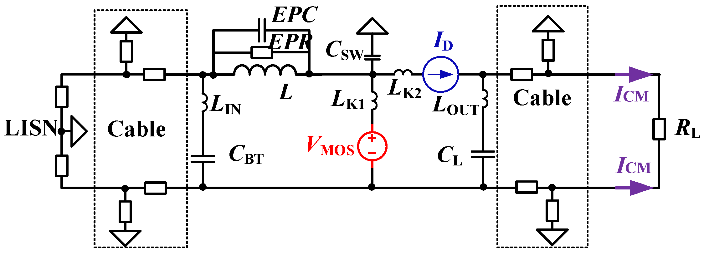
The substitution model has been developed to facilitate the analysis of EMI issues. As the name suggests, a substitution theorem is used to replace one element of the circuit with another element, e.g., an ideal voltage or current source. The semiconductor components can then be replaced by measured waveforms: the MOSFET is typically replaced by a voltage source V M O S , and the diode has been represented by its current waveforms I D in previous practice. When the elements are replaced, the branch currents and node voltages of the whole circuit should remain the same. Therefore, the input capacitor of the circuit should also be substituted with a voltage source. A substitution model for a boost converter is presented in Figure 3 [14].

2.2. Measurement-Based CM Current Estimation Methodology

2.2.1. Noise Estimation Method for the Boost Converter

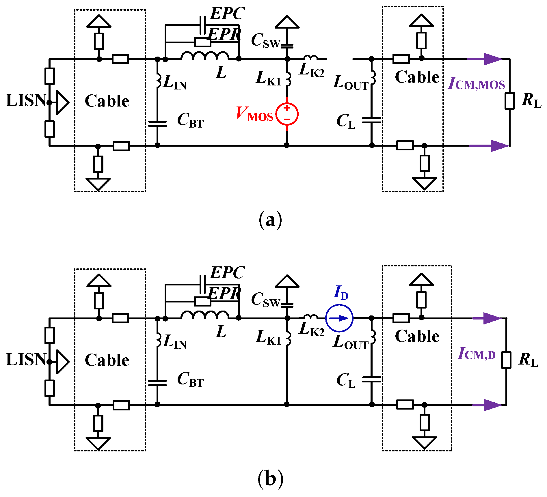
This substitution does not alter the circuit behavior. Notably, the original boost converter containing nonlinear CM current I CM induced at the output cable can then be calculated using the principle of linear superposition of these two independent sources. As illustrated in Figure 4, the simplified equivalent circuit is presented to separately evaluate the contributions from V MOS (MOSFET switching voltage) and I D (diode conduction current). The CM current generated by the MOSFET and the diode can be formulated as follows:
I C M , M O S = V M O S × T F M O S ,
I C M , D = V M O S × T F D ,
where the I C M , M O S and I C M , D are generated by the MOSFET and the diode, respectively. The transfer functions T F M O S and T F D represent the ratio between the output CM current and the amplitude of the sources, as listed below. The amplitudes of the sources can be measured by an oscilloscope and the measurement method for transfer functions will be discussed in the following section.

2.2.2. One-Step Measurement Method for the Noise Transfer Functions

As we have mentioned in the introduction, the input and output cables are required to be removed from the power converter for impedance measurements in the existing method [15]. The proposed one-step measurement approach does not require the detachment of the cables, which minimizes the disturbance. Considering the equivalent circuits in Figure 3 and the measurement setup in Figure 1, the transfer function can be characterized by a VNA, and the MOSFET to the current probe is shown as an example. The superposition theorem should be followed when the MOSFET contribution is evaluated, i.e., other voltage sources should be shorted and other current sources should be disconnected. The measurement setup is illustrated in Figure 5. The transfer function is defined as the ratio between the output voltage V O U T and the input voltage V I N or current I I N . We emphasize that the measured S-parameters should be transformed to Z-parameters, which can remove the influence of the 50 Ω impedance from the VNA. The equivalent circuits for a voltage source-driven case are depicted in Figure 6.
T F V is defined as the ratio between the output voltage V O U T and the ideal input voltage source V I N :
T F V = V O U T V I N .
After the Z-parameters are obtained from the S-parameters [16], the transfer function T F V can then be represented as follows:
T F V = 50 Z P · Z 21 / / Z P Z 21 / / Z P + Z 11 Z 21 = 50 Z 21 ( 50 + Z 22 ) Z 11 Z 21 2 ,
where Z P is defined as follows:
Z P = Z 22 Z 21 + 50 .
Similarly, the current transfer T F I can be formulated as follows [17]:
T F I = 50 Z 21 50 + Z 22 .
We note that the calculation methods can also be used for other test conditions, e.g., to estimate the noise measured by an antenna when it is connected to a 50- Ω measurement instrument.
The boost converter contains two non-linear switching devices, which require substitutions for two sources. The method can be further extended for an arbitrary power converter with multiple non-linear switching devices. A flowchart for CM noise estimation is presented in Figure 7. The waveforms of semiconductors in the converter should be measured and transformed to the frequency domain. We assume that M voltage sources and N current sources are obtained in the substitution model. The amplitude and phase of the ith voltage or the jth current source can be calculated through FFT:
| V i t h | e j ϕ V i t h = F F T ( V i t h ) ,
| I j t h | e j ϕ I j t h = F F T ( I j t h ) .
The total CM noise can then be calculated by the following:
V T o t a l = i = 1 M V M × T F V M + j = 1 N I N × T F I N .
The total CM noise produced by the converter is the summation of the noises generated by the MOSFET and the diode. It should be emphasized that the waveforms are recorded in the time domain by an oscilloscope and converted to the frequency domain by a fast Fourier transform (FFT).

2.3. Considerations in Real Practice

2.3.1. Substitution Model with Current Sources

In theory, the effectiveness of the substitution method is not influenced by the source type, i.e., enforcing current or voltage information. However, current measurements at frequencies of dozens or even hundreds of MHz are challenging. Resistive current sensors have been typically used in previous studies [3,4] applying Ohm’s law for a direct current-to-voltage conversion. Nevertheless, the equivalent series inductance (ESL) of an ordinary two-terminal resistor is typically in the nH range and can introduce large errors. For instance, the impedance of a 1-nH ESL is as large as 0.6 Ω at 100 MHz, and the resistance should be configured as at least 6 Ω to guarantee the validity of the current measurement. The loading effects of this large resistor can greatly disturb the operation of the converter, and thus, current sensing with a discrete chip resistor is not feasible. The current can also be measured by a current transformer, a coaxial current-viewing resistor, or a Rogowski coil, but these devices have limitations regarding difficulties in installation or operation bandwidth [17]. To summarize, substitution with current sources should be avoided in real applications due to difficulties in current measurement.
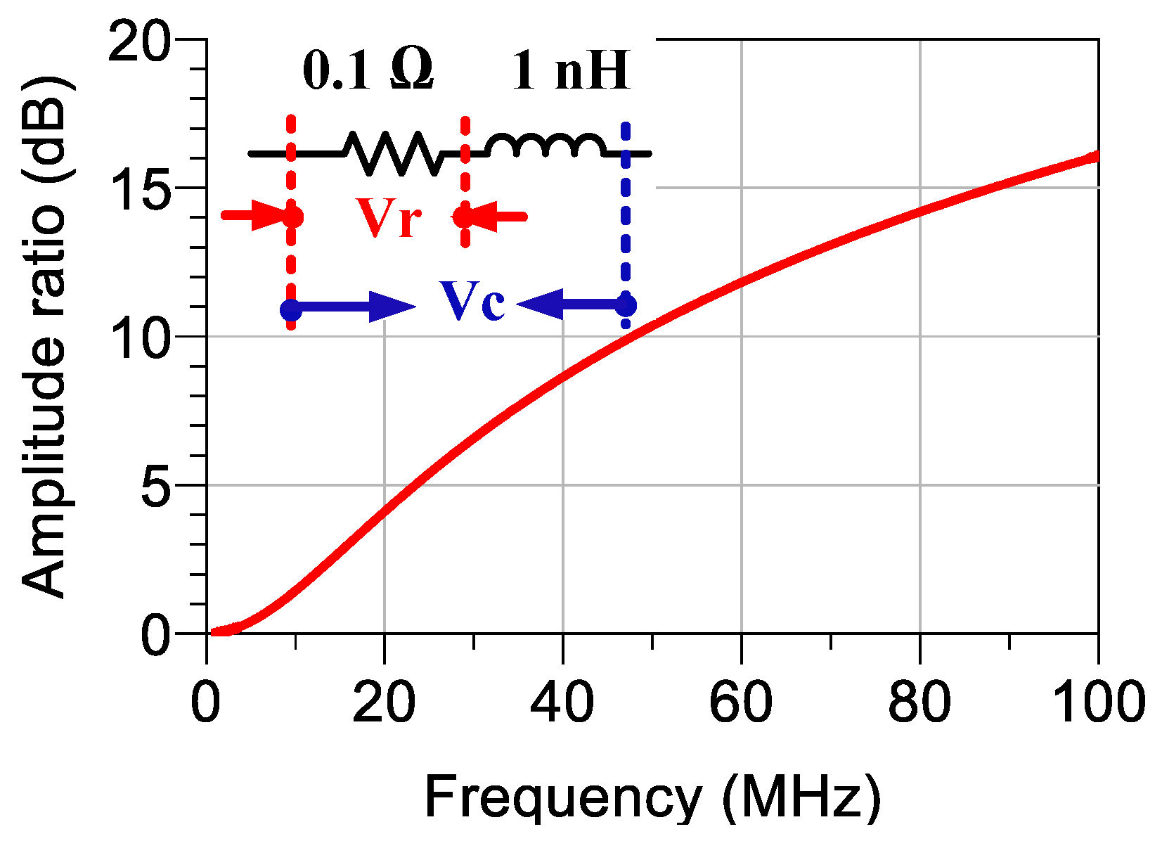
A simulation case was considered to compare the current measured by a sensing resistor (0.1 Ω ) with and without the ESL (1 nH), as plotted in Figure 8. The amplitude ratio A R is defined as the voltage induced across the resistor and the RL circuit for different values of the excitation frequency f:
A R = V c V r = R + j 2 π f L R .
The usable range of a current sensing resistor is limited to ∼15 MHz (considering a 3-dB bandwidth), and the current measured by a current sensing resistor can be significantly overestimated for frequencies of tens of MHz. The unknown phase shift of the resistor is another concern, as phase information is also important during the superposition process.
Fortunately, the loads of the boost converter, including the cables and resistor, are linear components. The node voltages and branch currents remain the same when the diode is substituted with a voltage source, as illustrated in Figure 9. Moreover, the measurements for voltage waveforms can be performed with the same differential voltage probe, which increases the consistency in the source characterization.

2.3.2. Considerations for Transfer Function Measurements

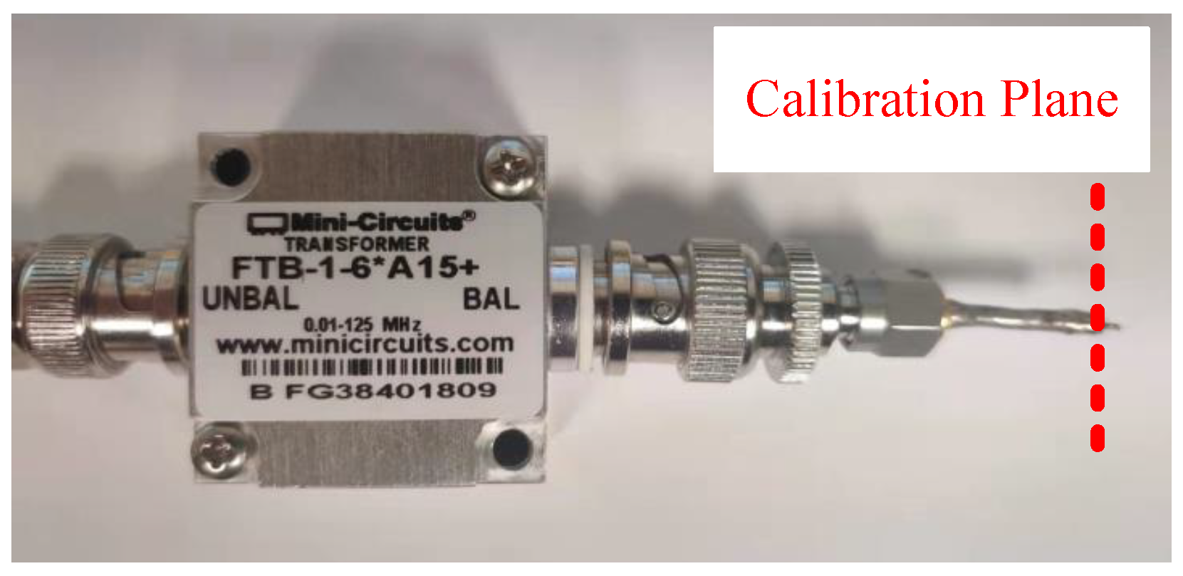
The transfer function can be used to effectively evaluate the conversion from a single source to the CM noise of the whole board. However, unwanted loading effects, except for the port impedance of the VNA, should be minimized. The CM impedance between the PCB and the measurement instruments, from both the VNA and the attached cables, can be rejected by adding ferrite beads and balun. As shown in Figure 5, two common chokes (model: WE 74275812, 200 Ω @ 100 MHz) were added to each cable. In addition, a balun (model: Mini-Circuits, FTB-1-6*A15+, 10 kHz–125 MHz) and a 2 cm semi-rigid cable were used in the measurement, as displayed in Figure 10.
As shown in Figure 11, the measurement configuration and corresponding S21 responses under reversed polarization states of Port 1 demonstrate consistent agreement, with observed discrepancies remaining below 3 dB across the operational bandwidth. This further validates the measurement method for the noise transfer function.

3. Experimental Verification

This section presents experiments performed in a semi-anechoic chamber to demonstrate the accuracy of the proposed method. In addition, the proposed method can be applied to identify the dominant noise source in a converter. Last but not least, the CM noise mitigation methods can be strategically applied according to the dominant source analysis.

3.1. Measurement Setup

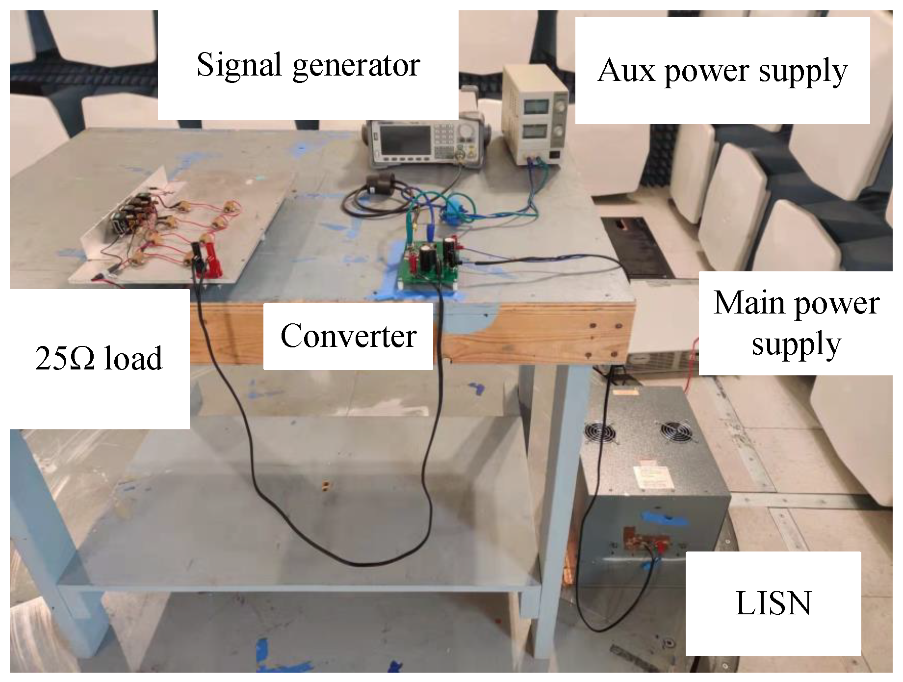
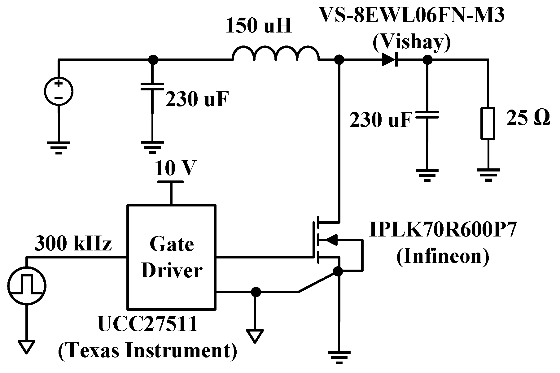
The configuration of the measurement setup is shown in Figure 12, where the frequency range of interest is 30–125 MHz (limited by the bandwidth of the balun). The setup consists of the main power supply (TDK-Lambda GEN 500-10), a LISN (FCC-LISN-50/250-25-2), and a boost converter board. The waveforms of the noise sources are measured by a differential voltage probe (Tektronix 6251, with a 1103 power supply), and the CM noise is evaluated by an RF current probe (FCC-F65). An oscilloscope (R&S RTO1024) and a VNA (Agilent E5071C) was used for time- and frequency-domain measurements, respectively. The sampling rate of the oscilloscope was set to 1 Gs/s, and the resolution bandwidth of the FFT was 1 kHz. The circuit diagram and the components used in the board are labeled in Figure 13.
The boost converter was designed with an open-loop configuration and is controlled by an external signal generator (Siglent SDG2042x). To avoid unintentional noise introduced by the gate driving circuits, ferrite rings were also added.

3.2. Comparison of Measured and Calculated Noise

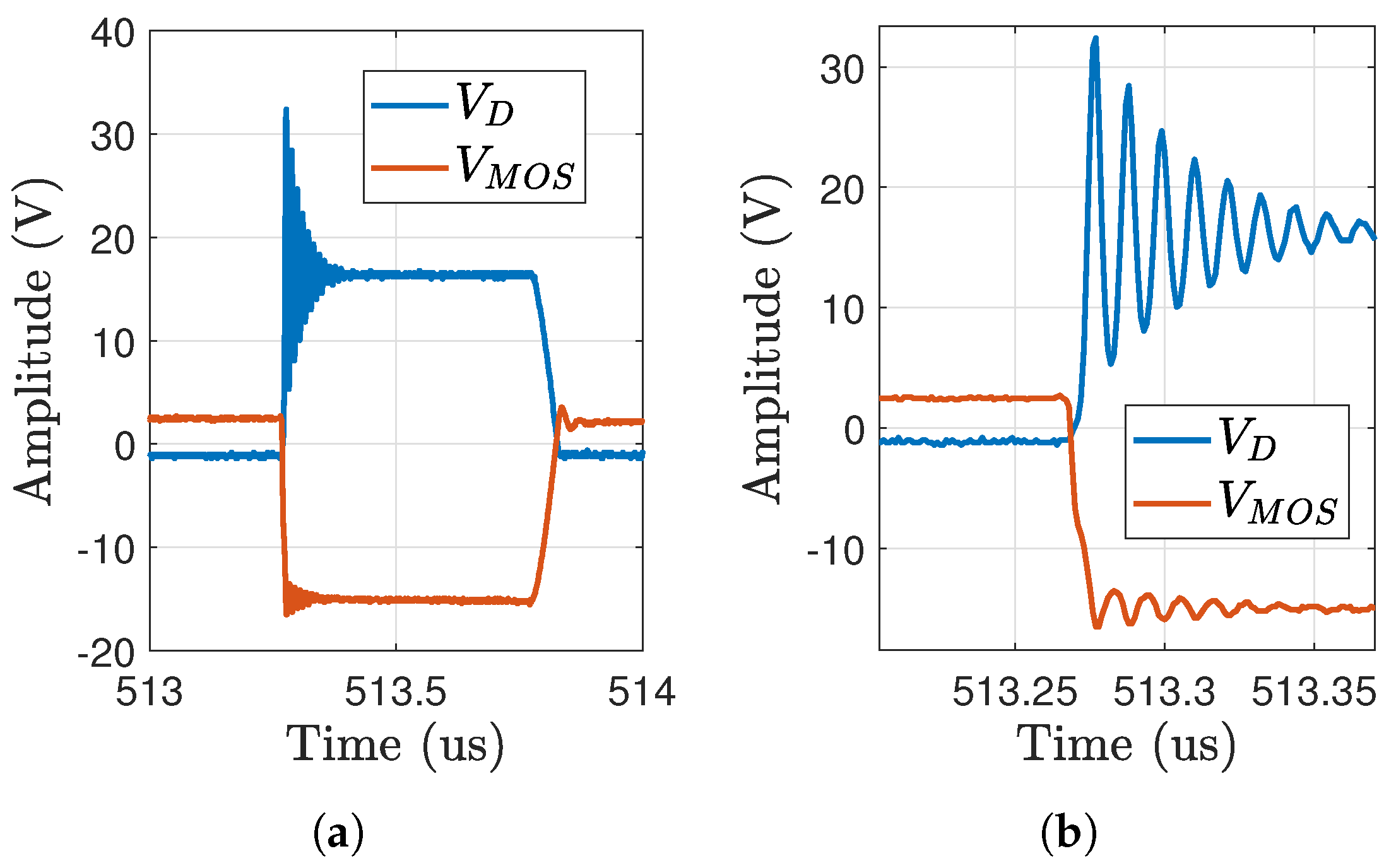
In the proposed methodology, the CM noise measured by the current probe is calculated by the total contribution of different sources. We note that both amplitude and phase information are required in the calculation, and the drain-to-source voltage of the MOSFET and the voltage across the diode are measured with an oscilloscope, as shown in Figure 14. The DC rejection of the probe is enabled to make full use of the dynamic range of the probe. It can be seen that strong ringings occur during the turn-on transition of the MOSFET, and the noise generated across the diode is much higher than that of the MOSFET.
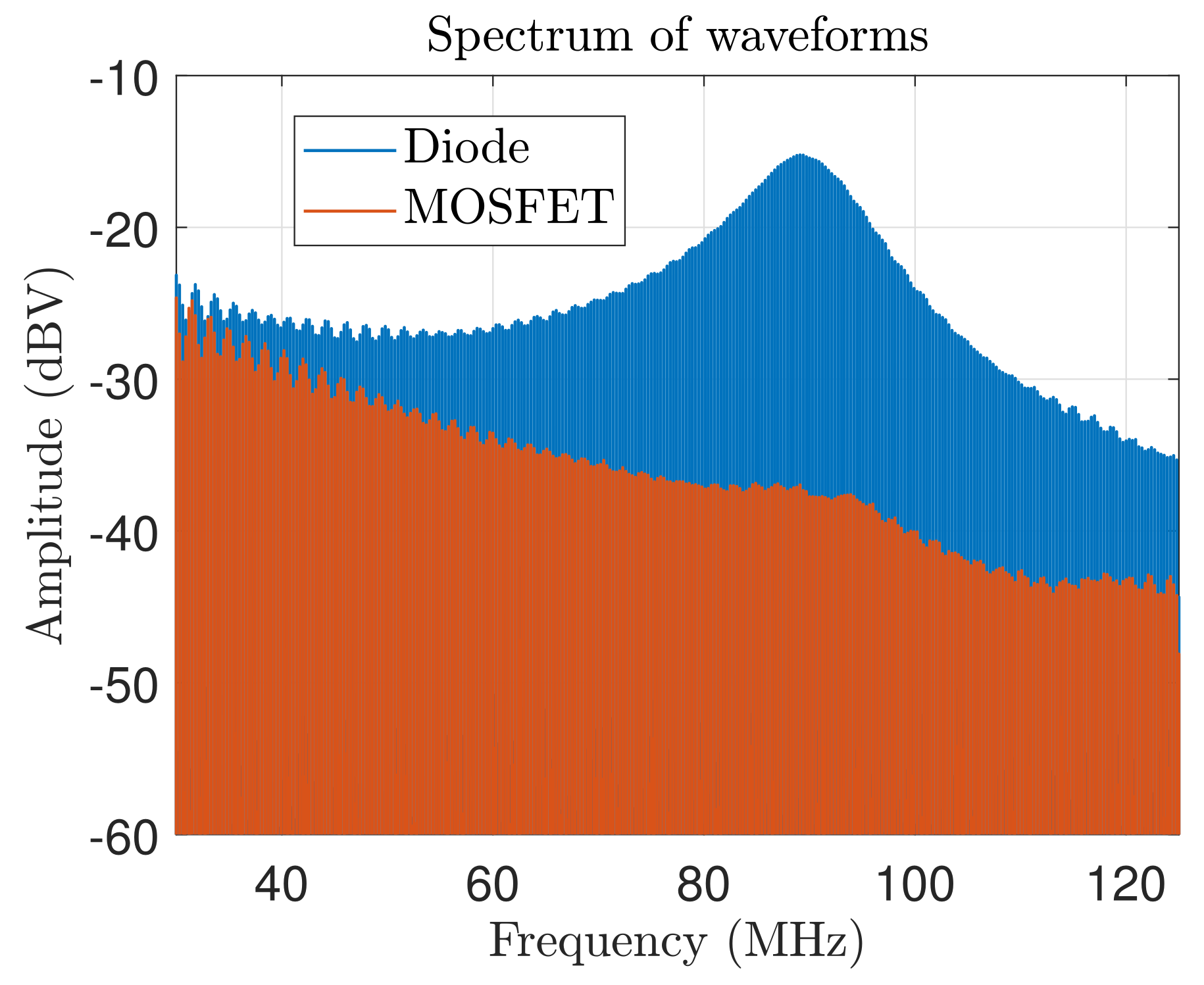
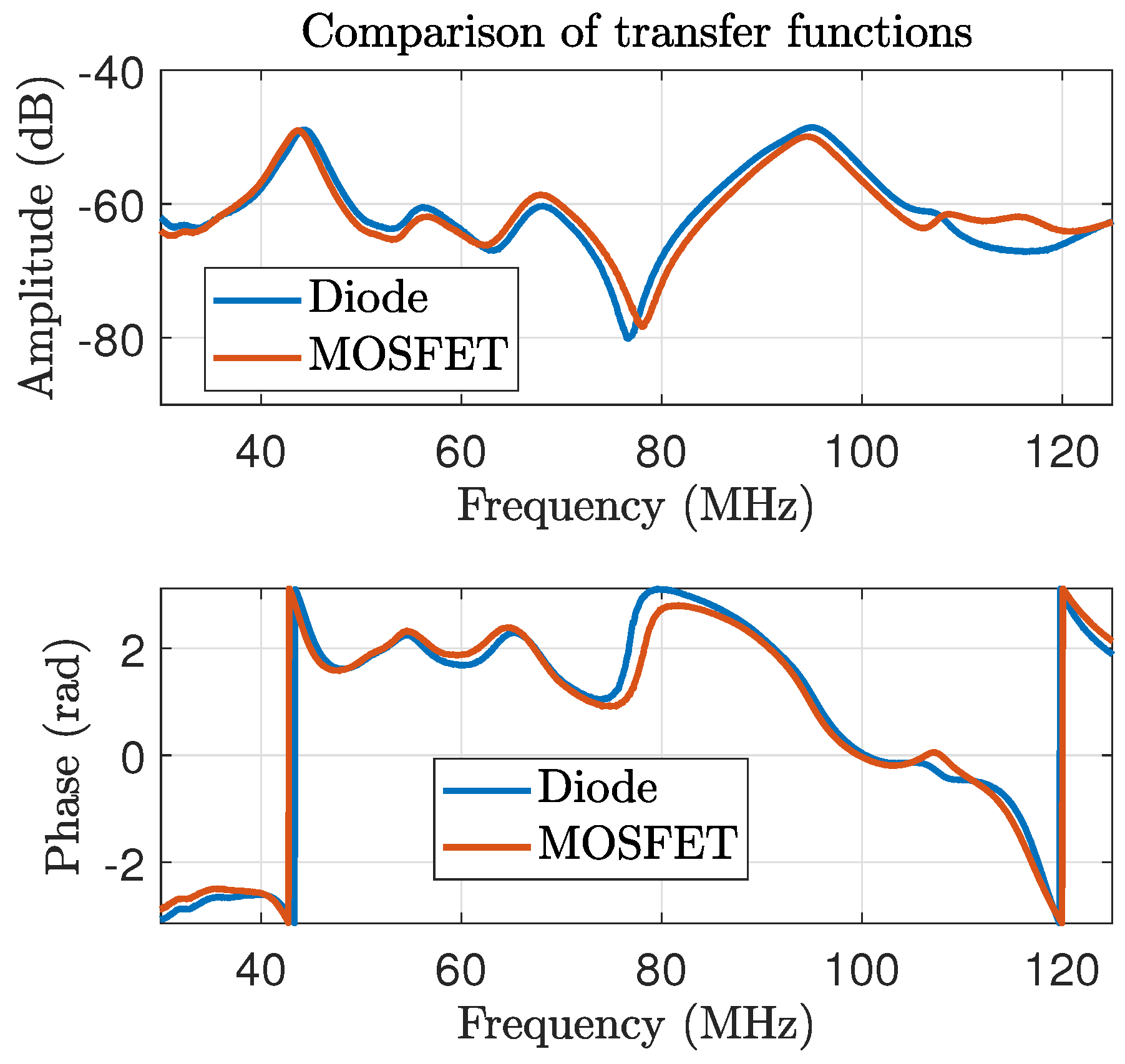
The spectra of the waveforms and corresponding transfer functions are presented in Figure 15 and Figure 16, which are used to predict the CM noise generated at the cable. The results show that the spectrum of the diode voltage is significantly higher than that of the MOSFET and is maximized at approximately 94 MHz. A dominant peak is expected in the CM noise, as the transfer functions are also maximized at the same frequency.
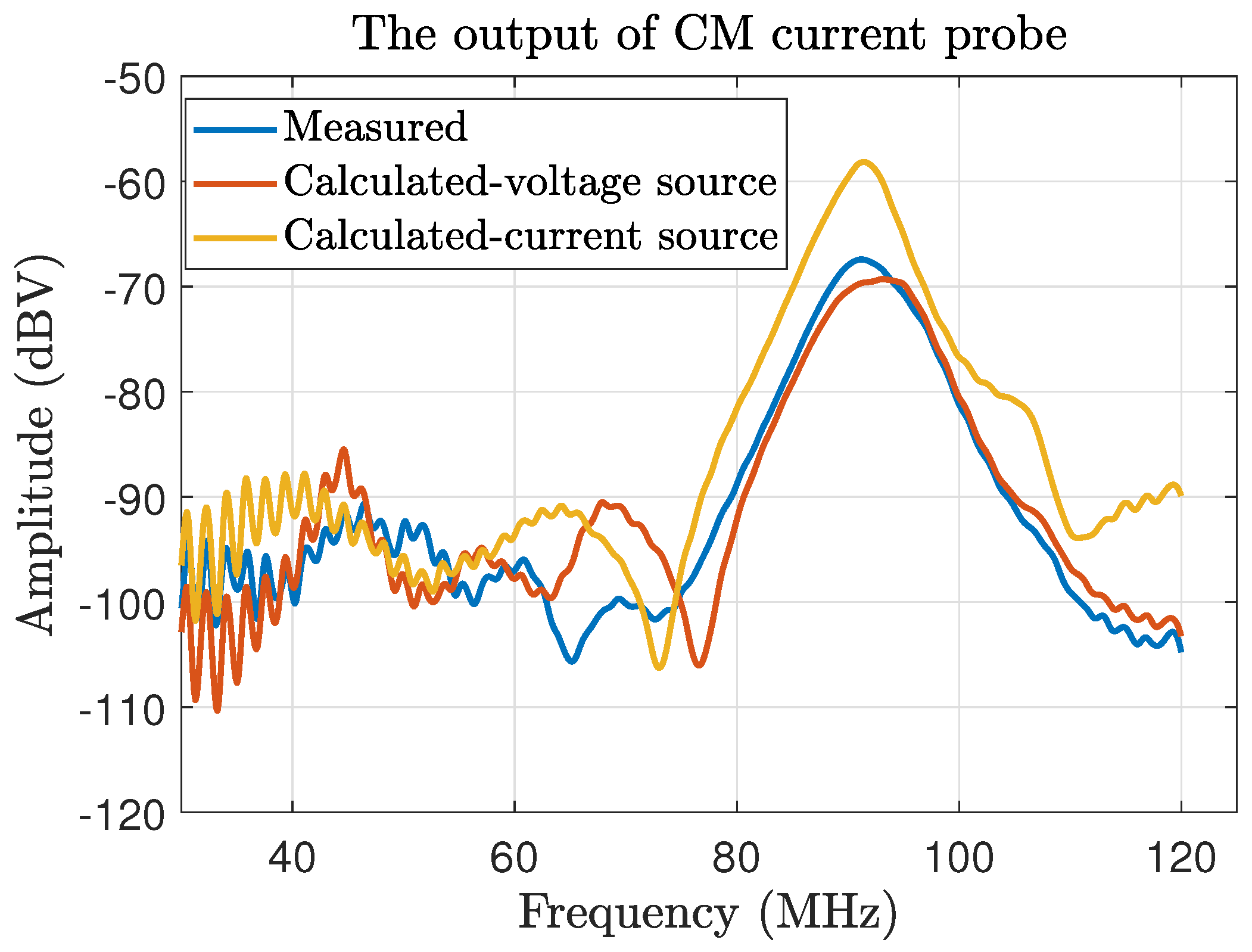
To validate the proposed CM noise estimation methodology, the calculated noise spectra are compared with experimentally measured data, as shown in Figure 17. For enhanced visualization, peak envelopes were extracted from the original spectra by applying cubic spline interpolation to local maxima identified at intervals of 500 samples. It is worth noting that both voltage source substitution and current source substitution approaches for diode modeling were evaluated to demonstrate optimal source selection in the equivalent circuit representation.
The voltage source substitution model exhibits superior correlation with the measured results, achieving CM noise predictions within 10 dB across the entire measurement bandwidth. Particularly, the discrepancies at dominant spectral peaks remain below 3 dB. Conversely, the current source substitution approach yields significantly higher errors, with peak deviations exceeding 10 dB at primary resonance frequencies. These findings highlight the critical importance of accurate current measurement in minimizing prediction errors when employing current source substitution techniques.
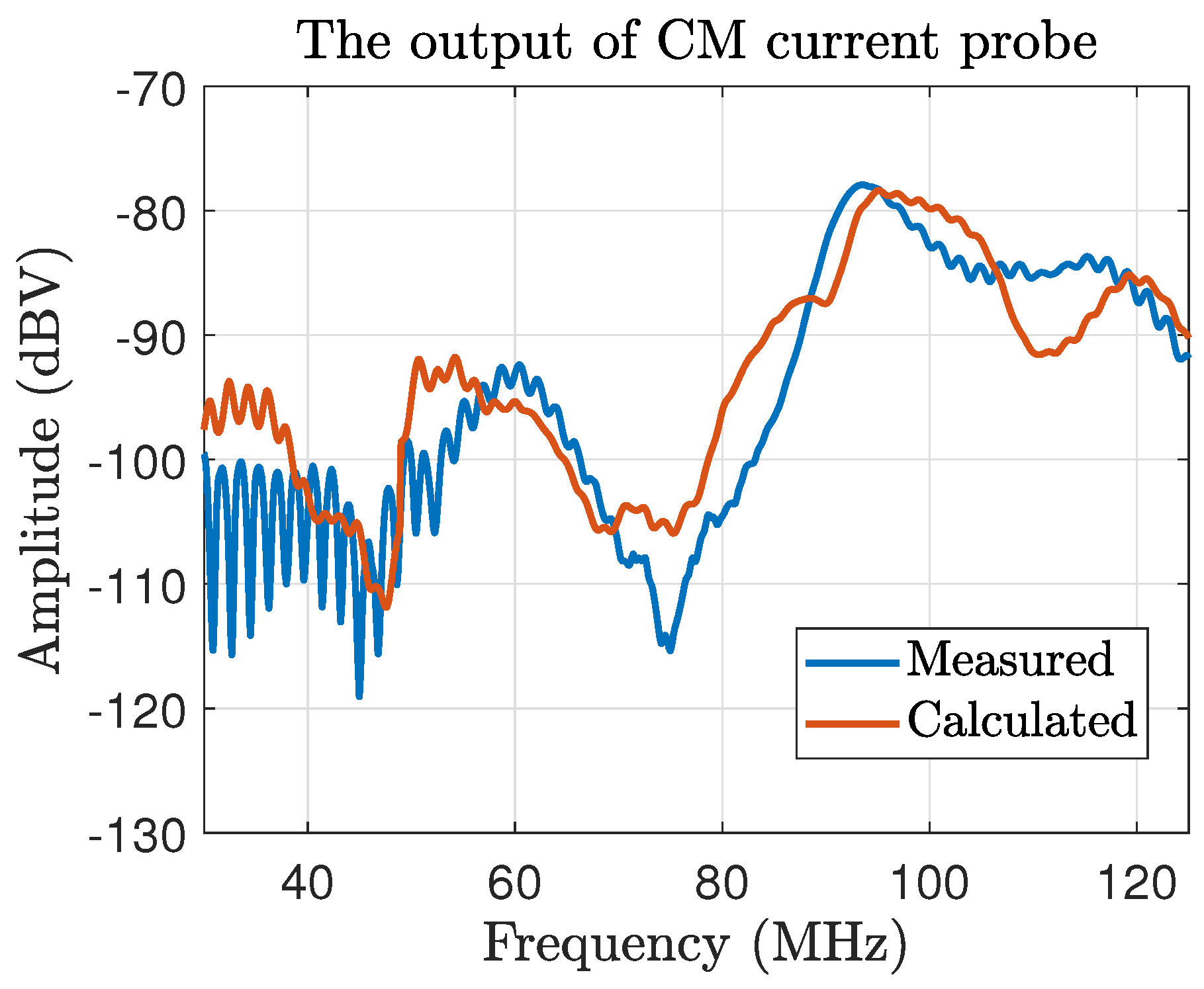
As further validation of the proposed method, the same CM noise estimation flow was applied with the current probe clamped on the input cables of the converter. As shown in Figure 18, good correlation was observed, with a maximum deviation of 6 dB. As an additional advantage of the proposed method, only the transfer functions need to be re-measured to estimate the location-dependent CM noise.

4. Dominant Noise Source Identification and Noise Mitigation Methods

In addition to estimating the noise generated by the converter, the proposed method is also an efficient tool for dominant noise localization. Noise generation mechanism can be identified and the corresponding mitigation methods can be strategically applied accordingly.

4.1. Noise Source Identification

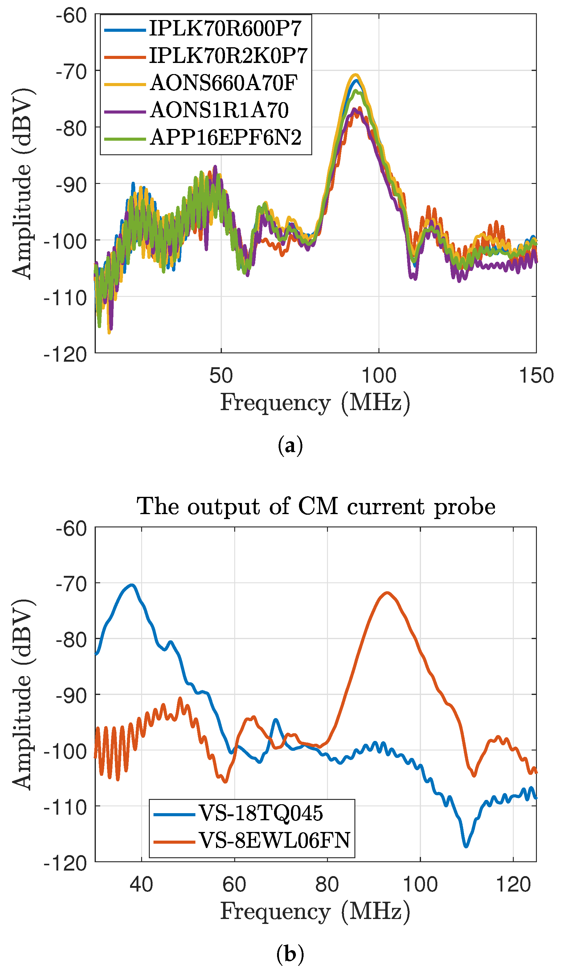
As shown in Figure 15 and Figure 16, the CM noise generated by the diode is much higher than that of the MOSFET. To further demonstrate the validity of this method, five different MOSFETs were installed on the board for comparison. The results are shown in Figure 19a. The positions of the boost converter, input and output cables, and CM current probe were fixed throughout the measurement.
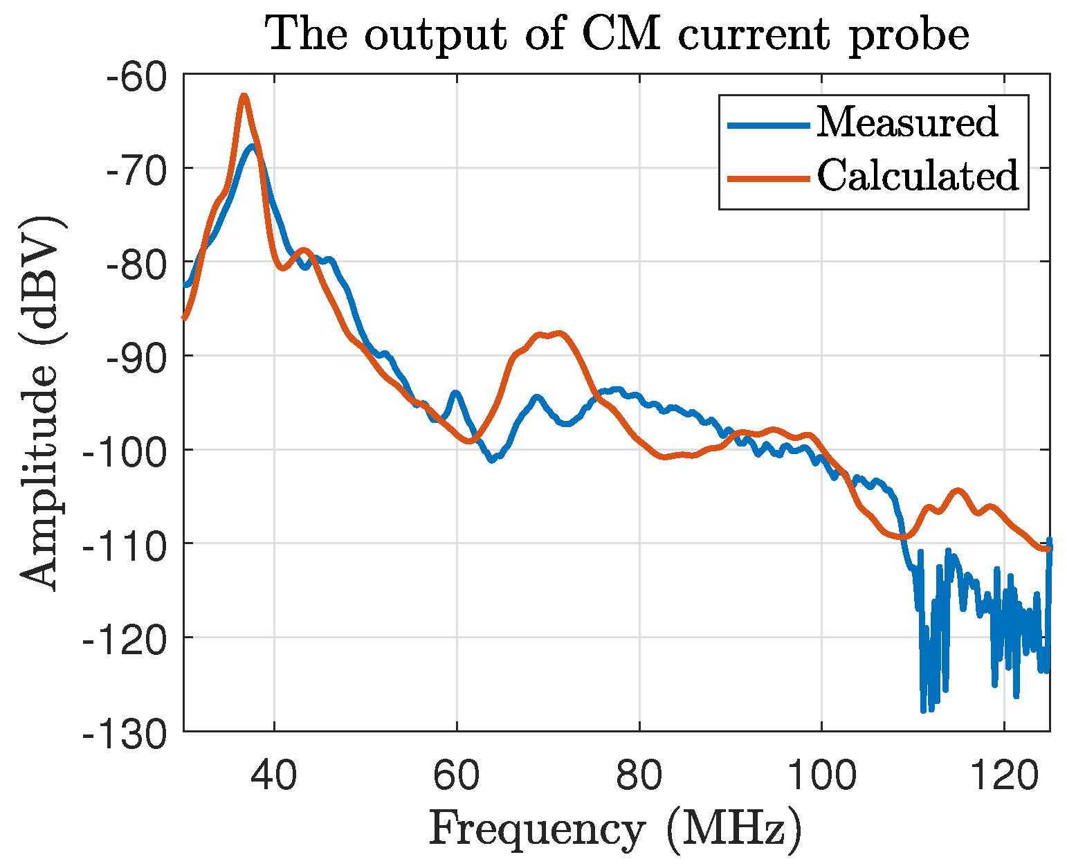
The deviation introduced by the different MOSFETs is limited to 8 dB and is primarily observed at 94 MHz. To further investigate this method, the diode installed on the board was replaced by a different unit (model: VS-18TQ045-M3). The dominant peak generated at the output cable shifted from 94 MHz to 36 MHz, proving that the dominant noise source is the diode.
For completeness of the method, Figure 20 compares the CM noise generated at the output cables after diode replacement. The errors between the measurement and calculation are within 6 dB for frequencies up to 110 MHz. The proposed method offers advantages over existing models that require accurate modeling of the PCB parasitics.

4.2. Noise Mitigation Techniques

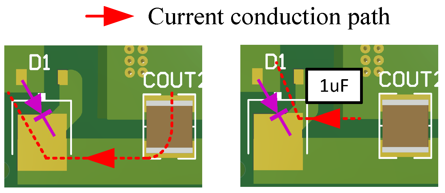
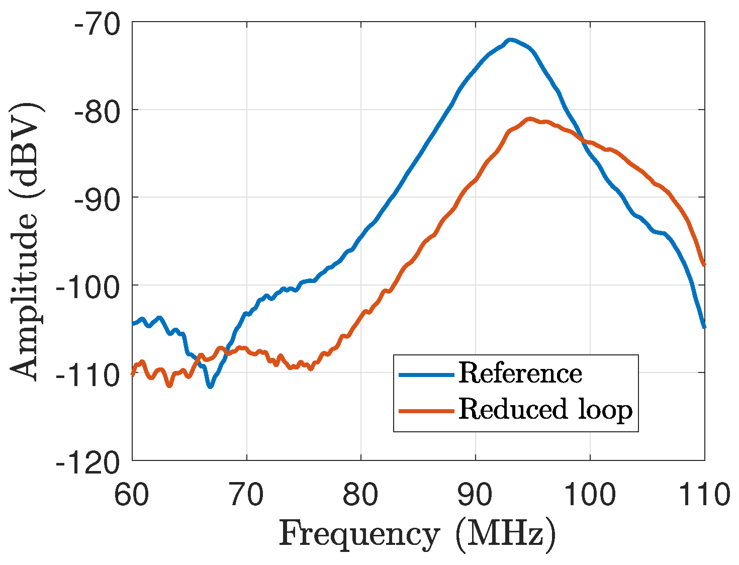
It has been demonstrated that the noise is primarily generated by the diode during the turn-on transition of the MOSFET. It can be concluded that the CM noise is produced by reverse recovery of the diode [18,19]. Thus, the conduction path of the reverse recovery current I R R is critical for the EMI performance, as illustrated in Figure 21. A noise mitigation method was applied by changing only the placement of the decoupling capacitors, and a noise reduction of 9 dB was observed for the improved layout at 94 MHz, as shown in Figure 22 and Figure 23. This experimental validation establishes a foundation for implementing advanced noise suppression techniques, such as multilayer PCB design for further loop size reduction.

5. Conclusions

This work presents a methodology for predicting CM noise emissions from boost converters with attached cabling through a substitution-based approach, where nonlinear switching components are replaced with independent voltage/current sources. The core innovation lies in the development of a measurement-based one-step transfer function extraction method, which achieves rapid CM noise estimation with less than 10 dB deviation across the 30–125 MHz bandwidth and dominant noise peaks predicted within 5 dB error under varying operational conditions, validated experimentally for configurations involving different semiconductor devices and cabling structures. Table 1 details the advantages and limitations of various existing and proposed modeling methodologies.
However, several limitations must be addressed to enable broader adoption of the proposed methodology: (1) Low-noise frequency range accuracy: Further investigation is required to enhance measurement precision in low-amplitude regions, particularly in optimizing the common-mode rejection ratio of the transfer function measurement setup; (2) Scalability constraints: the necessity to substitute all nonlinear switching devices with independent sources imposes significant procedural complexity on high-density topologies. This limitation becomes particularly pronounced in systems with multiple switching components (e.g., full-bridge LLC converters).

Author Contributions

Conceptualization, A.H.; methodology, A.H. and X.Z.; software, A.H. and Q.H.; validation, A.H., Q.H. and H.W.; formal analysis, A.H.; investigation, A.H.; resources, X.Z.; data curation, A.H.; writing—original draft preparation, A.H.; writing—review and editing, H.W. and Q.H.; visualization, A.H.; supervision, A.H.; project administration, A.H. All authors have read and agreed to the published version of the manuscript.

Funding

This research received no external funding.

Data Availability Statement

The data presented in this study are available on request from the authors.

Conflicts of Interest

The authors declare no conflicts of interest.

References

  1. Kim, K.; Shim, H.W.; Hwang, C. Analysis and Solution for RF Interference Caused by PMIC Noise in Mobile Platforms. IEEE Trans. Electromagn. Compat. 2019, 62, 682–690. [Google Scholar] [CrossRef]
  2. Shinde, S.; Masuda, K.; Shen, G.; Patnaik, A.; Makharashvili, T.; Pommerenke, D.; Khilkevich, V. Radiated EMI estimation from DC–DC converters with attached cables based on terminal equivalent circuit modeling. IEEE Trans. Electromagn. Compat. 2017, 60, 1769–1776. [Google Scholar] [CrossRef]
  3. Zhang, Y.; Wang, S.; Chu, Y. Analysis and Comparison of the Radiated Electromagnetic Interference Generated by Power Converters with Si MOSFET s and GaN HEMTs. IEEE Trans. Power Electron. 2020, 35, 8050–8062. [Google Scholar] [CrossRef]
  4. Yao, J.; Li, Y.; Wang, S.; Huang, X.; Lyu, X. Modeling and Reduction of Radiated EMI in a GaN IC-Based Active Clamp Flyback Adapter. IEEE Trans. Power Electron. 2020, 36, 5440–5449. [Google Scholar] [CrossRef]
  5. Zhang, J.; Lu, T.; Zhang, W.; Bian, X.; Cui, X. Characteristics and influence factors of radiated disturbance induced by IGBT switching. IEEE Trans. Power Electron. 2019, 34, 11833–11842. [Google Scholar] [CrossRef]
  6. Sangwan, V.; Kapoor, D.; Tan, C.M.; Lin, C.H.; Chiu, H.C. High-frequency electromagnetic simulation and optimization for GaN-HEMT power amplifier IC. IEEE Trans. Electromagn. Compat. 2018, 61, 564–571. [Google Scholar] [CrossRef]
  7. Park, H.H.; Park, H.B.; Lee, H.S. A simple method of estimating the radiated emission from a cable attached to a mobile device. IEEE Trans. Electromagn. Compat. 2012, 55, 257–264. [Google Scholar] [CrossRef]
  8. Oswald, N.; Anthony, P.; McNeill, N.; Stark, B.H. An experimental investigation of the tradeoff between switching losses and EMI generation with hard-switched all-Si, Si-SiC, and all-SiC device combinations. IEEE Trans. Power Electron. 2013, 29, 2393–2407. [Google Scholar] [CrossRef]
  9. Bishnoi, H.; Mattavelli, P.; Burgos, R.; Boroyevich, D. EMI behavioral models of DC-fed three-phase motor drive systems. IEEE Trans. Power Electron. 2013, 29, 4633–4645. [Google Scholar] [CrossRef]
  10. Song, C.; Kim, H.; Kim, Y.; Kim, D.; Jeong, S.; Cho, Y.; Lee, S.; Ahn, S.; Kim, J. EMI reduction methods in wireless power transfer system for drone electrical charger using tightly coupled three-phase resonant magnetic field. IEEE Trans. Ind. Electron. 2018, 65, 6839–6849. [Google Scholar] [CrossRef]
  11. Shen, G.; Shinde, S.; Patnaik, A.; Pommerenke, D.; Aichele, H.; Keller, C.; Boettcher, M.; Khilkevich, V. Terminal modeling of DC–DC converters with stochastic behavior. IEEE Trans. Electromagn. Compat. 2018, 60, 2011–2018. [Google Scholar] [CrossRef]
  12. Bishnoi, H.; Baisden, A.C.; Mattavelli, P.; Boroyevich, D. Analysis of EMI terminal modeling of switched power converters. IEEE Trans. Power Electron. 2012, 27, 3924–3933. [Google Scholar] [CrossRef]
  13. Liu, D.; Wang, Y.; Kautz, R.W.; Altunyurt, N.; Chandra, S.; Fan, J. Accurate evaluation of field interactions between cable harness and vehicle body by a multiple scattering method. IEEE Trans. Electromagn. Compat. 2016, 59, 383–393. [Google Scholar] [CrossRef]
  14. Wang, S.; Kong, P.; Lee, F.C. Common mode noise reduction for boost converters using general balance technique. IEEE Trans. Power Electron. 2007, 22, 1410–1416. [Google Scholar] [CrossRef]
  15. Yao, J.; Wang, S.; Luo, Z. Modeling, Analysis, and Reduction of Radiated EMI Due to the Voltage across Input and Output Cables in an Automotive Non-isolated Power Converter. IEEE Trans. Power Electron. 2021, 37, 5455–5465. [Google Scholar] [CrossRef]
  16. Pozar, D.M. Microwave Engineering; John Wiley & Sons: Hoboken, NJ, USA, 2011. [Google Scholar]
  17. Huang, A.; Wang, X.; Zhang, H.; Hwang, C.; Pommerenke, D.; Fan, J. Improved Current Shut Characterization Method for Ferrite Loss Characterization. IEEE Trans. Power Electron. 2022, 37, 8290–8300. [Google Scholar] [CrossRef]
  18. Zhao, Q.; Tao, F.; Lee, F.C.; Xu, P.; Wei, J. A simple and effective method to alleviate the rectifier reverse-recovery problem in continuous-current-mode boost converters. IEEE Trans. Power Electron. 2001, 16, 649–658. [Google Scholar] [CrossRef]
  19. Yuan, X.; Walder, S.; Oswald, N. EMI generation characteristics of SiC and Si diodes: Influence of reverse-recovery characteristics. IEEE Trans. Power Electron. 2014, 30, 1131–1136. [Google Scholar] [CrossRef]
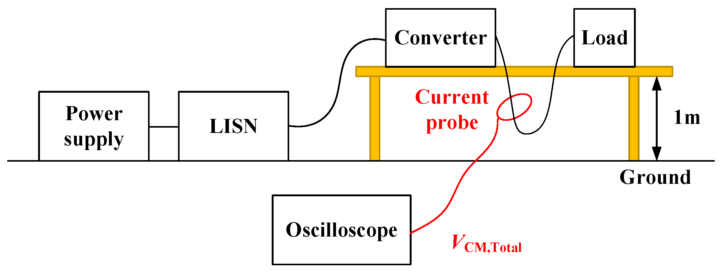
Figure 1. Configuration of the measurement setup. Two 1.5 m cables are used for both the input and output sides, and the CM current is measured by an RF current probe. The current probe is connected to an oscilloscope with an input impedance of 50 Ω .
Electronics 14 03375 g001
Figure 2. EMI model for a boost converter.
Electronics 14 03375 g002
Figure 3. Original equivalent substituted circuit model of a boost converter.
Electronics 14 03375 g003
Figure 4. Simplified circuits of CM current analysis. (a) Equivalent circuit for finding out the CM noise I C M , M O S due to V M O S . (b) Equivalent circuit for finding out the CM noise I C M , D due to I D .
Electronics 14 03375 g004
Figure 5. Measurement setup for the transfer function from the MOSFET to the current probe.
Electronics 14 03375 g005
Figure 6. Equivalent circuits for a voltage source excitation case.
Electronics 14 03375 g006
Figure 7. Flowchart for CM noise estimation.
Electronics 14 03375 g007
Figure 8. Comparison of current-to-voltage gain with and without considering the parasitic inductance.
Electronics 14 03375 g008
Figure 9. Improved equivalent substitution circuit model of a boost converter.
Electronics 14 03375 g009
Figure 10. Configuration of port 1 in the measurement. Calibration was performed with respect to the end of the semi-rigid cable.
Electronics 14 03375 g010
Figure 11. Measurement configurations and comparison of S21 responses under varying port1 polarization states.
Electronics 14 03375 g011
Figure 12. Photograph of the measurement setup.
Electronics 14 03375 g012
Figure 13. Circuit diagram of the boost converter under the default configuration. The switching frequency of the converter is configured as 300 kHz.
Electronics 14 03375 g013
Figure 14. Time -domain waveforms of V M O S and V D . (a) Waveforms during the turn-on period of the MOSFET. (b) Magnified waveforms during the turn-on transition.
Electronics 14 03375 g014
Figure 15. Spectra of V M O S and V D .
Electronics 14 03375 g015
Figure 16. Measured transfer functions for the MOSFET and diode.
Electronics 14 03375 g016
Figure 17. Comparison between the measured and calculated CM noise produced at the output cables.
Electronics 14 03375 g017
Figure 18. Comparison between the measured and calculated CM noise generated at the input cable.
Electronics 14 03375 g018
Figure 19. Comparison of CM noise measured at the output cables for different semiconductor devices. (a) Five different MOSFETs (Infineon: IPLK70R600P7 and IPLK70R2K0P7; Alpha and Omega: AONS660A70F and AONS1R1A70; ST: APP16EPF6N2). (b) Two different diodes (Vishay: VS-18TQ045-M3 and VS-8EWL06FN-M3).
Electronics 14 03375 g019
Figure 20. Comparison of measured and calculated CM noise generated at the input cable.
Electronics 14 03375 g020
Figure 21. Current conduction paths during the reverse recovery period.
Electronics 14 03375 g021
Figure 22. Initial layout of the boost converter and an improved layout with a smaller current conduction loop.
Electronics 14 03375 g022
Figure 23. CM noise measured at the output cables.
Electronics 14 03375 g023
Table 1. Comparative analysis of CM noise estimation techniques.
Estimation MethodAdvantages/MeritsLimitations
Two-step Method ([15])
  • Enables noise transfer function estimation in the layout stage.
  • Can be used for pre-design analysis.
  • Time consuming to build and verify the model.
  • Computationally expensive.
  • Accuracy of the method can be influenced by the placement of cables.
One-step Method (This work)
  • Enables a fast and in-situ noise transfer function measurement.
  • Can be applied when the simulation model is not provided.
  • Need further work to solve the scalability issues for power converter with large number of switching devices.
  • Accuracy in the low amplitude region need improvement.
Disclaimer/Publisher’s Note: The statements, opinions and data contained in all publications are solely those of the individual author(s) and contributor(s) and not of MDPI and/or the editor(s). MDPI and/or the editor(s) disclaim responsibility for any injury to people or property resulting from any ideas, methods, instructions or products referred to in the content.