
Research on the Evaluation Method of Electrical Stress Limit Capability Based on Reliability Enhancement Theory


Abstract
1. Introduction
2. Test Design Methodology for 3D-Packaged Memory Limit Capability Evaluation
2.1. Research on the Test Profile for Electrical Stress Limit Testing
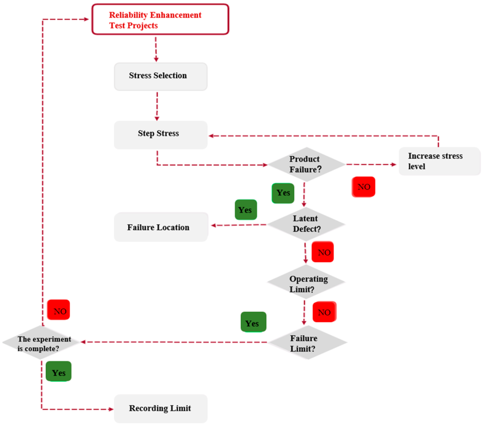
2.1.1. Research on the Test Profile for Electrical Stress Limit Testing
- (1)
- Power Voltage Limit Test Profile
- (2)
- Input Clock Frequency Limit Test Profile
- (3)
- Electrostatic Discharge (ESD) Sensitivity Limit Test Profile
- (4)
- Electrical Endurance Limit Test Profile
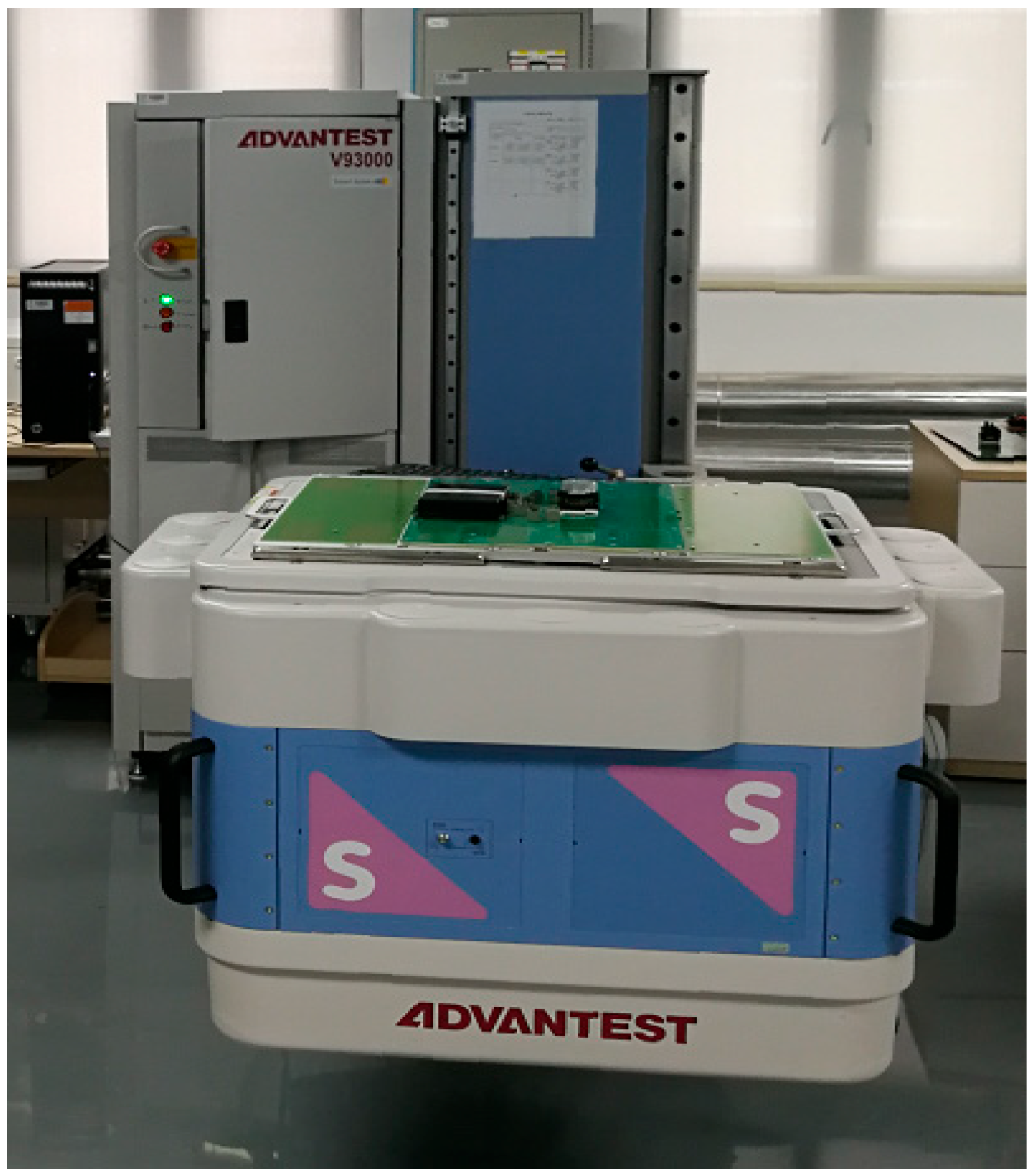
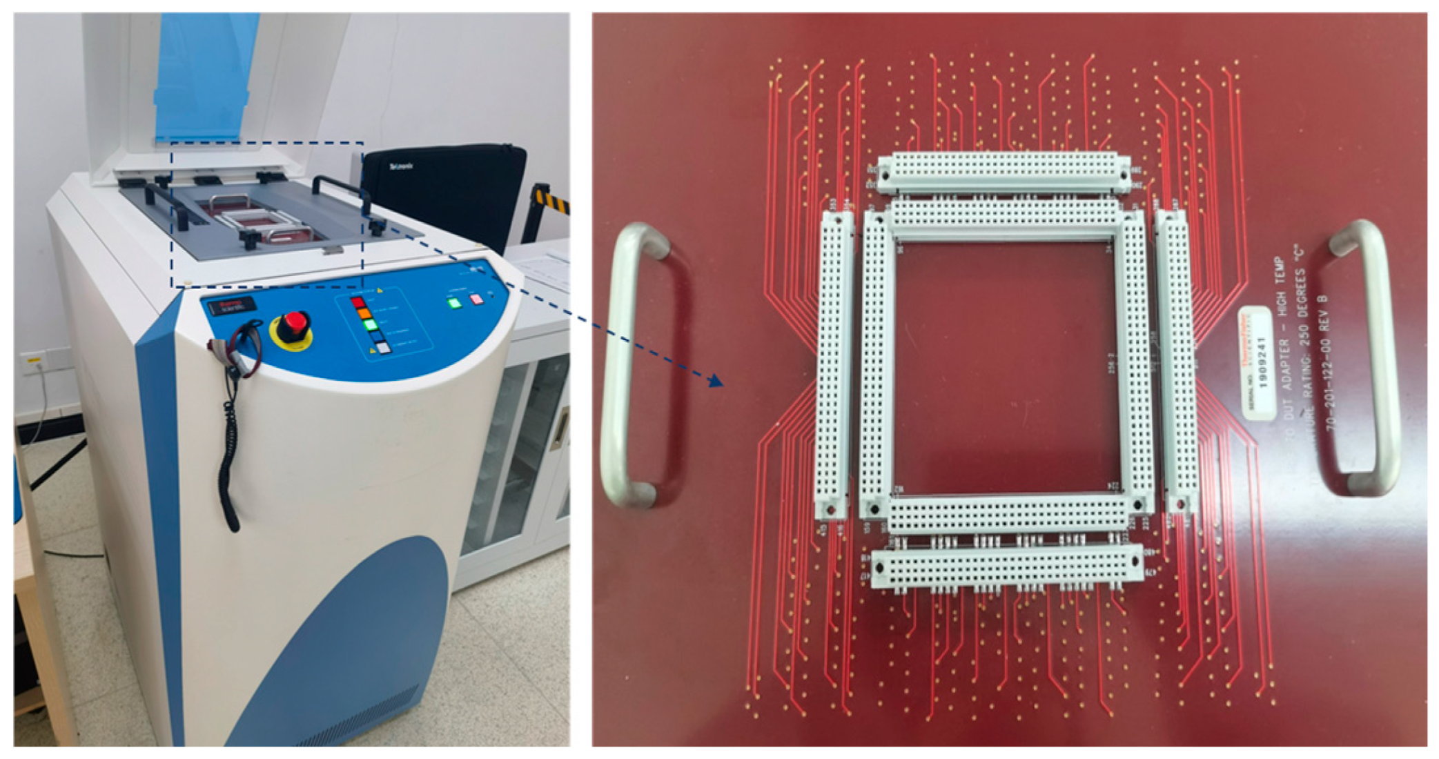
2.1.2. Construction of Electrical Stress Testing Equipment (Equipment Description)
- (1)
- ATE Tester
- (2)
- Electrostatic Discharge (ESD) Sensitivity Tester
2.1.3. Principles of 3D-Packaged Memory Limit Capability Testing
- (1)
- Scan Path Testing
- (2)
- Built-In Self-Test (BIST) Method [13]
- (3)
- Boundary Scan Testing
3. Research on Functional Performance Testing Methods for 3D-Packaged Memory
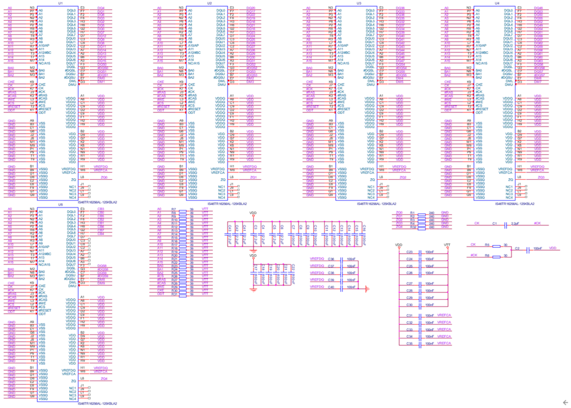
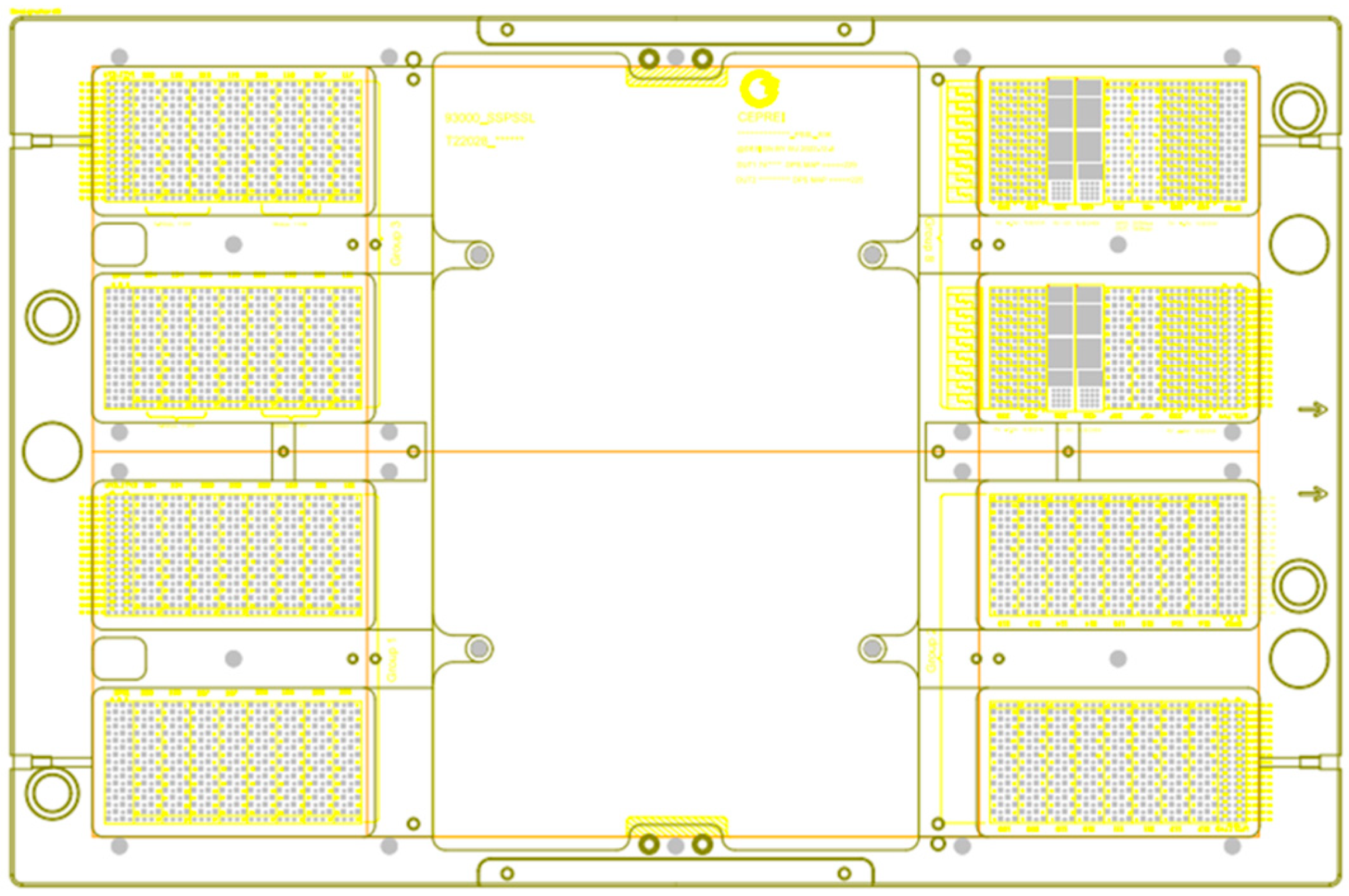
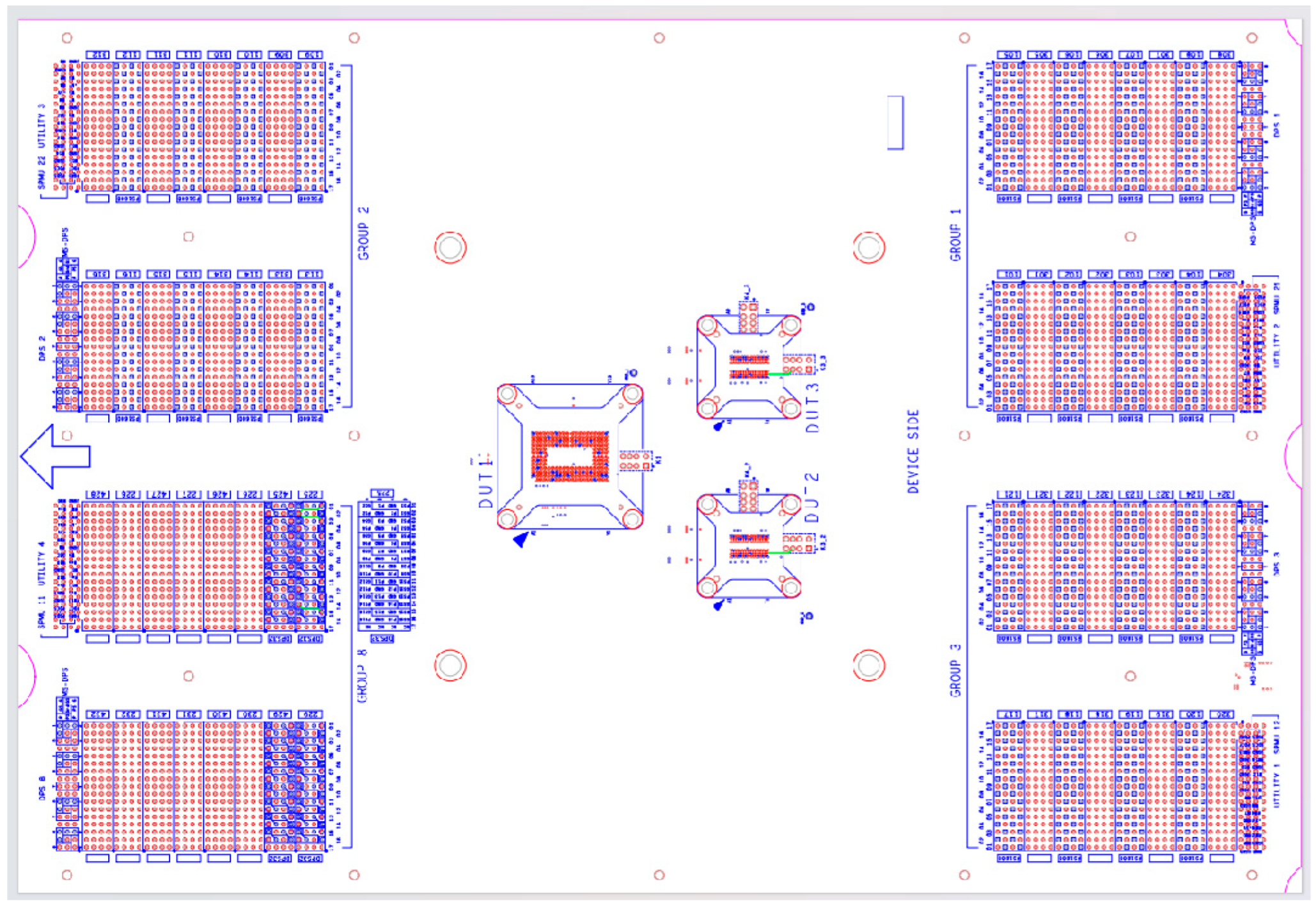
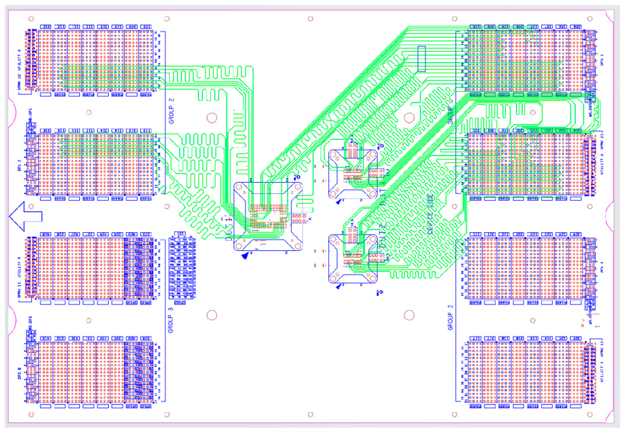
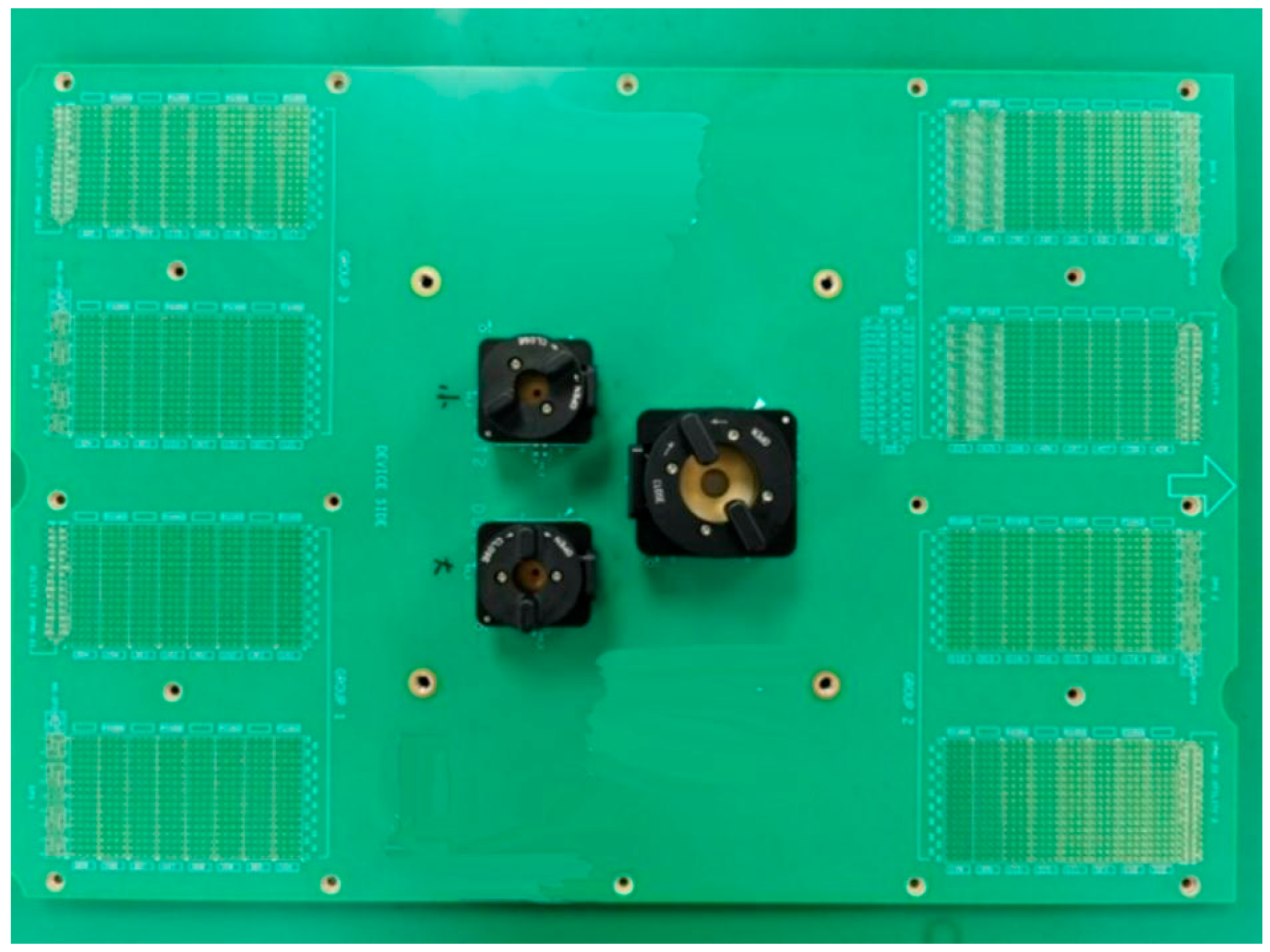
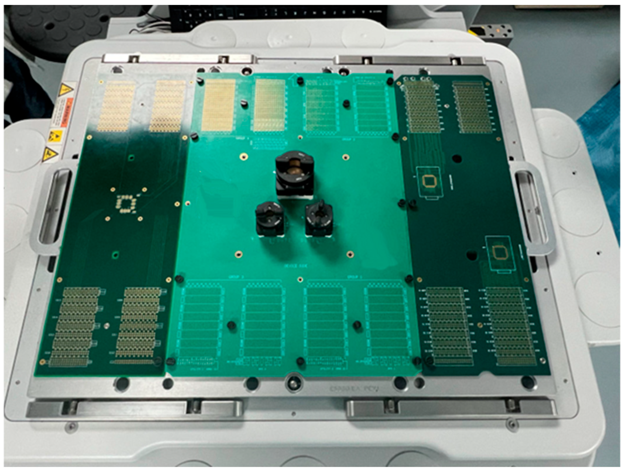
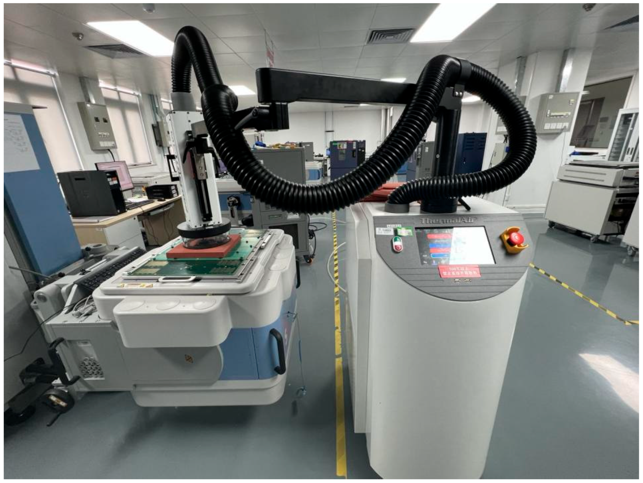
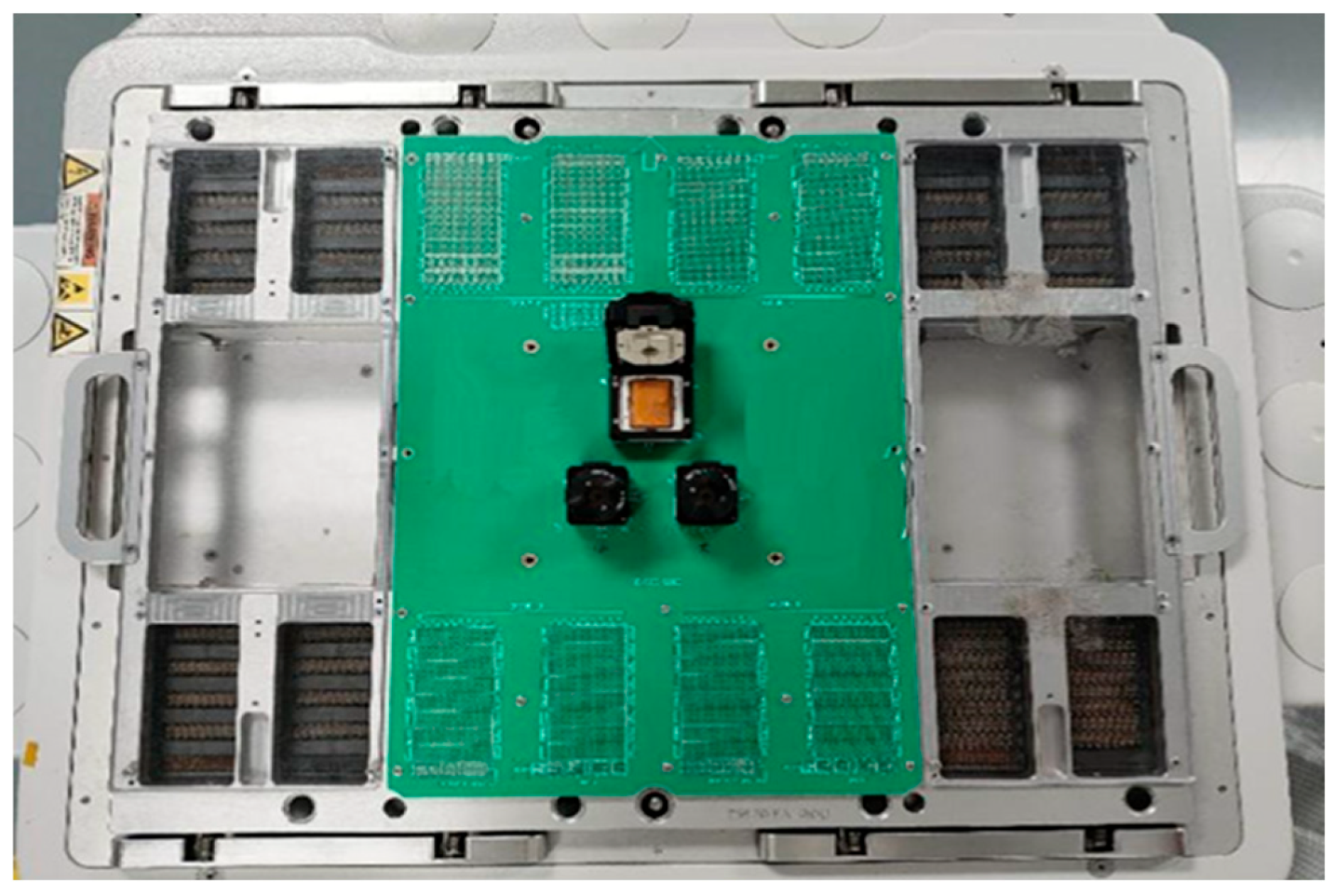
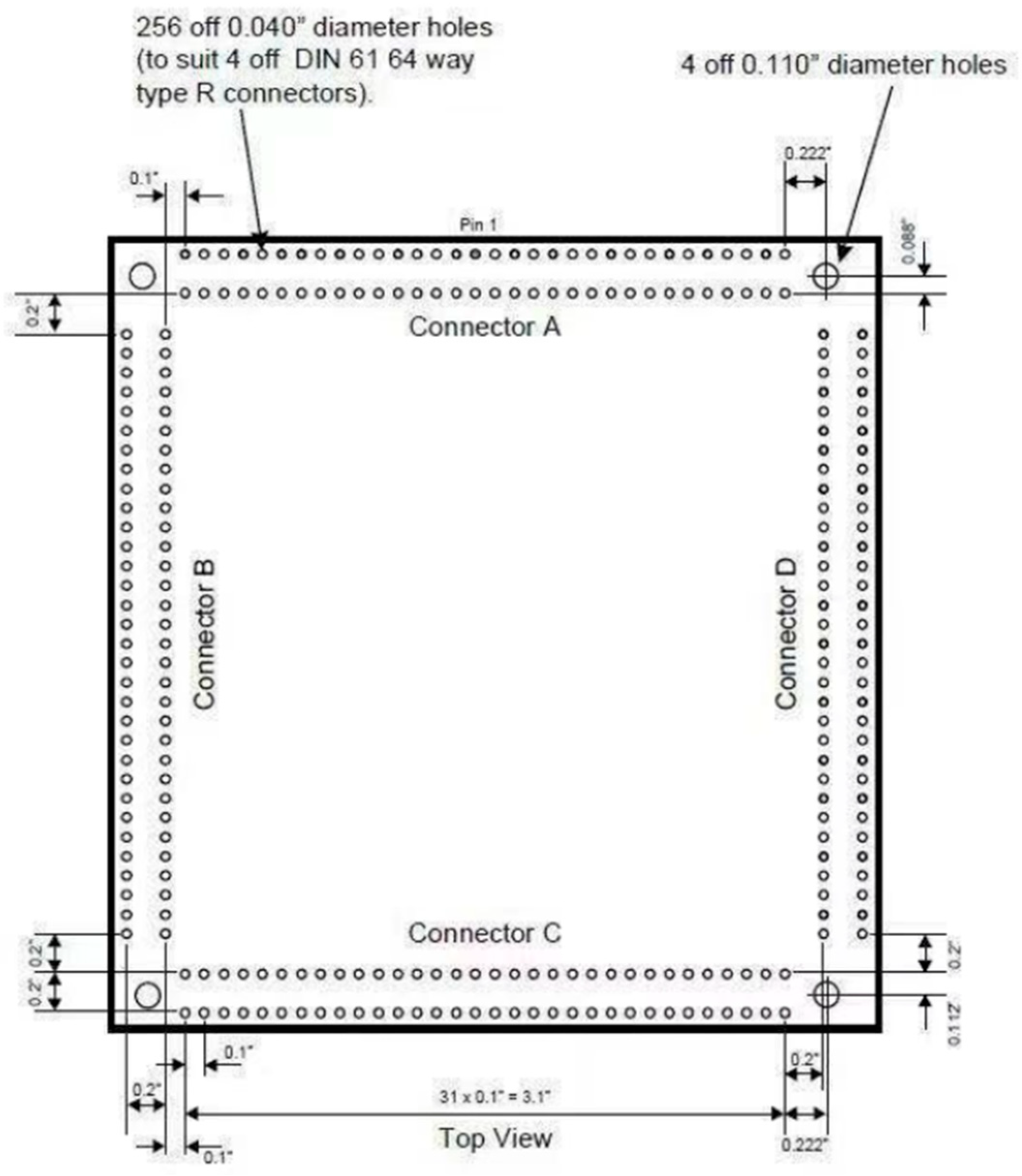
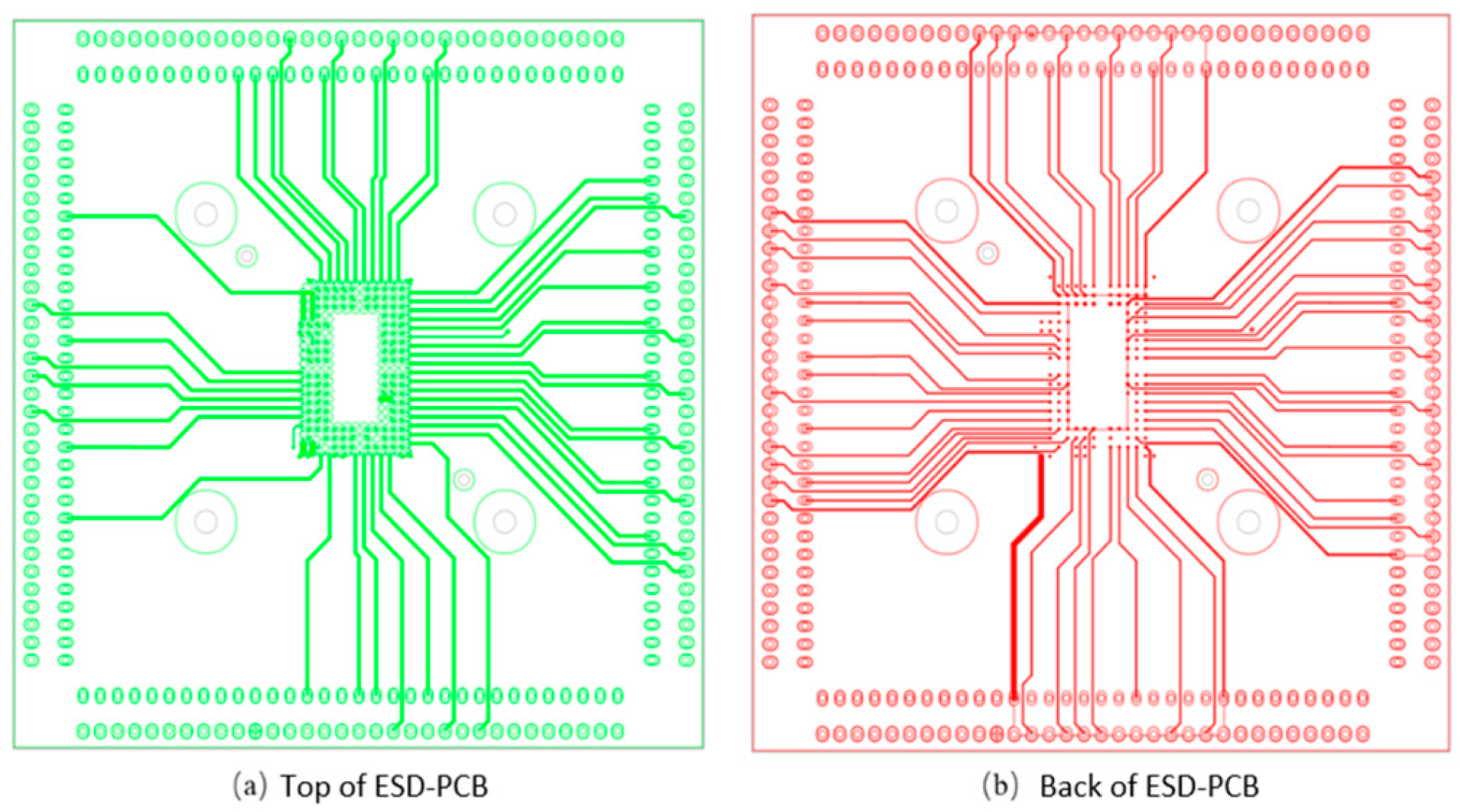
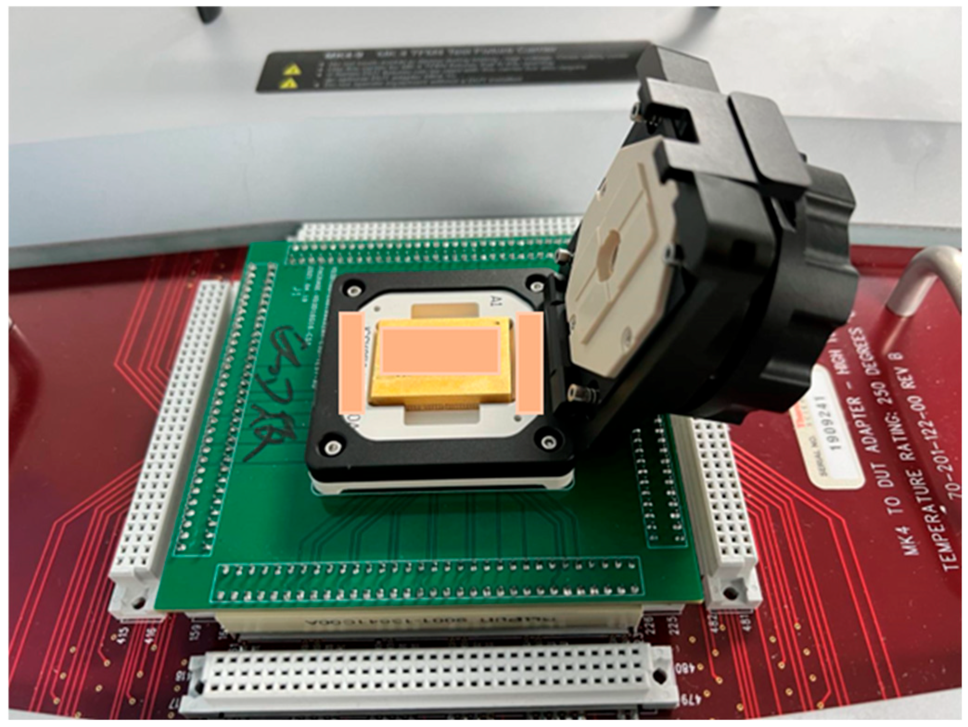
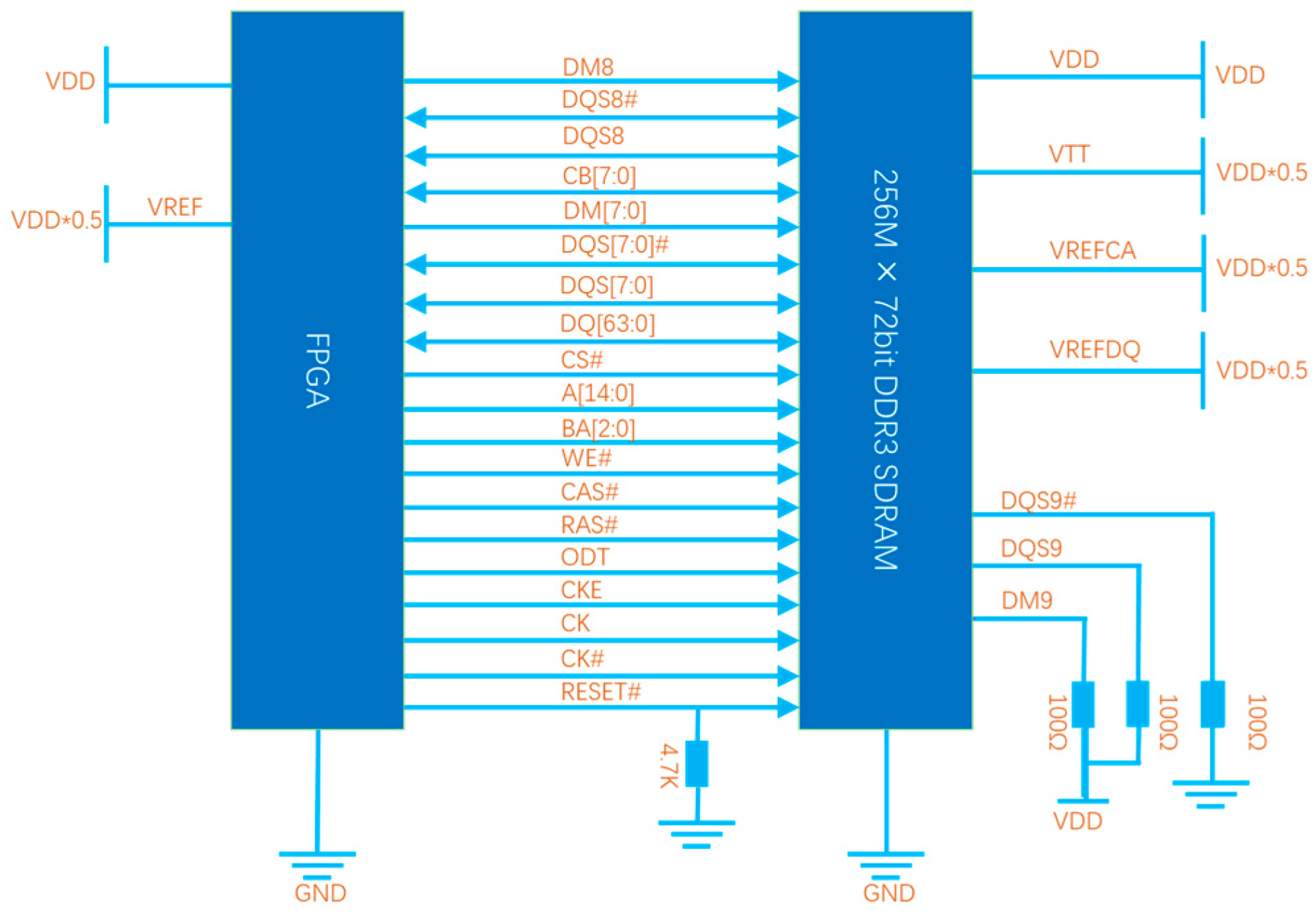
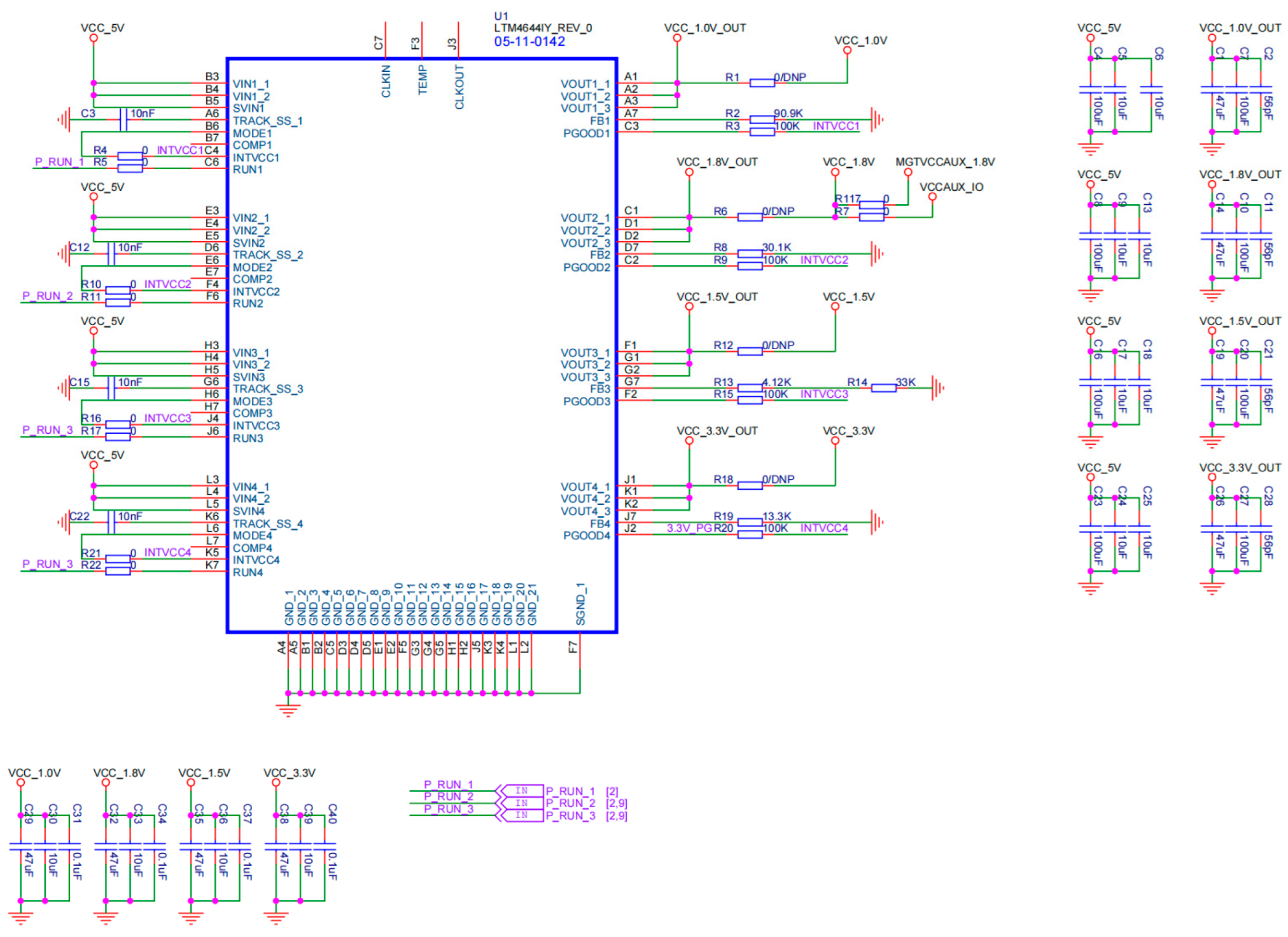
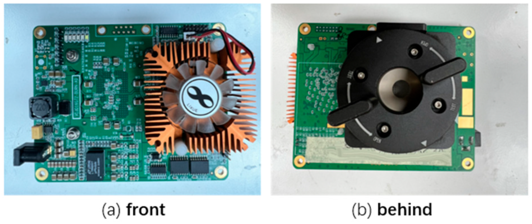
3.1. Construction of Functional Performance Testing Platform and PCB Design for 3D-Packaged Memory
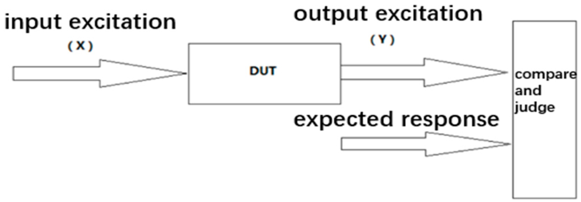
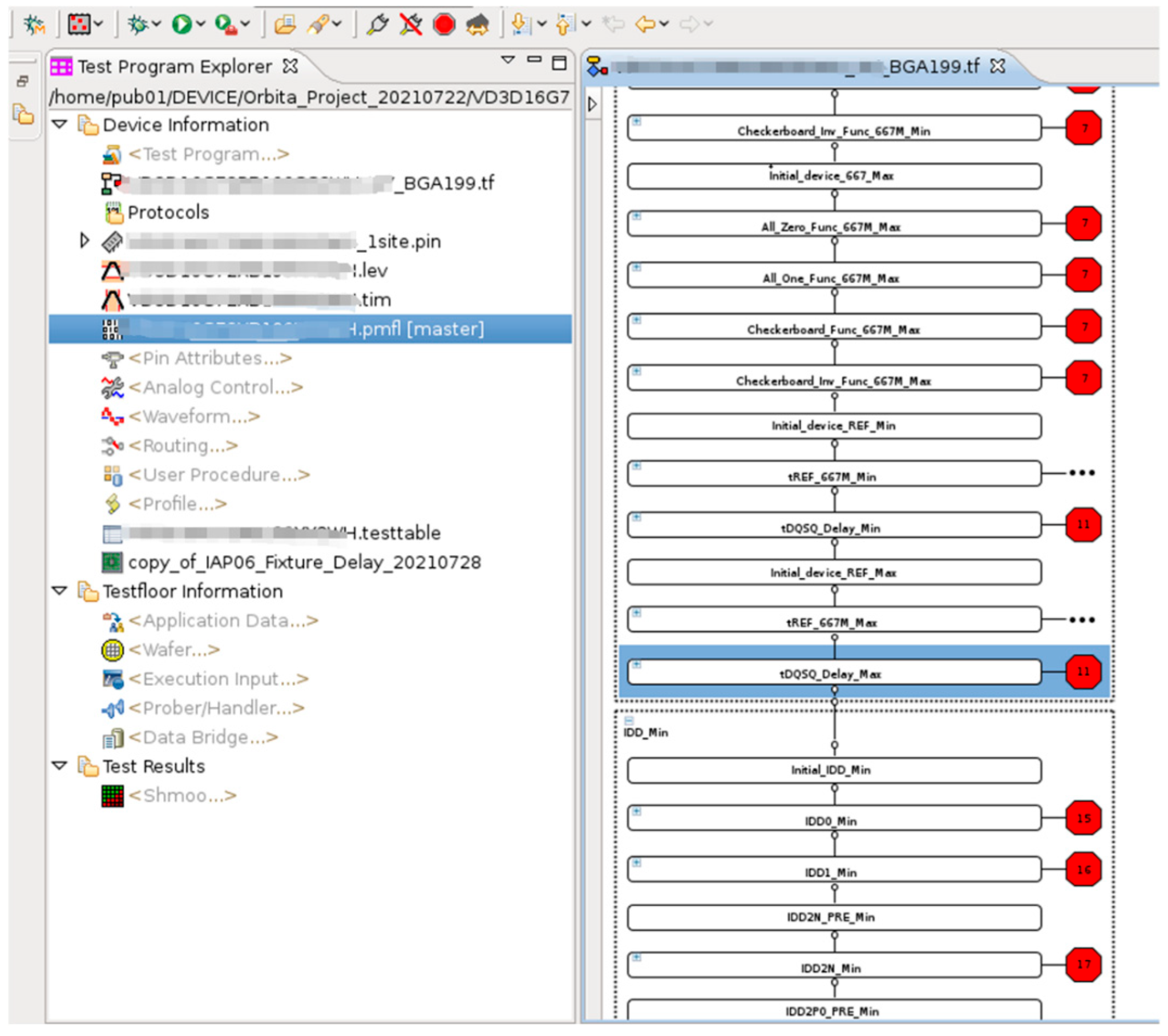
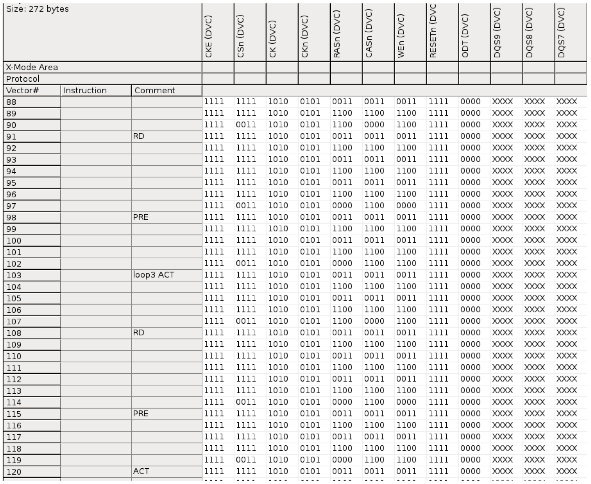
3.2. Three-Dimensional-Packaged Memory Functional Performance Testing Methods
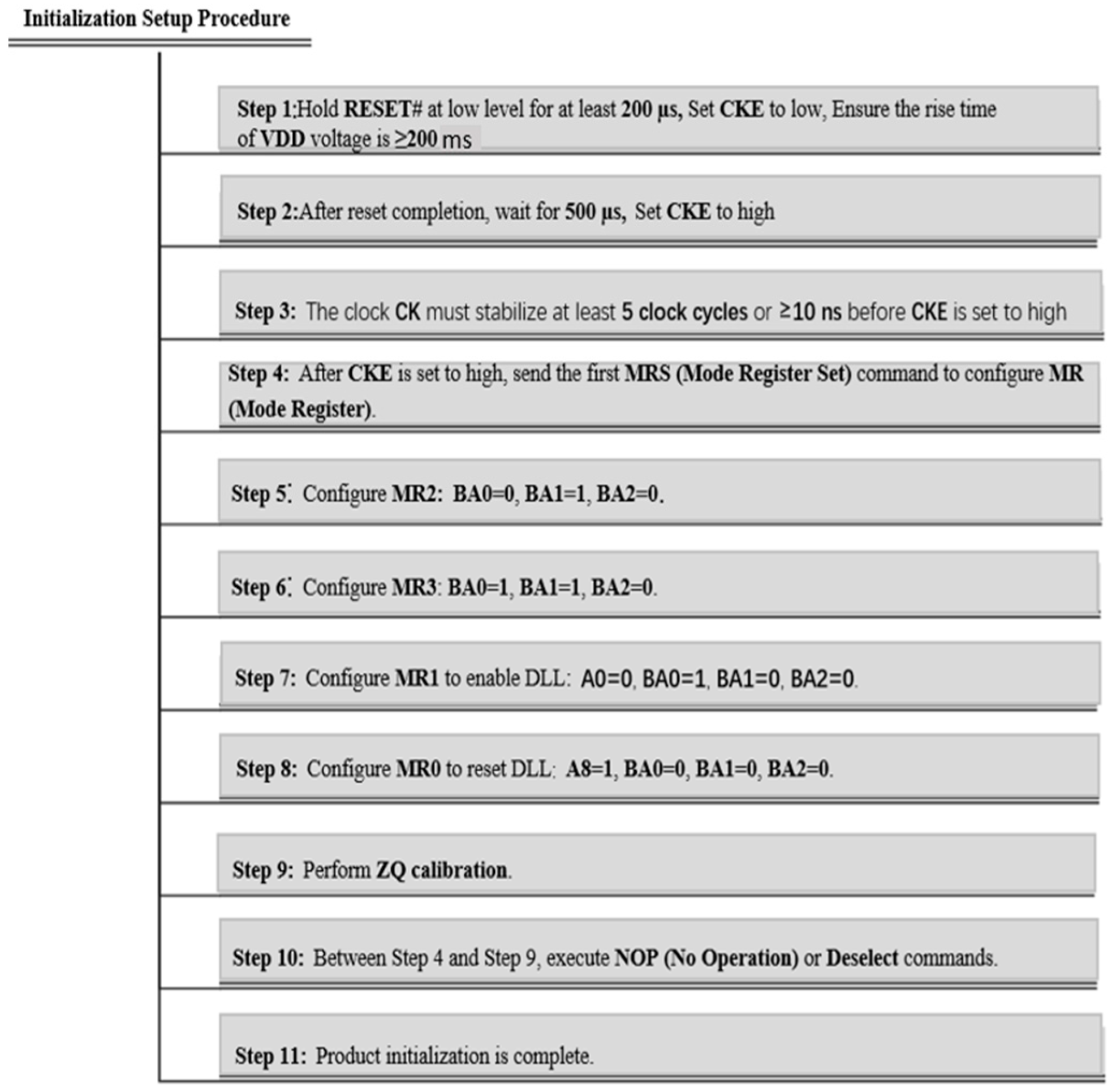
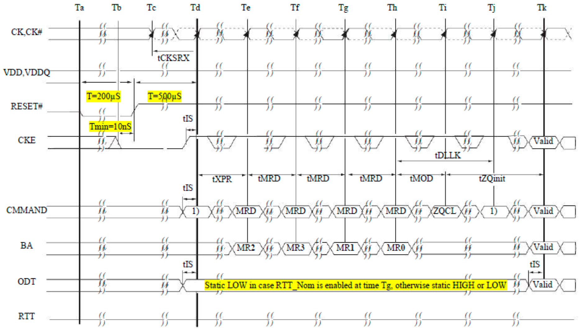
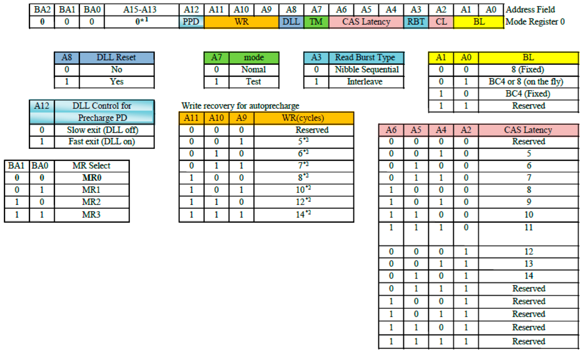
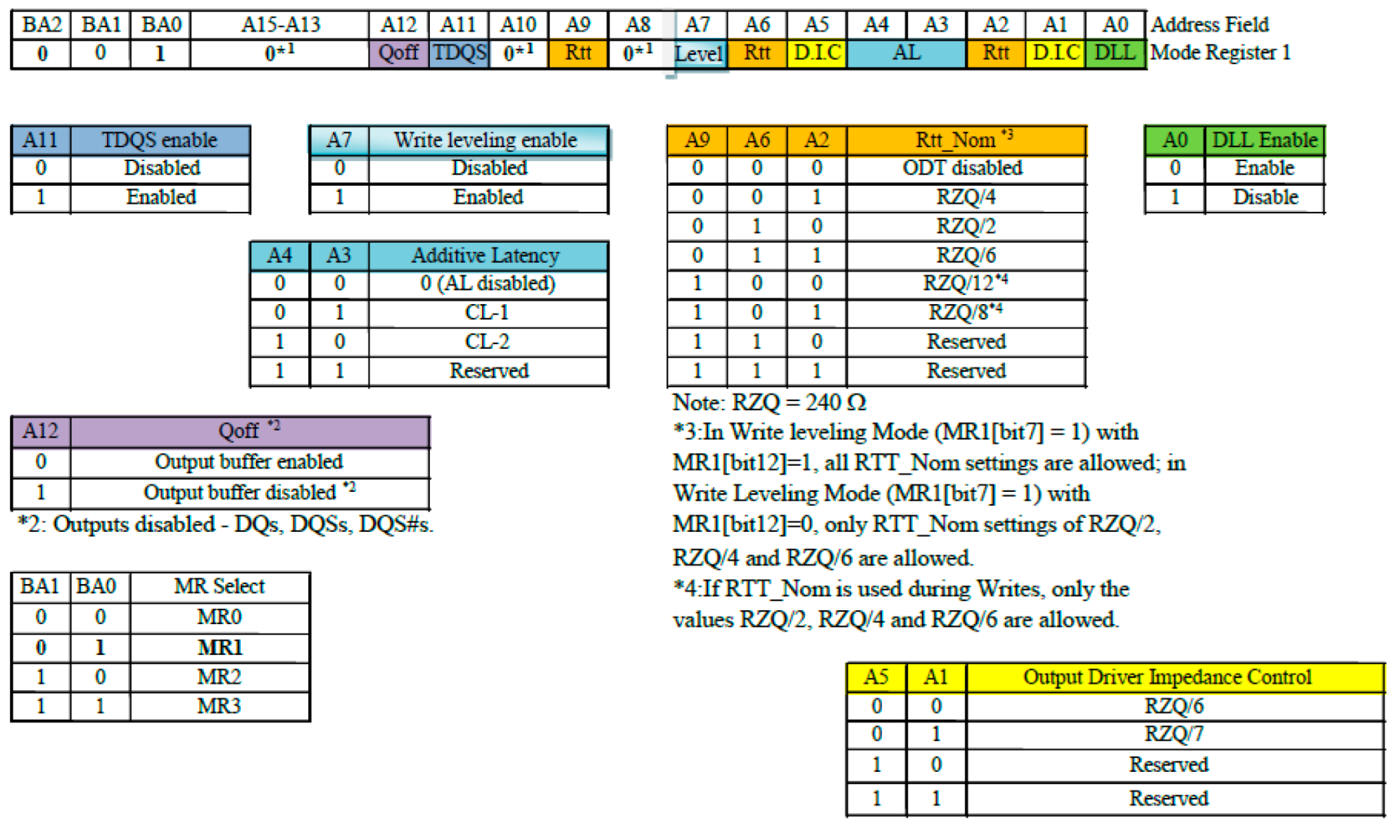
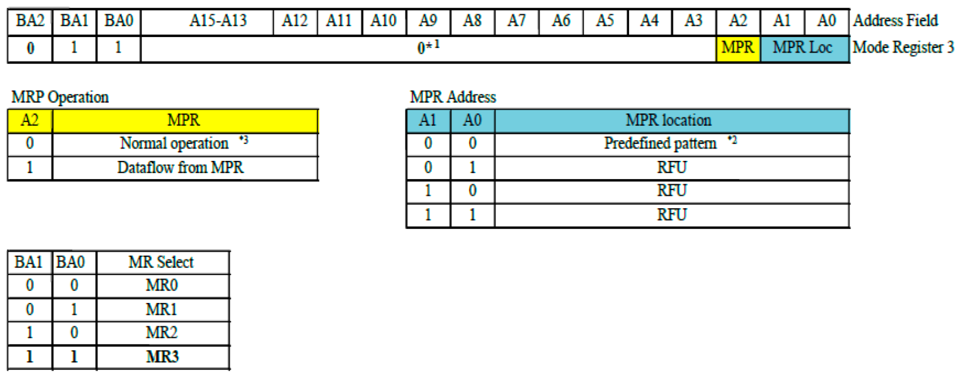
3.2.1. Initialization Setup Methods for Functional Performance Testing
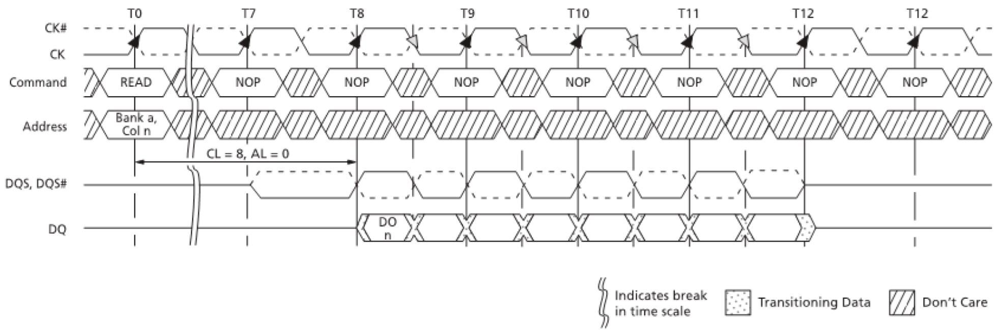
3.2.2. Performance Parameter Testing Methods
3.2.3. Functional Testing Method
3.2.4. Criteria Requirements for Functional and Performance Testing
3.3. Research on the Evaluation Method of the Electrical Stress Limit Capacity of 3D-Packaged Memory
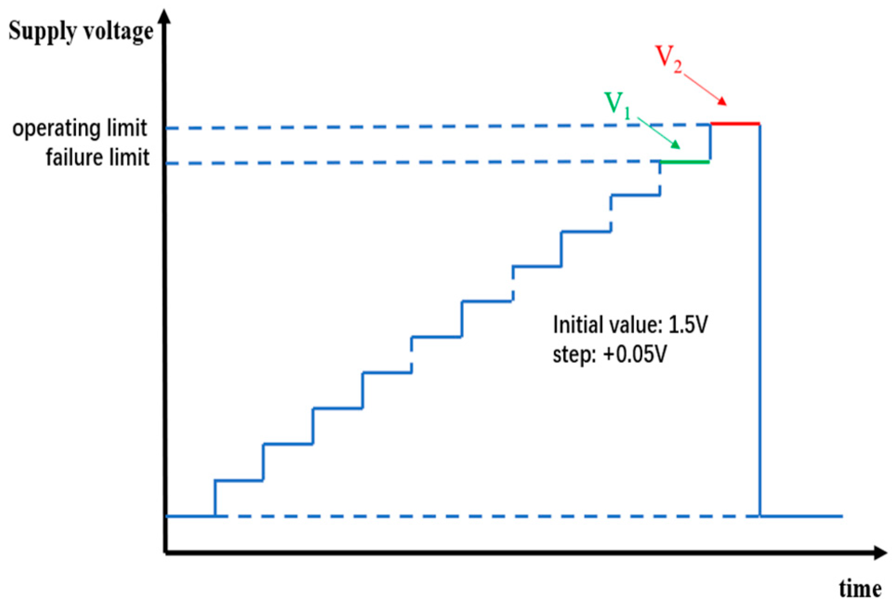
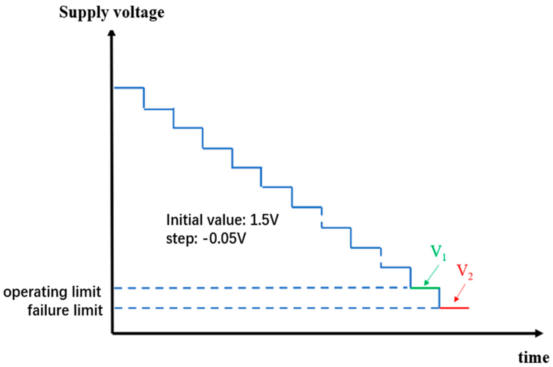
3.3.1. Power Supply Voltage Offset Limit Test for 3D-Packaged Memory
3.3.2. Input Clock Frequency Limit Test for 3D-Packaged Memory
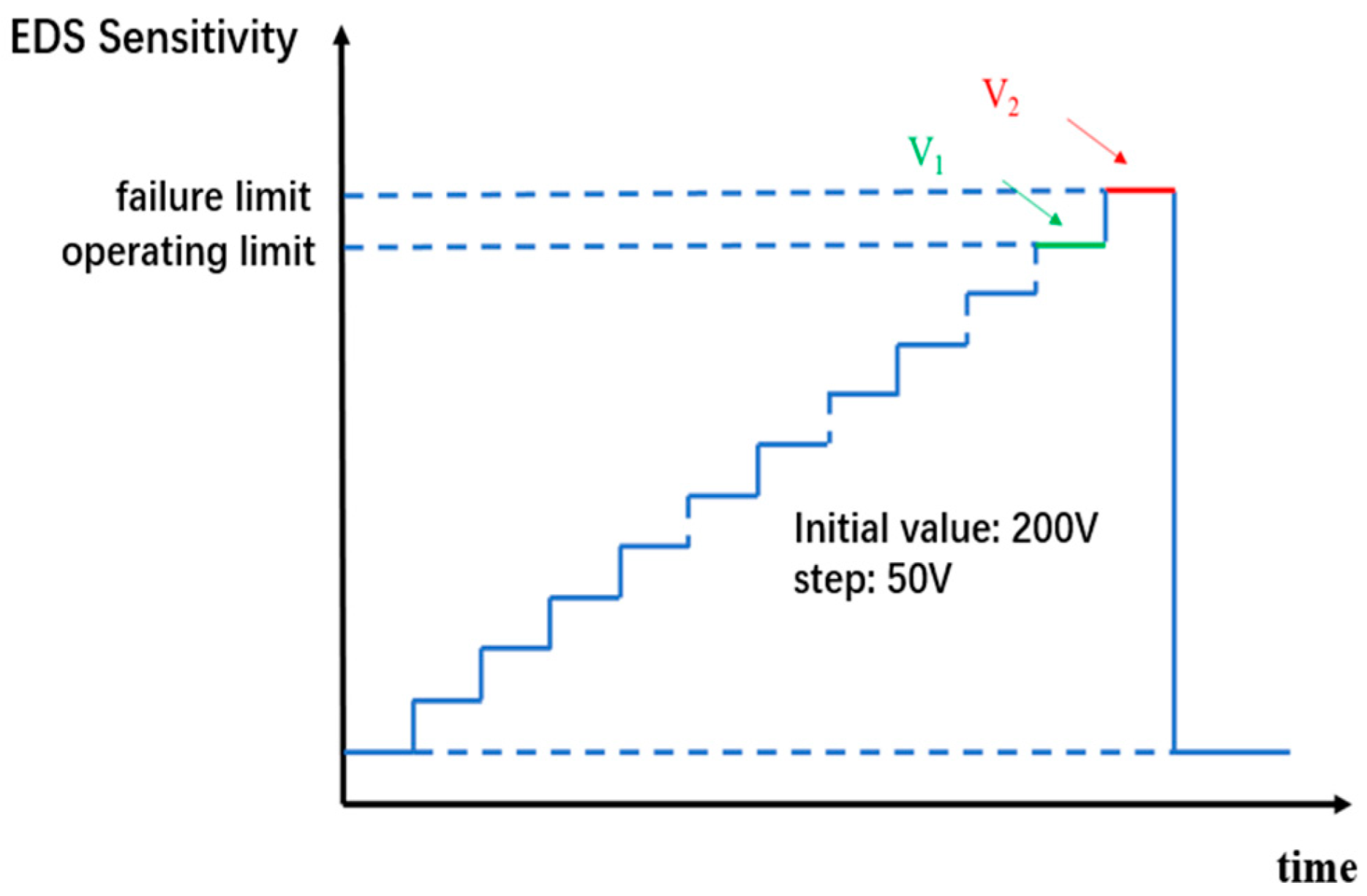
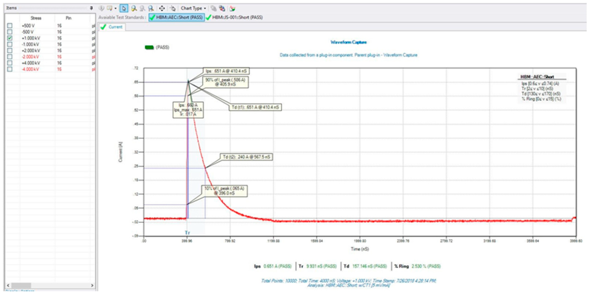
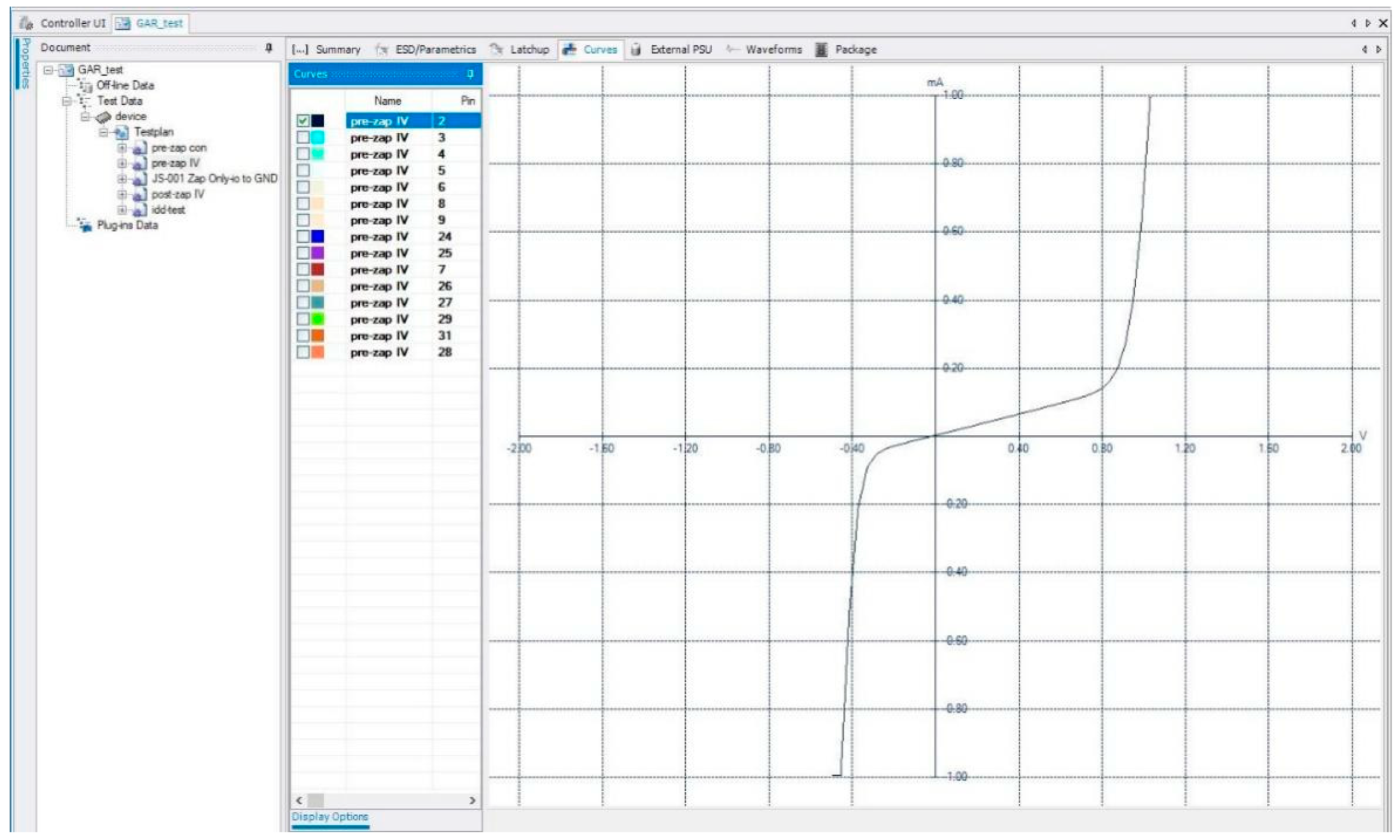
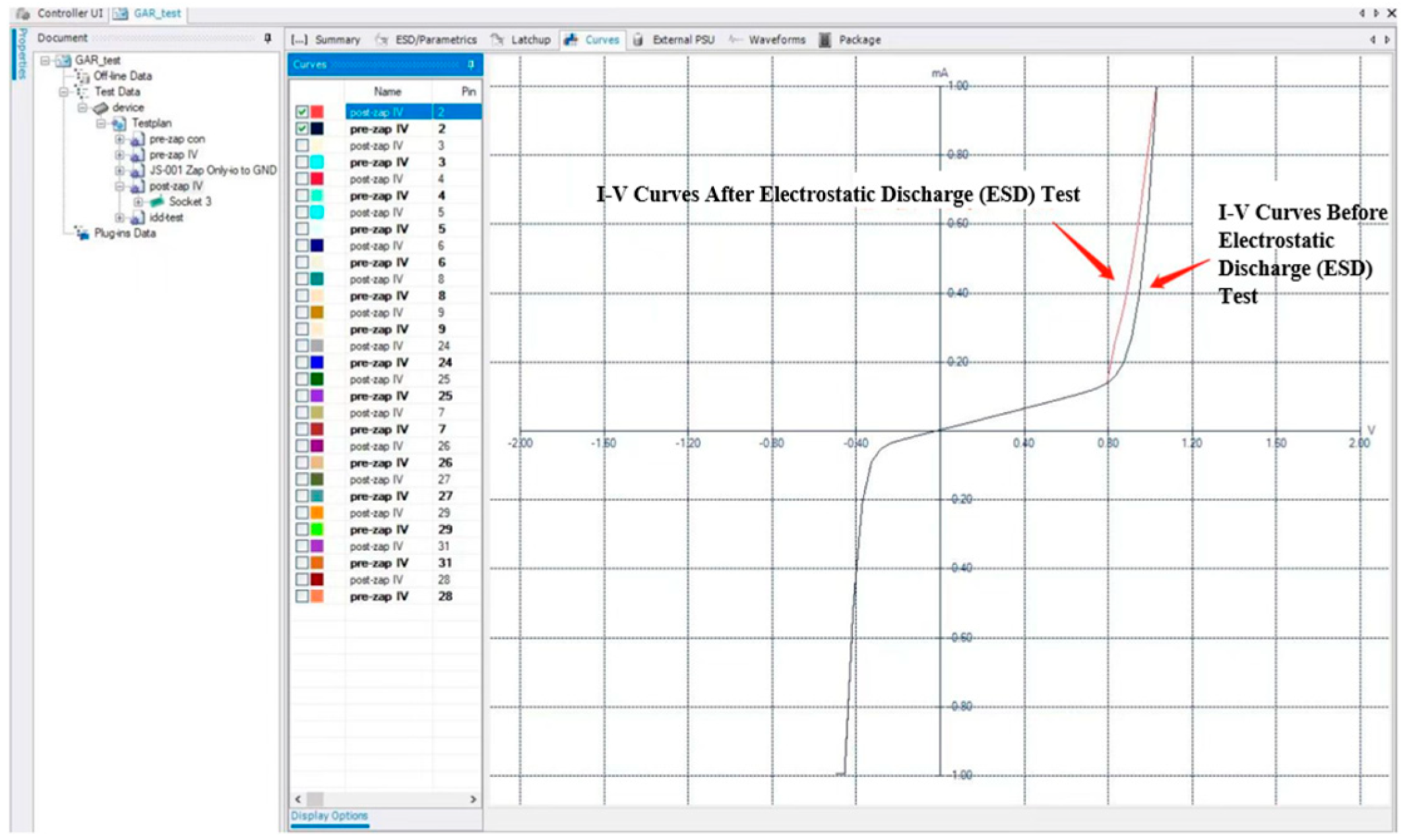
3.3.3. Electrostatic Discharge Sensitivity Limit Test for 3D-Packaged Memory
Electrostatic Discharge Sensitivity Test Procedure
Construction of Electrostatic Discharge Sensitivity Test Platform and PCB Design
3.4. Electrical Durability Limit Test for 3D-Packaged Memory
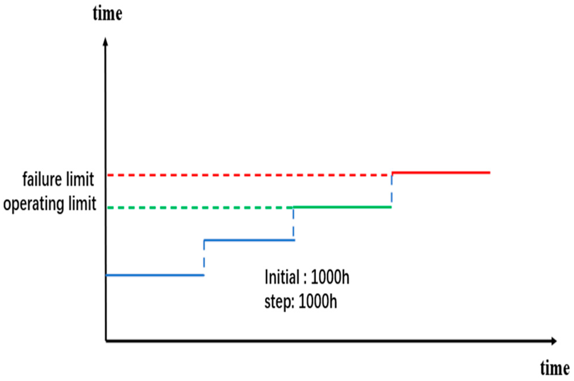
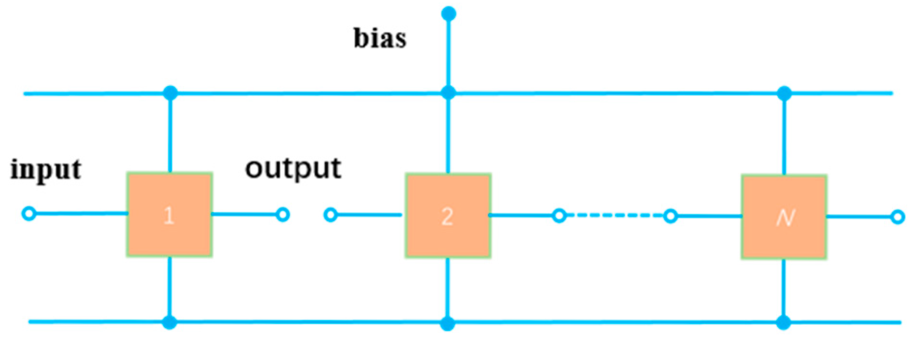
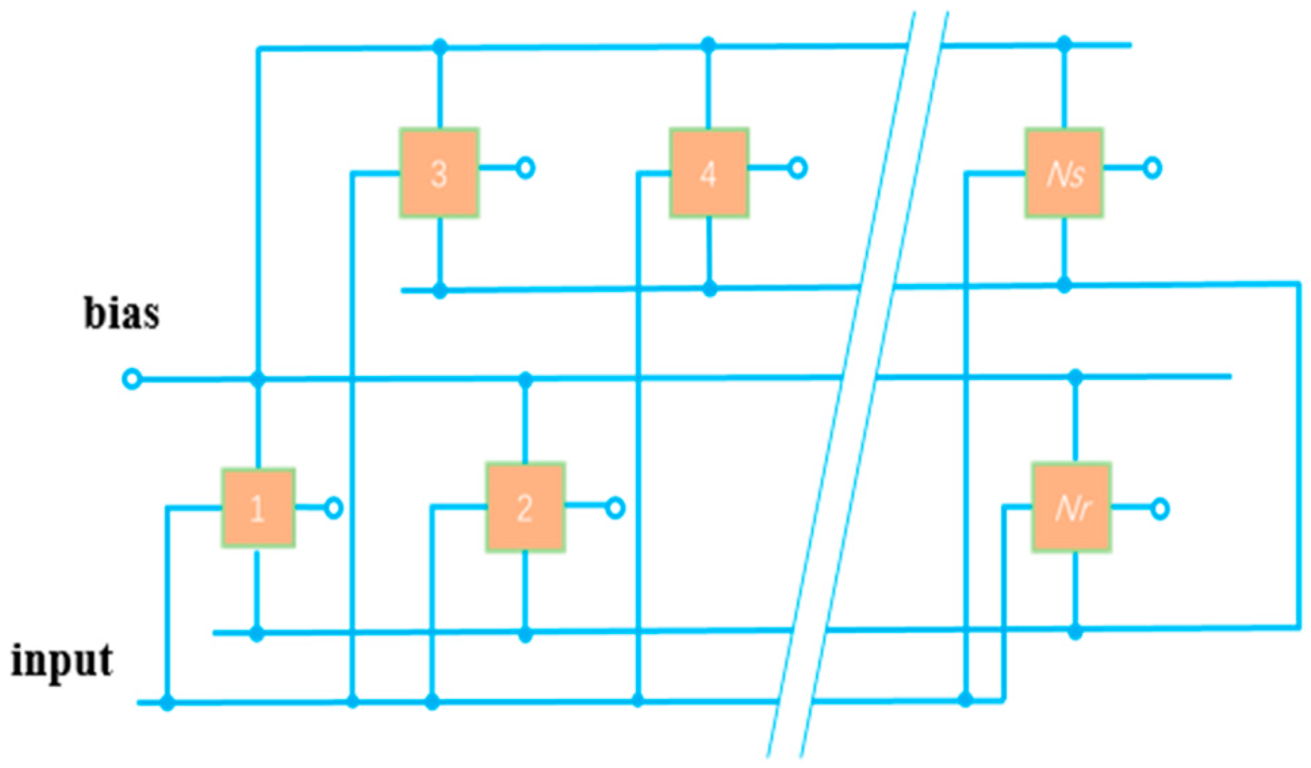
3.4.1. Principle of the Electrical Durability Test
3.4.2. Electrical Durability Test Procedure
- (1)
- Tests with a test temperature ≤ 150 °C
- (2)
- Tests with a test temperature ≥ 175 °C
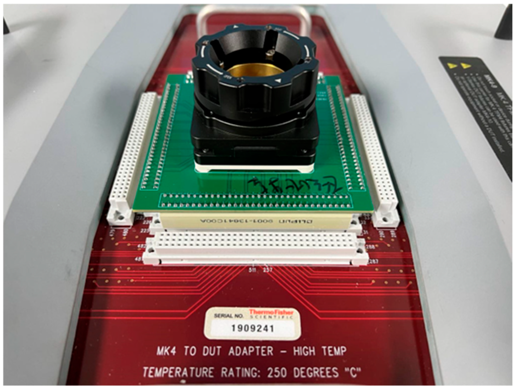
3.4.3. Construction of the Electrical Durability Test Platform and PCB Design
4. Test Results
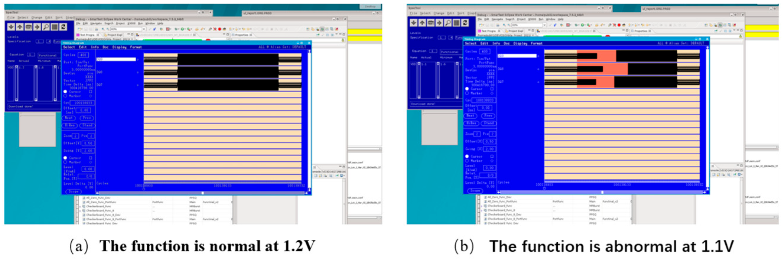
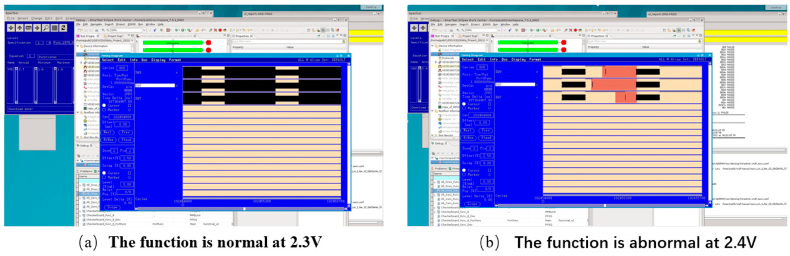
4.1. Test Results of the Power Supply Voltage Deviation Limit Test
4.2. Test Results of the Input Clock Frequency Limit Test
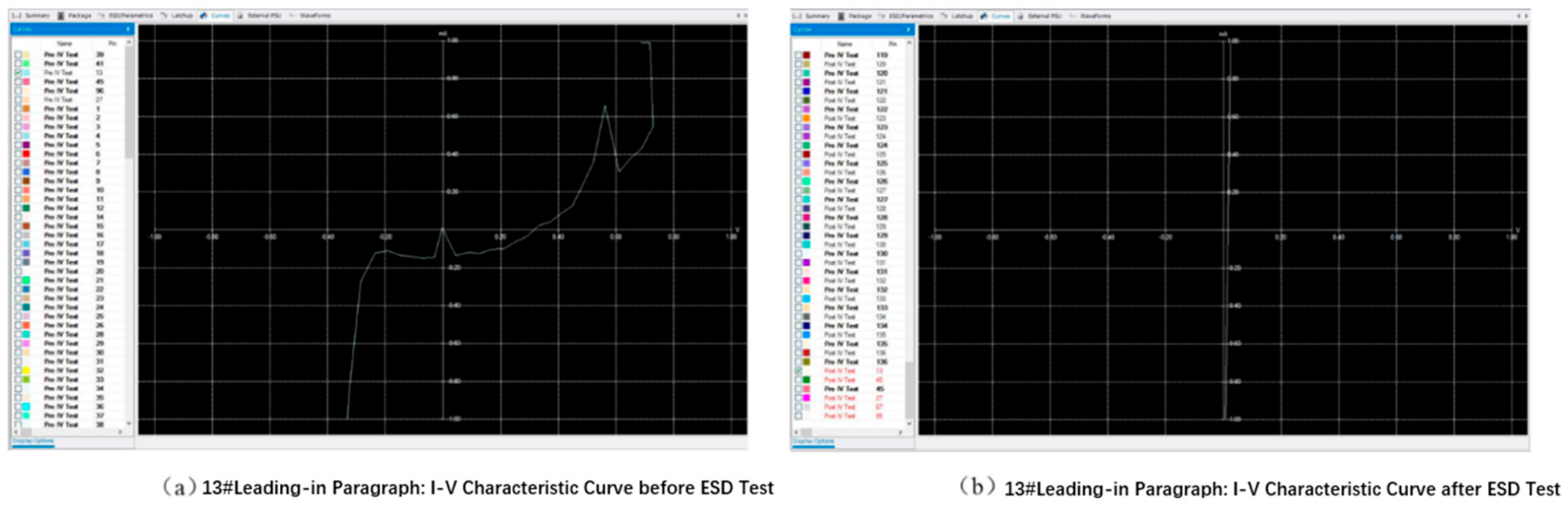
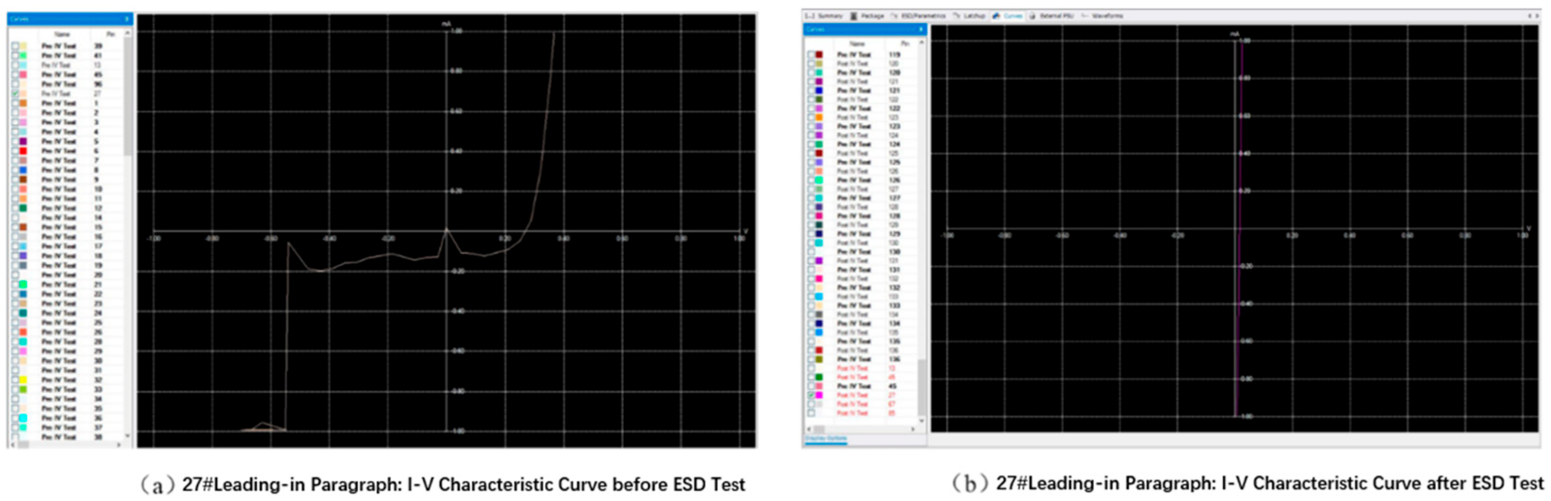
4.3. Analysis of the Test Results of the Electrostatic Discharge Sensitivity Limit Test
4.4. Analysis of the Test Results of the Electrical Durability Limit Test
5. Conclusions
Author Contributions
Funding
Data Availability Statement
Conflicts of Interest
References
- Zhou, S.; Ma, K.; Wu, Y.; Liu, P.; Hu, X.; Nie, G.; Ren, Y.; Qiu, B.; Cai, N.; Xu, S.; et al. Survey of Reliability Research on 3D Packaged Memory. Electronics 2023, 12, 2709. [Google Scholar] [CrossRef]
- Liu, M.F.; Zhou, Y.; Dai, J.; Qiao, Q.; Wang, J.; Chen, K. A novel 3D packaging technology for high-reliability applications. In Proceedings of the 2023 24th International Conference on Electronic Packaging Technology (ICEPT), Shihezi, China, 8 August 2023. [Google Scholar]
- Zhou, S.; Ma, K.; Wu, Y.; Liu, S.; Ma, C. Ultimate thermal stress reliability evaluation of 3D packaged memory. Microelectron. Reliab. 2025, 169, 115702. [Google Scholar] [CrossRef]
- Chen, Z.; Zhang, J.; Wang, S.; Wong, C.P. Challenges and prospects for advanced packaging. Fundam. Res. 2024, 4, 1455–1458. [Google Scholar] [CrossRef] [PubMed]
- Lancaster, A.; Keswani, M. Integrated circuit packaging review with an emphasis on 3D packaging. Integr. VLSI J. 2018, 60, 204–212. [Google Scholar] [CrossRef]
- Tunuguntla, S.P.; Yu, C.; Wang, D.; Karikalan, S. Performance evaluation of thermal interface material (TIM1) in FCBGA+HS package using Automatic Test Equipment (ATE) tester and package reliability tests. In Proceedings of the 2015 65th IEEE Electronic Components and Technology Conference (ECTC), San Diego, CA, USA, 26–29 May 2015; Institute of Electrical and Electronics Engineers Inc.: Piscataway, NJ, USA, 2015. [Google Scholar]
- BS EN IEC 60749-26; Semiconductor Devices—Mechanical and Climatic Test Methods Part 26: Electrostatic Discharge (ESD) Sensitivity Testing-Human Body Model (HBM). IEC: Geneva, Switzerland, 2024; pp. 1–51.
- Xia, M.; Wan, F.; Ravelo, B.; Zhang, Y.; Mei, G.; Liu, Y.; Chen, X. Charged Device Model ESD Sensitivity Tester Design and Application. IEEE Trans. Instrum. Meas. 2025, 74, 2001513. [Google Scholar] [CrossRef]
- Abessolo-Bidzo, D.; Smedes, T.; Huitsing, A.J. Predictive CDM simulation approach based on tester, package and full integrated circuit modeling. In Proceedings of the 2011 33rd Electrical Overstress/Electrostatic Discharge Symposium, EOS/ESD 2011, Anaheim, CA, USA, 11–16 September 2011; ESD Association: Anaheim, CA, USA, 2011. [Google Scholar]
- Rai, N.S.; Palecha, N.; Nagaraj, M. A brief overview of Test Solution Development for Semiconductor Testing. In Proceedings of the 2019 4th International Conference on Recent Trends on Electronics, Information, Communication & Technology (RTEICT), Bangalore, India, 17–18 May 2019; IEEE Computer Society: Washington, DC, USA, 2019; pp. 205–209. [Google Scholar]
- Lin, C.C. ESD Research of Integrated Circuits Under Harsh Environment. Bachelor’s Thesis, National Taiwan University, Taipei, China, 2023. [Google Scholar]
- Liu, Q.; Zhang, D.W. Auto-Trimming-Based Designs for the Test Optimization of Mass-Produced Automotive Microcontroller Unit Chip Probing Tests. Electronics 2024, 13, 4894. [Google Scholar] [CrossRef]
- Shin, T.; Han, J. A SCAN Chain Generator for Verification of Full-Custom Integrated Circuits. In Proceedings of the 18th International SoC Design Conference (ISOCC 2021), Jeju Island, Republic of Korea, 6 October 2021; IEEE: Piscataway, NJ, USA, 2021; pp. 335–336. [Google Scholar]
- Zhang, J.; Liu, Z.H.; Hu, X.; Liu, P.X.; Hu, Z.L.; Kuang, L.D. FATE: A Flexible FPGA-Based Automatic Test Equipment for Digital ICs. Electronics 2024, 13, 1667. [Google Scholar] [CrossRef]
- Cantoro, R.; Girard, P.; Masante, R.; Sartoni, S.; Reorda, M.S.; Virazel, A. Self-Test Libraries Analysis for Pipelined Processors Transition Fault Coverage Improvement. In Proceedings of the 2021 IEEE 27th International Symposium on On-Line Testing and Robust System Design (IOLTS), Torino, Italy, 28–30 June 2021; IEEE: Piscataway, NJ, USA, 2021. [Google Scholar]
- Kannan, K.T.; Vaisband, B.; Sahoo, K.; Iyer, S.S. An On-Chip ESD Sensor for Use in Advanced Packaging. IEEE Trans. Compon. Packag. Manuf. Technol. 2022, 12, 1051–1062. [Google Scholar] [CrossRef]
- Hristov, J.; Karadjova, V. On the p(x) approximation in the non-isothermal reaction kinetics by a generalized exponential integral the concept. Therm. Sci. 2021, 25, S321–S326. [Google Scholar] [CrossRef]
- Wang, X.N.; Su, X.B.; Yu, S.J.; Fang, Y.W. A Wiener-Arrhenius-Model-Based Method for Life Prediction of TWT Cathode. In Proceedings of the IVEC 2021: 2021 22nd International Vacuum Electronics Conference, Rotterdam, The Netherlands, 27 April 2021; IEEE: Piscataway, NJ, USA, 2021. [Google Scholar]
- You, J.X.; Fu, R.; Liang, H.M.; Lin, Y.G. A Non-Arrhenius Model for Mechanism Consistency Checking in Accelerated Degradation Tests. Actuators 2023, 12, 319. [Google Scholar] [CrossRef]


| No. | Test Item | Equipment | Typical Capabilities |
|---|---|---|---|
| 1 | Functional performance testing before and after stress testing | ATE Tester (Advantest Corporation, Penang, Malaysia) | Maximum channels: 1600; maximum digital transmission rate: 16 Gbps; maximum vector depth: 112 M; maximum scan chain depth: 28.5 G; edge placement accuracy (EPA): 75 ps; 64 independent power supplies; maximum current: 90 A; MTP test suite support; memory chip read/write testing speed: 8 Gbps; time measurement accuracy: 1 ps; high-end programmable logic devices (PLDs) with high-speed SerDes interfaces; testing speed: 25 Gb/s; output port rise/fall time: <20 ps |
| 2 | Power voltage limit testing | ||
| 3 | Input clock frequency limit testing |
| No. | Test Item | Equipment | Typical Capabilities |
|---|---|---|---|
| 1 | ESD Sensitivity Limit Testing | Multi-Pin ESD Sensitivity Tester (Sakai Denki Kogyo Co., Ltd. Sakai City, Japan) | Pin count: 1152 pin, 1728 pin, 2304 pin; HBM maximum test voltage: 8000 V; MM supported maximum test voltage: 2000 V |
| No. | Item | Specifications |
|---|---|---|
| 1 | Memory Architecture | 256 M × 72 bit |
| 2 | Nominal Voltage | 1.5 V ± 0.075 V |
| 3 | Maximum Clock Frequency | 667 MHz |
| 4 | Programmable Burst Length | 4, 8 |
| 5 | Package Type | BGA199 |
| Technical Parameter | Symbol | Basic Testing Conditions | Minimum Value | Maximum Value | Unit |
|---|---|---|---|---|---|
| Operating Current (1 Bank Activated–Precharged) | IDD0 | (VDD = 1.575 V and 1.283 V, VREF = 0.50 × VDD, VIH = VREF + 0.16 V, VIL = VREF − 0.16 V) | — | 375 | mA |
| Operating Current (1 Bank Activated–Read–Precharged) | IDD1 | — | 650 | mA | |
| Precharge Standby Current | IDD2N | — | 225 | mA | |
| Precharge Power-Down Current (Slow Exit Mode) | IDD2P0 | — | 90 | mA | |
| Precharge Power-Down Current (Fast Exit Mode) | IDD2P1 | — | 150 | mA | |
| Precharge Static Standby Current | IDD2Q | — | 225 | mA | |
| Activation Standby Current | IDD3N | — | 315 | mA | |
| Activation Power-Down Current | IDD3P | — | 215 | mA | |
| Burst Read Operating Current | IDD4R | — | 1000 | mA | |
| Burst Write Operating Current | IDD4W | — | 1100 | mA | |
| Burst Auto-Refresh Current | IDD5B | — | 1400 | mA | |
| Self-Refresh Current | IDD6 | — | 110 | mA | |
| Bank Interleaved Read Operating Current | IDD7 | — | 2000 | mA |
| Combination No. | Terminal A Connect Each Terminal to Terminal A in Sequence While Leaving Others Floating | Terminal B All Terminals of the Same Name Are Commonly Connected to Terminal B |
|---|---|---|
| 1 | All terminals except Vps1 | All Vps1 terminals |
| 2 | All input and output terminals | All other input and output terminals |
| Level | Voltage Range |
|---|---|
| Level 0 | <250 V |
| Level 1A | 250 V~499 V |
| Level 1B | 500 V~999 V |
| Level 1C | 1000 V~1999 V |
| Level 2 | 2000 V~3999 V |
| Level 3A | 4000 V~7999 V |
| Level 3B | ≥8000 V |
| Minimum Temperature TA (°C) | Shortest Time (h) | |||
|---|---|---|---|---|
| S Grade | B Grade | H Grade | K Grade | |
| 100 | - | - | 7500 | 7500 |
| 105 | - | - | 4500 | 4500 |
| 110 | - | - | 3000 | 3000 |
| 115 | - | - | 2000 | 2000 |
| 120 | - | - | 1500 | 1500 |
| 125 | 1000 | 1000 | 1000 | 1000 |
| 130 | 900 | 704 | 704 | - |
| 135 | 800 | 496 | 496 | - |
| 140 | 700 | 352 | 352 | - |
| 145 | 600 | 256 | 256 | - |
| 150 | 500 | 184 | 184 | - |
| 175 | - | 40 | - | - |
| 180 | - | 32 | - | - |
| 185 | - | 31 | - | - |
| ≥190 | - | 30 | - | - |
| Test Symbol | Test Conditions | Scope of Application |
|---|---|---|
| A | Steady-State, Reverse Bias Test | All kinds of linear circuits and digital circuits. Apply the specified reverse bias voltage to as many junctions as possible. |
| B | Steady-State, Forward Bias Test | All digital circuits and some linear circuits, for as many junctions as possible. |
| C | Steady-state, Power and Reverse Bias Test | Applicable to various digital circuits and some linear circuits whose input terminals can be reverse-biased and output terminals can be biased at the maximum power consumption state. |
| D | Parallel Excitation Test | Applicable to all kinds of circuits. During the test, all circuits must be applied with appropriate excitation signals to simulate the actual application as much as possible. Use the maximum external load, and the excitation frequency should not be lower than 50 Hz. |
| E | Ring Oscillator Test | Connect the output terminal of the last circuit to the input terminal of the first circuit. This series connection will generate free oscillation, and its frequency is determined by the transmission delay of each circuit and the relevant wiring, and the frequency ≥ 50 Hz. In the case where the circuit will cause inversion, an odd number of circuits should be used, and each circuit in the loop should be loaded with the rated maximum load. This condition provides an opportunity for continuous monitoring of fatal failures (i.e., loop blocking), so it cannot replace the intermediate test. |
| F | Temperature Acceleration Test | The device is biased under an ambient temperature (175 °C to 300 °C) far exceeding its highest rated temperature. At a higher temperature, the device usually cannot work normally. Therefore, special attention must be paid to selecting the bias circuit and conditions to ensure that the important current parts are properly biased and that no destructive overstress is generated on other parts of the circuit. |
| Sample Number | Absolute Maximum Rated Value Specified in the Detailed Specification | Operating Limit | Failure Limit |
|---|---|---|---|
| 1# | 1.425 V~1.575 V | 1.2 V~2.3 V | 1.1 V~2.4 V |
| Sample Number | Maximum Rated Value Specified in the Detailed Specification | Operating Limit | Failure Limit |
|---|---|---|---|
| 2# | 667 MHz | 667 MHz | 695 MHz |
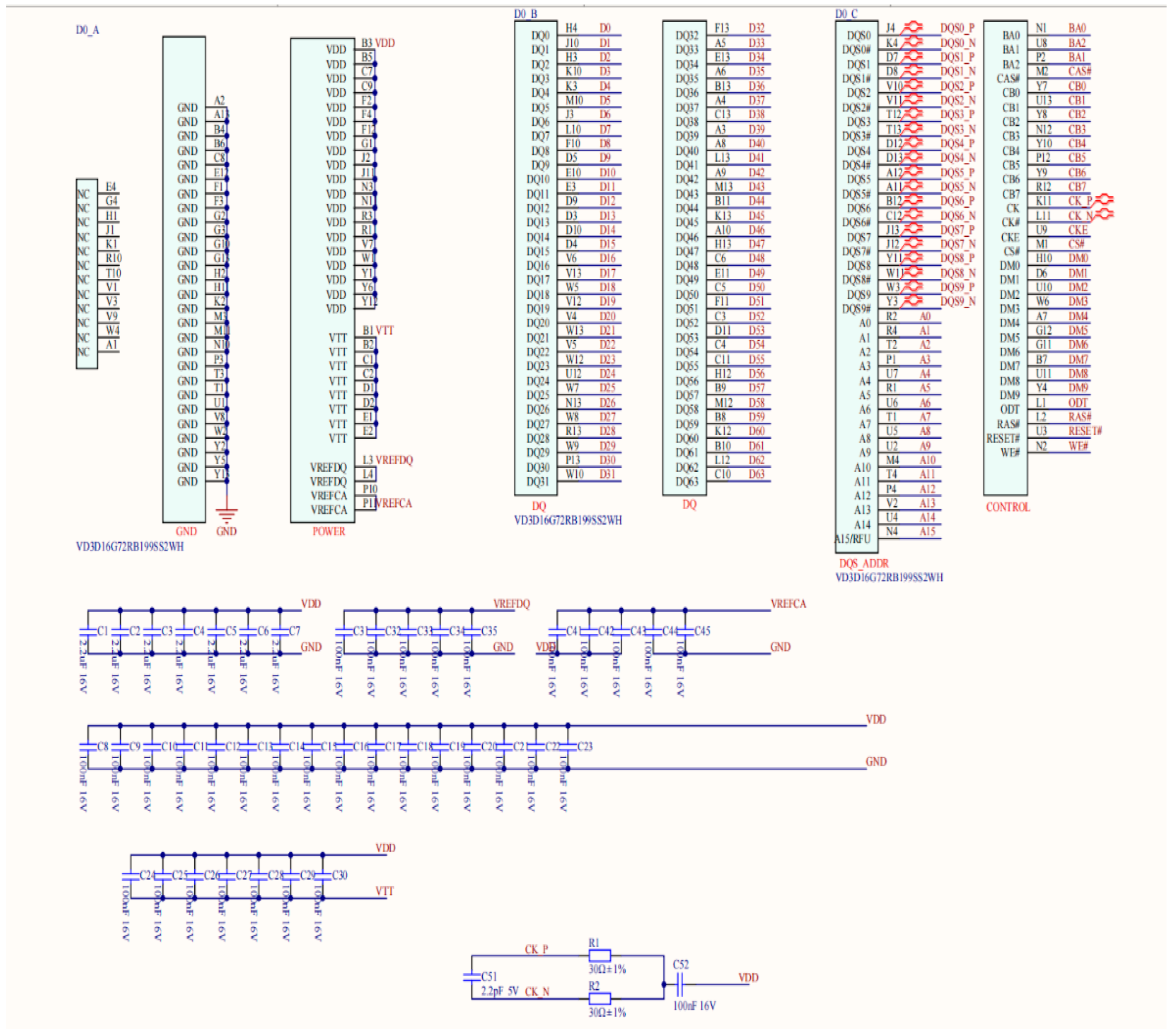
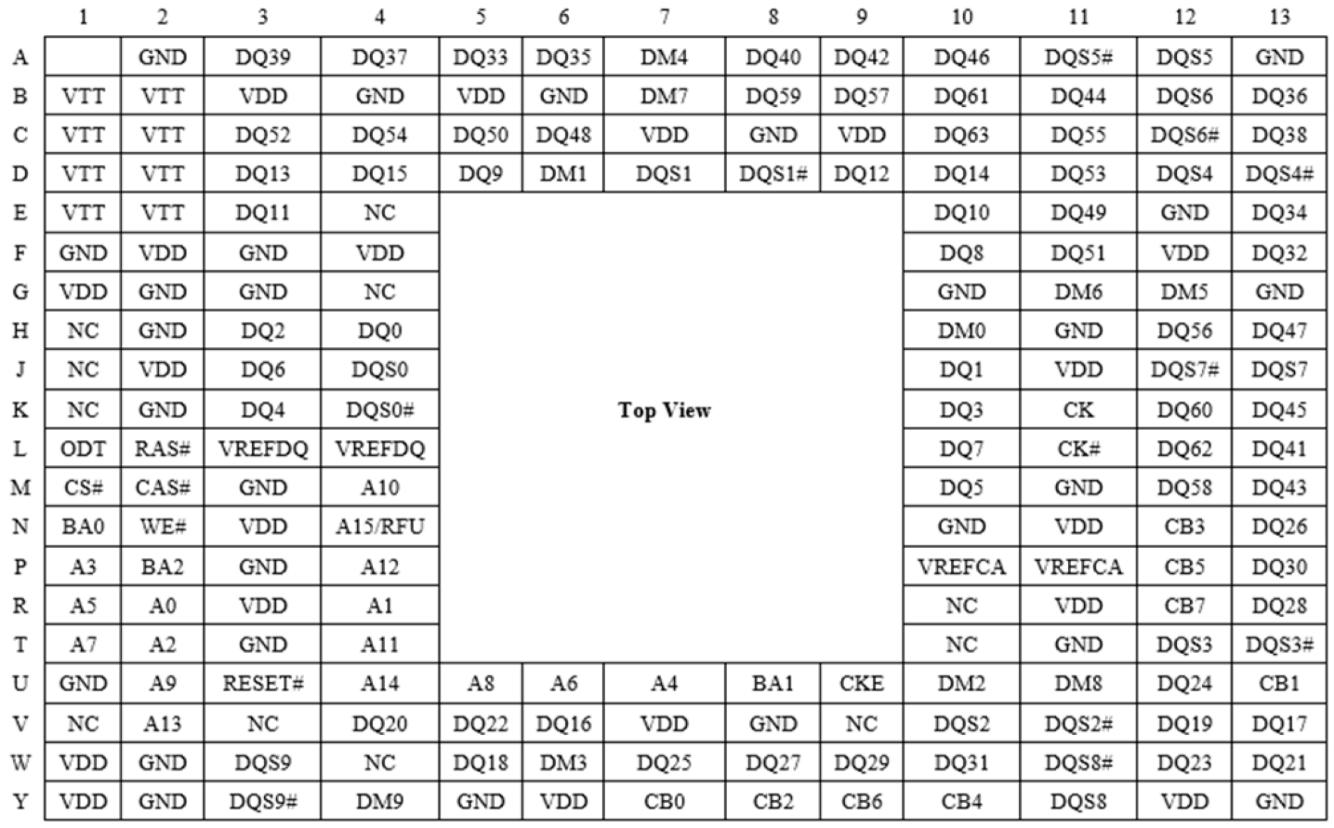
| Pin Name | Type | Function |
|---|---|---|
| A0~A14 | Input | 15-bit address input |
| A15/RFU | Input | A15/Reserved for future use pin |
| BA0~BA2 | Input | 3-bit Bank address input |
| A10/AP | Input | A10/Auto Precharge |
| A12/BC# | Input | A12/Burst Chop |
| CS# | Input | Chip Select Enable |
| RESET# | Input | Reset |
| CAS# | Input | CAS Command Input |
| RAS# | Input | RAS Command Input |
| WE# | Input | WE# Command Input |
| ODT | Input | On-Die Termination |
| CK,CK# | Input | Differential Clock Input |
| CKE | Input | Clock Enable Input |
| DM0~DM9 | Input | Data Mask |
| DQS0~DQS9, DQS0#~DQS9# | Input/Output | Data Strobe Input/Output |
| DQ0~DQ64 | Input/Output | Data Input/Output |
| CB0~CB7 | Input/Output | ECC Data Input/Output |
| VDD | Supply | Power Supply Voltage |
| GND | Supply | Ground |
| VREFDQ | Supply | Data Reference Voltage (0.5 × VDD) |
| VREFCA | Supply | Control, Command, and Address Reference Voltage (0.5 × VDD) |
| VTT | Supply | Termination Voltage (0.5 × VDD) |
| NC | Empty Lead |
| Sample Number | Rated Value Specified in the Detailed Specification | Operating Limit | Failure Limit |
|---|---|---|---|
| #3 | 2000 V | 3900 V | 4000 V |
| Serial Number | Parameter Name | Parameter Symbol | 4# | 5# | 6# | Unit |
|---|---|---|---|---|---|---|
| Measured Value | ||||||
| 1 | Operating Current (1 Bank Activated–Precharged) | IDD0 | 162 | 165 | 163 | mA |
| 2 | Operating Current (1 Bank Activated–Read–Precharged) | IDD1 | 249 | 252 | 250 | mA |
| 3 | Precharge Standby Current | IDD2N | 66 | 68 | 65 | mA |
| 4 | Precharge Power-down Current (Slow Exit Mode) | IDD2P0 | 16.3 | 16.5 | 15.9 | mA |
| 5 | Precharge Power-down Current (Fast Exit Mode) | IDD2P1 | 16.2 | 16.4 | 16.0 | mA |
| 6 | Precharge Static Standby Current | IDD2Q | 87 | 88 | 86 | mA |
| 7 | Activated Standby Current | IDD3N | 50 | 51.7 | 49 | mA |
| 8 | Activated Power-down Current | IDD3P | 16.3 | 16.5 | 16 | mA |
| 9 | Burst Read Operating Current | IDD4R | 353 | 354 | 350 | mA |
| 10 | Burst Write Operating Current | IDD4W | 355 | 355 | 345 | mA |
| 11 | Burst Auto-refresh Current | IDD5B | 393 | 401 | 397 | mA |
| 12 | Self-Refresh Current | IDD6 | 78 | 88 | 81 | mA |
| 13 | Bank Interleaved Read Operating Current | IDD7 | 545 | 556 | 554 | mA |
| 14 | Input Leakage Current | ILIL | −0.003 | −0.002 | −0.002 | μA |
| ILIH | 0.009 | 0.01 | 0.009 | μA | ||
| 15 | Output Leakage Current | ILOL | −0.003 | −0.002 | −0.002 | μA |
| ILOH | 0.009 | 0.01 | 0.009 | μA | ||
| 16 | DQS-DQ Delay | tDQSQ | 26 | 35 | 23 | ps |
| 17 | Function | Qualified | Qualified | Qualified | / | |
| Serial Number | Parameter Name | Parameter Symbol | 4# | 5# | 6# | Unit |
|---|---|---|---|---|---|---|
| Measured Value | ||||||
| 1 | Operating Current (1 Bank Activated–Precharged) | IDD0 | 165 | 163 | 162 | mA |
| 2 | Operating Current (1 Bank Activated–Read–Precharged) | IDD1 | 253 | 251 | 250 | mA |
| 3 | Precharge Standby Current | IDD2N | 68 | 68 | 66 | mA |
| 4 | Precharge Power-Down Current (Slow Exit Mode) | IDD2P0 | 16.5 | 16.8 | 16.3 | mA |
| 5 | Precharge Power-down Current (Fast Exit Mode) | IDD2P1 | 16.4 | 16.4 | 16.2 | mA |
| 6 | Precharge Static Standby Current | IDD2Q | 88 | 88 | 87 | mA |
| 7 | Activated Standby Current | IDD3N | 51 | 51.7 | 50 | mA |
| 8 | Activated Power-Down Current | IDD3P | 16.5 | 16.9 | 16.2 | mA |
| 9 | Burst Read Operating Current | IDD4R | 354 | 349 | 354 | mA |
| 10 | Burst Write Operating Current | IDD4W | 347 | 350 | 353 | mA |
| 11 | Burst Auto-Refresh Current | IDD5B | 402 | 399 | 393 | mA |
| 12 | Self-Refresh Current | IDD6 | 83 | 79 | 78 | mA |
| 13 | Bank Interleaved Read Operating Current | IDD7 | 555 | 551 | 545 | mA |
| 14 | Input Leakage Current | ILIL ILIH | −0.002 0.009 | −0.004 0.009 | −0.003 0.009 | μA μA |
| 15 | Output Leakage Current | ILOL ILOH | −0.002 0.009 | −0.004 0.009 | −0.003 0.009 | μA μA |
| 16 | DQS-DQ Delay | tDQSQ | 45 | 21 | 37 | ps |
| 17 | Function | Qualified | Qualified | Qualified | / | |
| Sample Number | Electrical Durability Test Time Specified in the Detailed Specification | Operating Limit (Constant Stress with Timed End) |
|---|---|---|
| #4~#6 | 1000 h | 2000 h |
Disclaimer/Publisher’s Note: The statements, opinions and data contained in all publications are solely those of the individual author(s) and contributor(s) and not of MDPI and/or the editor(s). MDPI and/or the editor(s) disclaim responsibility for any injury to people or property resulting from any ideas, methods, instructions or products referred to in the content. |
© 2025 by the authors. Licensee MDPI, Basel, Switzerland. This article is an open access article distributed under the terms and conditions of the Creative Commons Attribution (CC BY) license (https://creativecommons.org/licenses/by/4.0/).
Share and Cite
Zhou, S.; Ma, K.; Cai, Z.; Liu, S.; Xiang, J.; Ma, C. Research on the Evaluation Method of Electrical Stress Limit Capability Based on Reliability Enhancement Theory. Electronics 2025, 14, 3056. https://doi.org/10.3390/electronics14153056
Zhou S, Ma K, Cai Z, Liu S, Xiang J, Ma C. Research on the Evaluation Method of Electrical Stress Limit Capability Based on Reliability Enhancement Theory. Electronics. 2025; 14(15):3056. https://doi.org/10.3390/electronics14153056
Chicago/Turabian StyleZhou, Shuai, Kaixue Ma, Zhihua Cai, Shoufu Liu, Jian Xiang, and Chi Ma. 2025. "Research on the Evaluation Method of Electrical Stress Limit Capability Based on Reliability Enhancement Theory" Electronics 14, no. 15: 3056. https://doi.org/10.3390/electronics14153056
APA StyleZhou, S., Ma, K., Cai, Z., Liu, S., Xiang, J., & Ma, C. (2025). Research on the Evaluation Method of Electrical Stress Limit Capability Based on Reliability Enhancement Theory. Electronics, 14(15), 3056. https://doi.org/10.3390/electronics14153056