Article

A High-Efficiency GaN-on-Si Power Amplifier Using a Rapid Dual-Objective Optimization Method for 5G FR2 Applications

School of Electronics and Communication Engineering, Guangzhou University, Guangzhou 510006, China
*
Author to whom correspondence should be addressed.
Electronics 2025, 14(15), 2996; https://doi.org/10.3390/electronics14152996
Submission received: 11 July 2025 / Revised: 19 July 2025 / Accepted: 24 July 2025 / Published: 27 July 2025
(This article belongs to the Special Issue Advanced RF/Microwave Circuits and System for New Applications)

Abstract

A broadband, efficient monolithic microwave integrated circuit power amplifier (MMIC PA) in OMMIC’s 0.1 μm GaN-on-Si technology for 5G millimeter-wave communication is presented. This study concentrates on the output matching design, which has an important influence on the PA’s performance. A compact one-order synthesized transformer network (STN) is adopted to match the 50 Ω load to the extracted large-signal output model of the transistor. A dual-objective strategy is developed for parameter optimization, incorporating the impedance transformation trajectory inside the predefined optimal impedance domain (OID) that satisfies the required specifications, with approximation to selected optimal load impedances. By introducing a custom adjustment factor β into the error function, coupled with an automated iterative tuning process based on S-parameter simulations, desired broadband matching results can be rapidly achieved. The proposed two-stage PA occupies a small chip area of only 1.23 mm2 and demonstrates good frequency consistency over the 24–31 GHz band. Continuous-wave characterization shows a flat small-signal gain of 19.7 ± 0.5 dB; both the output power (Pout) and the power-added efficiency (PAE) at the 4 dB compression point remain smooth, ranging from 32.3 to 32.7 dBm and 35.5% to 37.8%, respectively. The peak PAE reaches up to nearly 40% at the center frequency.

1. Introduction

5G has been extensively deployed worldwide and serves as fundamental infrastructure for digital transformation. It has now evolved into 5G-Advanced (5G-A), corresponding to Release 18 of the 3GPP technical specifications. Beyond ongoing network performance upgrades, Release 18 emphasizes further integration of the 5G ecosystem with non-terrestrial networks, aiming to achieve ubiquitous global cellular connectivity [1]. With growing adoption of the broadband internet services provided by commercial low-Earth-orbit (LEO) satellite constellations like Starlink and OneWeb, the convergence of satellite and terrestrial 5G networks is emerging as a significant trend that will play a crucial role in future space–air–ground integrated networks [2].
As a cornerstone of 5G-A and high-throughput satellite communication (SATCOM), millimeter-wave (mmWave) technology shows great promise for cutting-edge fields, owing to its distinctive features of a wide contiguous bandwidth, low latency, flexible deployment, and high-precision sensing. The 5G New Radio mmWave spectrum, known as Frequency Range 2 (FR2), extends from 24.25 GHz up to 71 GHz, covering the K to V bands. Despite its many benefits, mmWave technology faces high-frequency-related problems, including severe path, penetration, and blockage losses [3]. Moreover, modern wireless systems impose stringent requirements on size, weight, power, and cost (SWaP-C), creating considerable challenges for designing mmWave front-end modules [4,5], particularly the power amplifier (PA), which directly affects signal quality, coverage, and energy consumption. Therefore, to address the ever-growing demand for data, support multiple communication standards, and ensure a high-quality user experience, the development of efficient mmWave PAs with a small footprint and a watt-level output power (Pout) over a wide bandwidth has become a key research focus.
The performance bottleneck for PAs is essentially dictated by the device technology. As a leading third-generation wide-bandgap semiconductor, gallium nitride (GaN) offers outstanding properties, including a high breakdown electric field, high saturation velocity, and good thermal conductivity. These inherent advantages enable GaN high-electron-mobility transistors (HEMTs) to achieve a better frequency response, operate at higher bias voltages, and sustain greater power densities [6]. Compared to silicon-based processes such as CMOS and SOI, which typically require transistor stacking to increase the voltage swing under the same current conditions [7,8], or gallium arsenide (GaAs) counterparts, which rely on bulky and lossy power-combining networks to attain comparable Pout [9,10], the adoption of GaN devices simplifies the circuit design and eases thermal management. These features make GaN PAs ideal for mmWave communication systems that demand compact, lightweight, and high-efficiency solutions [6,11,12,13,14,15,16].
In addition to device-level considerations, the pursuit of both broadband operation and high efficiency in PAs necessitates careful circuit design. Nevertheless, these two goals are often mutually restrictive. Ensuring broadband impedance matching and a flat frequency response may result in reduced efficiency over part of or even the entire operating band, whereas optimizing the matching network (MN) for peak efficiency at specific frequencies inevitably sacrifices bandwidth. Numerous studies have illustrated this inherent contradiction. For instance, distributed amplifiers utilize artificial transmission lines to absorb the parasitic capacitance of transistors, enabling a multi-octave bandwidth but at the expense of low gain, poor power-added efficiency (PAE), and large chip area [17]. Balanced amplifiers leverage a pair of quadrature couplers to cancel the reflections caused by mismatches at the circuit’s input and output, thereby achieving an excellent broadband voltage standing wave ratio and stability, but they also incur a higher insertion loss, which degrades the PAE [5]. Others, comprising switch-mode PAs (Class E, F, F−1, etc.) that rely on harmonic control or waveform shaping to minimize the overlap between the output voltage and current [18,19], as well as Doherty PAs that use a load modulation technique, have also been extensively researched [20]. Overall, taking all of the necessary trade-offs into account, the most cost-effective solution lies in the design and optimization of the MN. One category relates to a CAD-dependent numerical optimization methodology, with the simplified real-frequency technique (SRFT) as a notable example. The SRFT enables the construction of a broadband MN by optimizing the transducer power gain function based on acquired load data, without predefining any topology [21]. However, a robust and computationally expensive optimization algorithm ought to be employed in order to obtain the globally optimal solution. Another category belongs to mathematically synthesized networks derived from broadband matching theory [22,23,24]. While these approaches are straightforward to implement, they are constrained by the equivalent circuit model of the load, generate MNs with fixed or patterned topologies, and require the bandwidth, impedance transformation ratio (ITR), and ripple of the frequency response to be balanced during the design procedure [18,19,25].
This paper presents a 0.1 μm GaN-on-Si MMIC PA designed through a combination of analytical network synthesis and numerical optimization methods. Special attention is given to the output matching network (OMN), which employs a synthesized transformer network to absorb the transistor’s output capacitance (Cout). A simple method is offered for selecting the optimal load impedance (Zopt) that enables a favorable compromise between Pout and PAE. Furthermore, a dual-objective optimization strategy guided by impedance rather than performance metrics is developed, along with an error function incorporating a tunable factor β to manage matching quality across different frequencies. The proposed parameter optimization procedure operates efficiently, as it avoids the need for time-consuming harmonic balance (HB) simulations. The implemented two-stage PA exhibits consistent small- and large-signal characteristics across the 24–31 GHz band. The electromagnetic (EM) simulation outcomes are summarized and benchmarked against those from recent work.

2. A Rapid Output Matching Optimization Method with Dual-Objective Orientation

As the final stage of RF power transmission in a PA, the OMN plays a decisive role. The large-signal behavior of a transistor is sensitive to the load impedance, making precise OMN design essential to achieving the expected matching conditions. At mmWave frequencies, Zopt shows pronounced frequency dependence due to the device’s enhanced parasitic effects, primarily the nonlinear drain-source capacitance (Cds), and is denoted as Zopt(fi) at the frequency fi. Additionally, the OMN transforms the standard 50 Ω load into the impedance Zomn(fi), whose rotational trajectory on the Smith chart opposes that of Zopt(fi). These two issues hinder the design of a broadband OMN, making point-by-point matching unfeasible, especially under complexity limitations. Thus, industry practice is to choose an appropriate OMN topology and fine-tune its component values to closely approach Zopt(fi) with reasonable compromises in matching accuracy. This section details a rapid and automated parameter optimization method for the OMN, free of artificial intelligence algorithms.

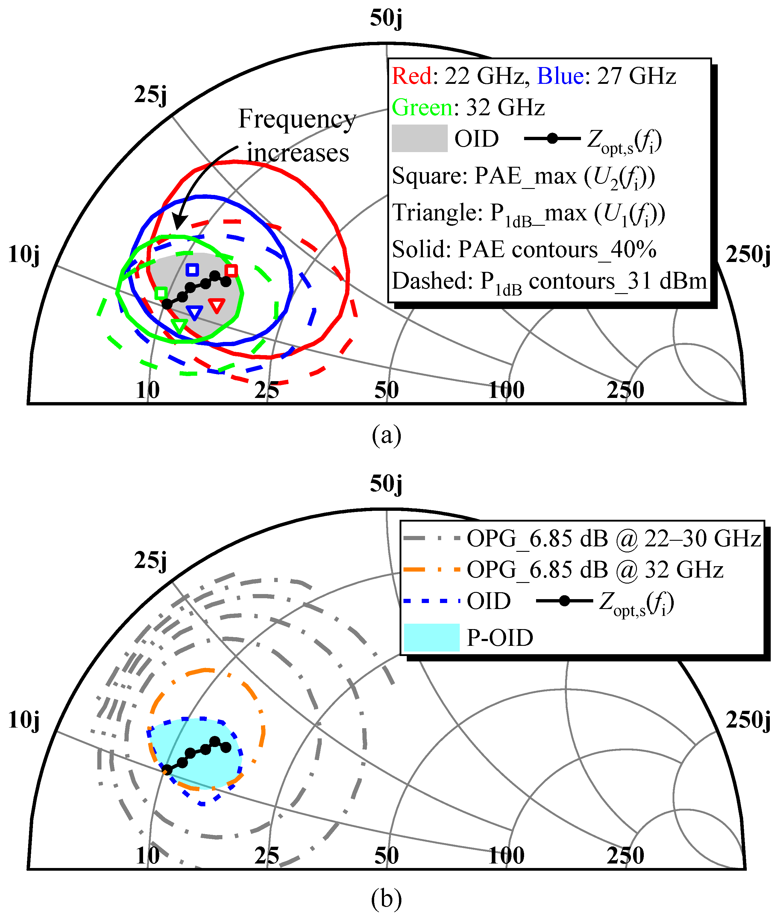
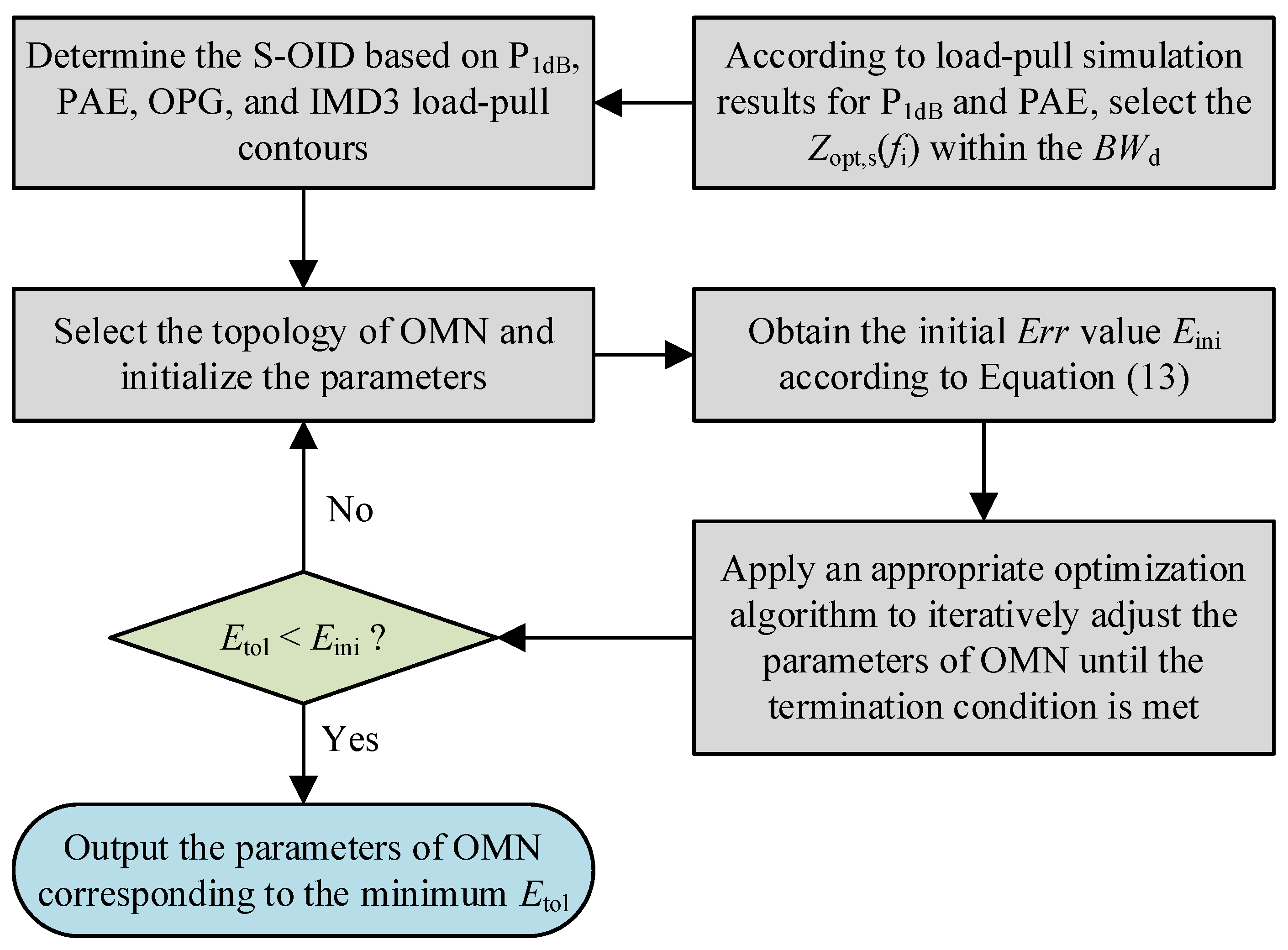
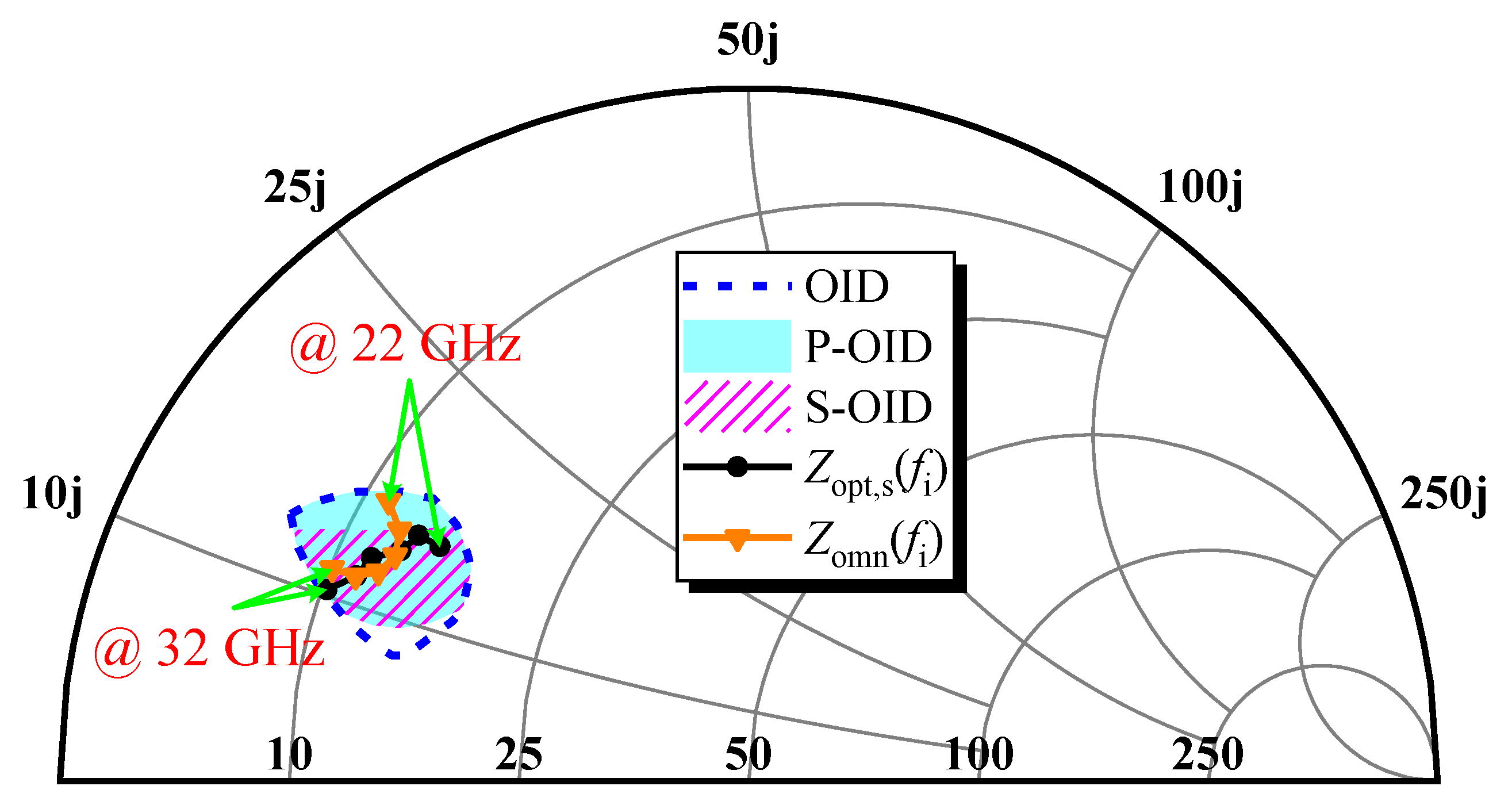
2.1. Selection of the Optimal Load Impedance

The intended operating bandwidth (BWo) is 24–30 GHz. To account for possible performance deviations due to process variations and inaccuracies in device modeling, the design bandwidth (BWd) is defined by adding a 2 GHz margin to both the lower and upper boundaries of BWo, thus providing sufficient frequency redundancy.
To guarantee the linear output capability of the PA, load-pull simulations were conducted on a stabilized 46 × 8 μm power cell at the 1 dB compression point at six frequencies fi (i = 1 to 6) spaced 2 GHz apart in the BWd of 22–32 GHz. The obtained Zopt(fi) for the maximum P1dB and PAE are denoted as U1(fi) and U2(fi), respectively, both of which are expressed in the complex impedance form, as given by Equations (1) and (2). Varying degrees of deviation between U1(fi) and U2(fi) exist at different frequencies. Selecting a target matching impedance Zopt,s(fi) closer to U1(fi) favors a higher P1dB but moves further away from U2(fi), resulting in a reduced PAE. Consequently, Zopt,s(fi) is generally chosen at an intermediate position between U1(fi) and U2(fi) to strike a balance between P1dB and PAE. To determine Zopt,s(fi), weighting coefficients m and n are assigned to the impedance points U1(fi) and U2 (fi), respectively, with m + n = 1, as described by Equation (3). Since PAE exhibits greater fluctuations in response to mismatch than P1dB, m and n are set to 1/3 and 2/3, respectively. The calculated values are listed in Table 1 and plotted in Figure 1a.
U 1 f i = R 1 f i + j X 1 f i
U 2 f i = R 2 f i + j X 2 f i
Z opt , s f i = m U 1 f i + n U 2 f i = m R 1 f i + n R 2 f i + j m X 1 f i + n X 2 f i

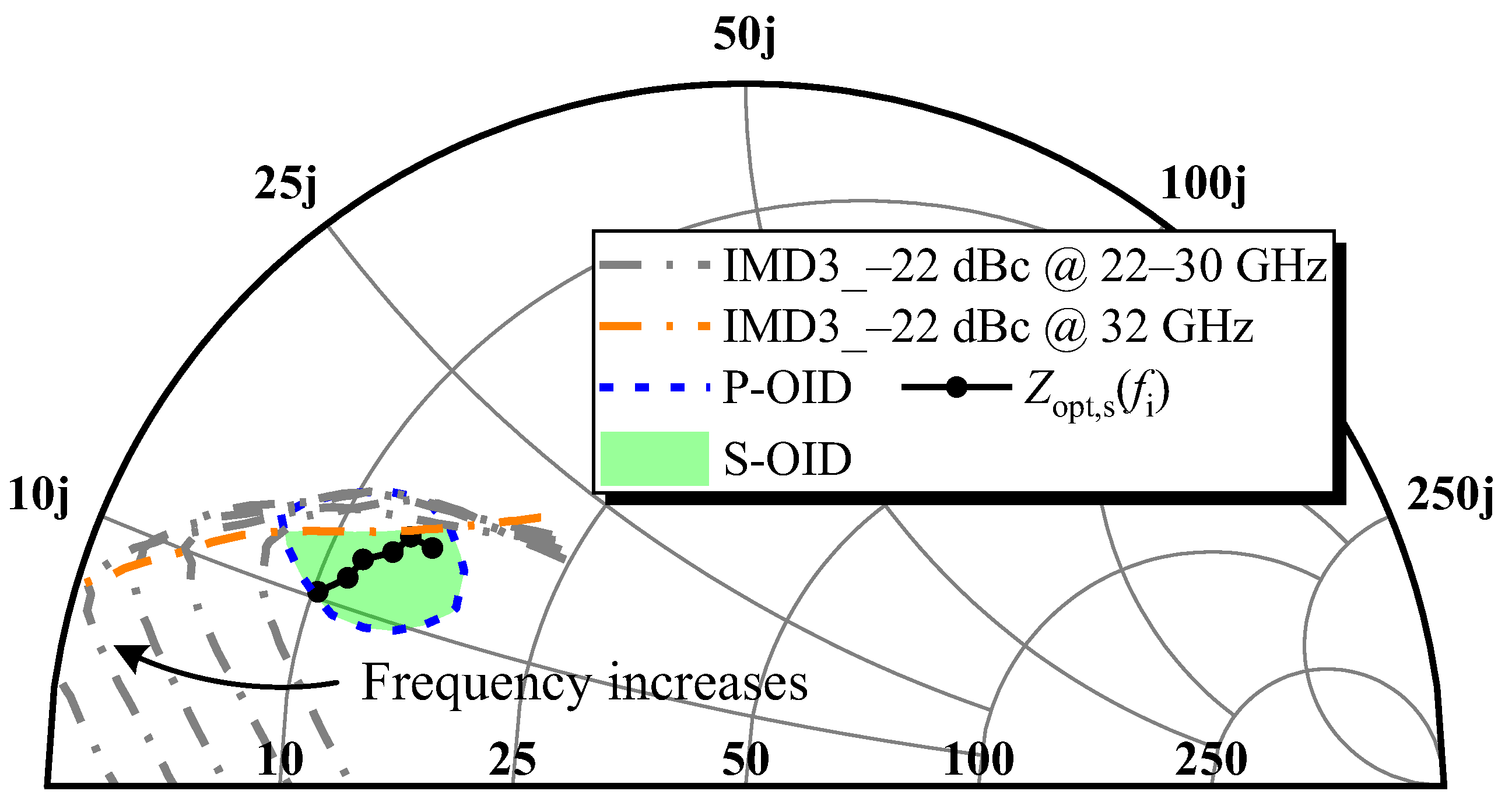
2.2. Determination of the Optimal Impedance Domain

Subsequently, the optimal impedance domain (OID) is defined as the intersection region of the P1dB contour of 31 dBm and the PAE contour of 40%, as highlighted by the gray shading in Figure 1a. With an increasing frequency, the P1dB and PAE contours gradually shrink, and both rotate counterclockwise toward the real axis of the Smith chart, reflecting the trajectory of Zopt(fi). This trend indicates that the transistor’s performance deteriorates at higher frequencies. Approximately two-thirds of the OID boundary is delineated by the contours at 32 GHz. The operating power gain (OPG) is also a key metric that should not be overlooked, as achieving the target gain with fewer amplification stages can greatly improve the overall PAE. As depicted in Figure 1b, a value of 6.85 dB is chosen for the OPG because the corresponding narrowest contour at 32 GHz and the OID together create a new overlap area that still contains every Zopt,s(fi), without significantly reducing the original OID, which is termed the preferred OID (P-OID). As long as all Zomn(fi) across BWd fall inside the P-OID, the transistor’s large-signal output capability is assured, eliminating lengthy HB simulations. The OMN parameter optimization can then be focused on minimizing the offset between each Zomn(fi) and Zopt,s(fi).
When the transistor enters the gain compression region, its transconductance gm and Cds exhibit strong nonlinearity. Therefore, based on the derived P-OID, two-tone load-pull simulations can be further performed to obtain the third-order intermodulation distortion (IMD3) contours, leading to a stricter definition of the OID and thus providing more comprehensive guidance for optimizing the parameters of the OMN. IMD3 is a major concern in linearity requirements because it lies near the operating frequencies and causes spectral regrowth. Assume that the two-tone excitation vin (t) is expressed as
v in t = A cos ω 1 t + B cos ω 2 t
where A and B represent the amplitudes of two fundamental components. Neglecting memory effects and higher-order nonlinearities, the drain current equations for IMD3 frequencies are
I d = I d 0 + k = 1 n g m k V gs k
i 2 ω 1 ω 2 = 3 4 g m 3 A 2 B cos 2 ω 1 ω 2 t
i 2 ω 2 ω 1 = 3 4 g m 3 A B 2 cos 2 ω 2 ω 1 t
where Id and Id0 represent the total drain current and the DC drain current, respectively, while Vgs denotes the RF voltage applied across the gate-source terminals. The parameter k indicates the nonlinear order, and gmk is the k-th order transconductance. For every frequency component present at the device ports, gmk values are associated with the load impedance, as they are defined by the combinations of the drain and gate voltages with the current during an RF swing [26]. Since gm3 is determined by the IMD3 products shown in Equations (6) and (7), the IMD3 value is also related to the load impedance [27]. Figure 2 depicts the IMD3 load-pull contours for a two-tone sinusoidal signal with a power level around the 1 dB compression point, a center frequency of fi, and a 100 MHz tone spacing. As can be observed, the contours enclose a relatively wide impedance domain that extends into the lower half of the Smith chart and shifts toward the short-circuit point as the frequency increases. The IMD3 contour of −22 dBc at 32 GHz passes through Zopt,s(fi) with the maximum imaginary part, overlapping with the previously identified P-OID to form a strict OID (S-OID) constrained by four performance metrics.
Importantly, although the OID is progressively reduced by an increasing number of constraints, it is purposely maintained to encompass all Zopt,s(fi) to ensure the consistency and compatibility of the optimization objectives.

2.3. Verification of the Impedance Point Within the OID

The OID is essentially a closed polygon formed by connecting a series of discrete impedance points successively. To quickly determine whether the complex impedance Zomn(fi) resides inside the predefined OID, the ray-casting algorithm is utilized, as it is well suited to both convex and concave polygons and offers high computational efficiency. It works by emitting a ray from the point of interest and counting the intersections with the polygon boundaries, applying the parity rule to distinguish between interior and exterior positions. Consider the OID as a non-self-intersecting closed polygon with V vertices on the real (X)–imaginary (Y) plane, with the vertex coordinates {(x1, y1), (x2, y2), …, (xV, yV)}, where x1 = xV and y1 = yV to ensure closure. The point under investigation, Zomn(fi), has the coordinates (xomn, yomn). To facilitate computation, the ray is emitted horizontally towards the positive X-axis. The specific identification steps are as follows:
Step 1: Traverse all edges of the polygon
Each edge of the polygon is traversed in sequence to check for intersection with the horizontal ray. In particular, edges whose endpoints have the same imaginary value (horizontal edges) are disregarded to prevent miscounting caused by coinciding with the ray.
Step 2: Check whether the range of the edge’s imaginary part covers yomn
An edge is considered for intersection only when yomn of the test point lies within the range of the edge’s imaginary part; that is, min (ya, ya+1) ≤ yomn ≤ max (ya, ya+1). If the condition is not fulfilled, skip this edge.
Step 3: Compute the X-coordinate where the horizontal ray intersects with the edge
The parametric equation for the edge can be expressed as Equation (8). Substituting the ray formula y = yomn yields the parameter t, as shown in Equation (9). If t∈(0, 1), the intersection exists on the edge, with the X-coordinate given by xcr = xa + t(xa+1xa). Only when xcrxomn is this intersection counted, confirming it is situated to the right of the test point.
x = x a + t x a + 1 x a y = y a + t y a + 1 y a
t = y omn y a y a + 1 y a
Step 4: Count the total number of intersections
After iterating through all polygon edges, the sum of valid intersections is computed, and its parity is examined. An odd total indicates that Zomn(fi) is located inside the OID; otherwise, it is outside the domain.
In cases where Zomn(fi) lies exactly on an edge or a vertex of the polygon, the determination mechanism classifies it as being inside the OID. Notably, if the ray passes through a polygon vertex, the intersection is counted for only one of the adjacent edges to avoid duplication.

2.4. Error Function Formulation

As the S-OID results from compressing the upper space of the P-OID further, which itself is derived by removing a portion of the lower region from the OID, the set of Zomn(fi) over the BWd may not entirely fall inside the smaller S-OID or simultaneously approach the respective Zopt,s(fi) under a given OMN topology. To optimize the OMN parameters for these two objectives while considering practical constraints, an error function Err is proposed, which comprises an out-of-domain penalty term and a weighted matching error term, defined in three parts:
(1)
The out-of-domain penalty
The BWd is known to consist of the BWo and a redundant bandwidth of 4 GHz in total. As a hard constraint, all Zomn(fi) within the BWo must be inside the S-OID; otherwise, the total error (Etol) is instantly assigned an upper bound of 1 (0 ≤ Etol ≤ 1). In contrast, for redundant bands, deviations in Zomn(fi) from the S-OID are allowed, but each outlying impedance point incurs a penalty K to Etol. The sum of these penalties cannot exceed 10% of Etol (i.e., 0.1). If there are Q impedance points under consideration in redundant bands, and P of them fall outside the S-OID, then K = 0.1/Q, yielding a total out-of-domain penalty of KP.
(2)
The matching error
The objective is to minimize the distance between Zomn(fi) and Zopt,s(fi), as a smaller distance indicates better impedance matching. The matching error is therefore modeled as the Euclidean distance d(fi) in the complex plane, calculated according to Equation (10), and is normalized by the maximum value among all d(fi). The weighted sum of normalized matching errors is given a coefficient of 0.9 in Etol, maintaining Etol within the [0, 1] interval.
d f i = Z omn f i Z opt , s f i
(3)
Weight allocation
Because the large-signal characteristics of transistors deteriorate as the frequency increases, the matching accuracy at higher frequencies is given greater priority by increasing the matching error weight Wi with respect to fi. In this context, a frequency-dependent weighting scheme is introduced. By evaluating P1dB, PAE, and OPG at six equally spaced frequencies over BWd under the condition that the load of the final-stage transistor is set to Zopt,s(fi), it is found that the PAE is most sensitive to frequency. Let η(fi) represent the PAE at fi, with the maximum among these values denoted as ηmax. The definition of Wi is provided in Equation (11), where the adjustment factor β controls the extent of the weight difference between low and high frequencies. Empirically, a recommended range for β is [0.1, 0.3]. The normalized form of the weights, wi, is obtained according to Equation (12). In conjunction with the HB simulation outcomes at the 1 dB compression point, the values of wi for β = 0.1 are listed in Table 2.
W i = e β η max η f i
w i = W i i = 1 N W i
In conclusion, the complete formulation of Err is given in Equation (13). Lastly, a suitable optimization algorithm, such as particle swarm optimization (PSO), differential evolution, or simulated annealing, is employed to iteratively tune the component values of the OMN so as to minimize Etol. If Etol remains at its initial value Eini or consistently equals 1 during the optimization, this implies that the current OMN topology is inadequate and requires modification or increased complexity. If Etol improves and the optimization meets the termination criteria, such as convergence, a predefined number of iterations, or a time limit, the OMN parameters yielding the minimum Etol are recorded as the final output. The overall optimization procedure is illustrated in Figure 3.
E r r = 1 , f i B W o :   Z omn f i S - OID 0.1 × P Q + 0.9 × i = 1 6 w i d f i max d f i , f i B W o :   Z omn f i S - OID

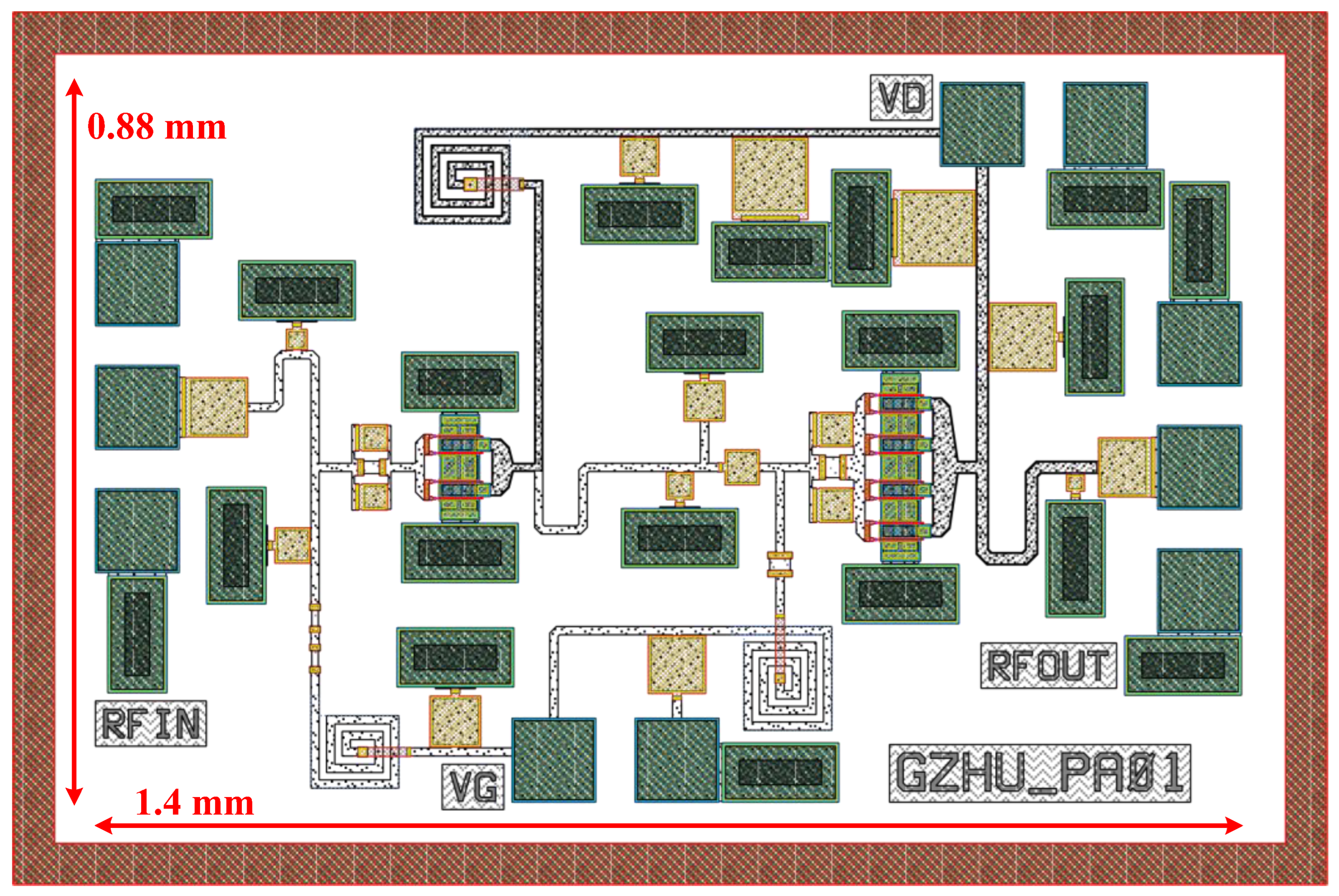
3. Broadband PA Implementation

According to the design specifications, process characteristics, and simulation evaluation, a cascaded two-stage common-source amplifier architecture is adopted, with a device periphery ratio of 1:2 to guarantee a sufficient driving capability. All transistors operate in class AB mode, biased at the recommended gate and drain voltages of −1 V and 12 V, respectively, to achieve a compromise between efficiency and linearity while preserving high-frequency gain. In addition, an appropriate parallel RC network is connected in series at the gate of each transistor, which not only enhances the in-band stability and suppresses parasitic oscillations but also compensates for the gain roll-off to help extend the bandwidth of the PA and facilitates input impedance adjustments for improved matching with the preceding stage, thereby lowering the reflection coefficient. Based on load-pull simulations, Cout of the transistors in the power stage and the driver stage is extracted as 0.27 pF and 0.13 pF, respectively, with the corresponding optimal intrinsic load (Ropt) determined to be 26 Ω and 75 Ω [16]. Using the Bode–Fano criterion, the theoretical bandwidth limit can thus be derived. This section will mainly discuss the design of broadband MNs.

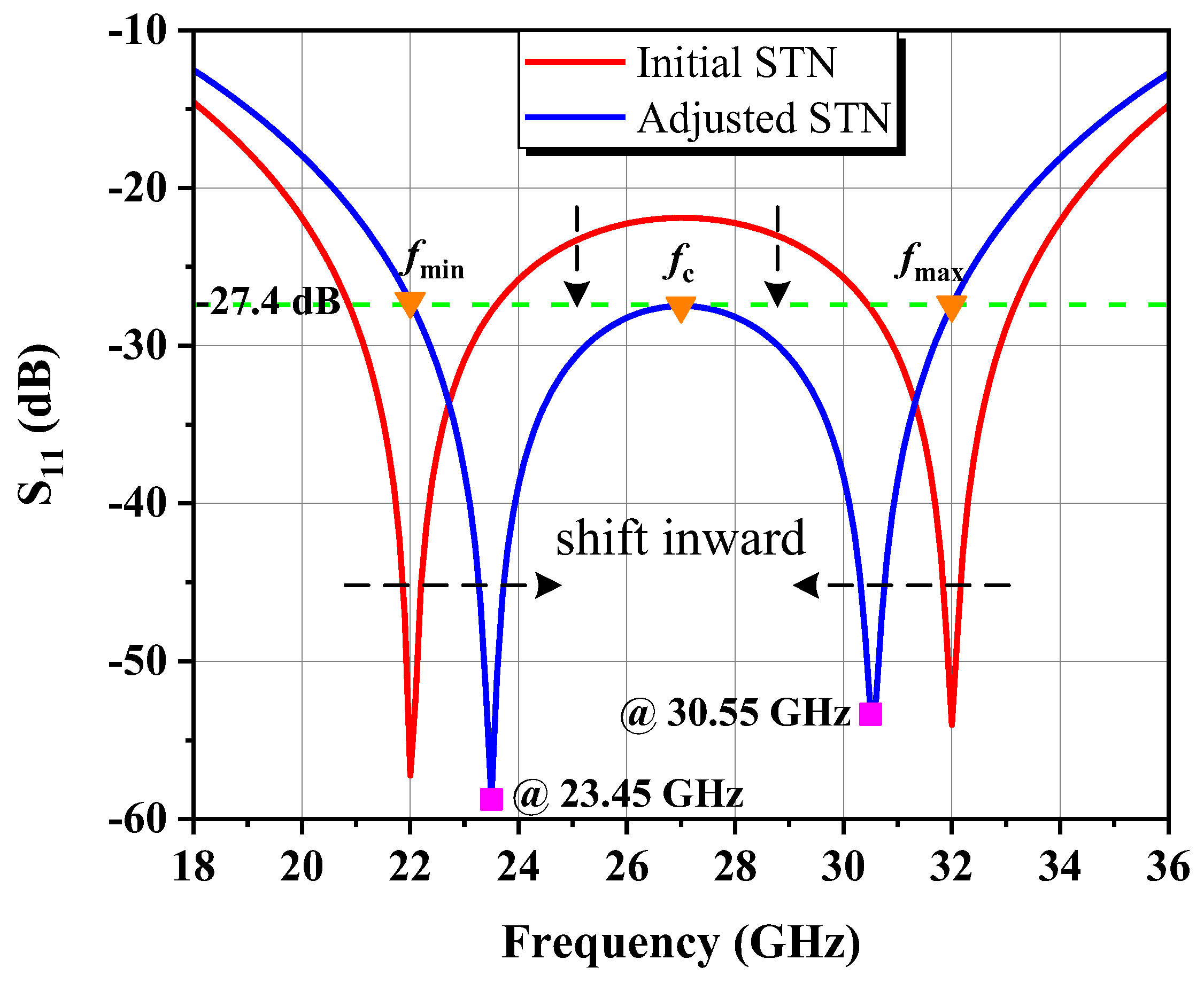
3.1. The Synthesized Transformer Output Matching Network

A large-signal output model of the transistor can be approximated using a parallel RoptCout network, where Cout is the main contributor to the frequency-dependent nature of Zopt(fi) and is the key limitation on the bandwidth. To mitigate this, a synthesized transformer matching technique is applied to absorbing Cout into the OMN [28,29]. This method not only eliminates the need for extra compensation components but also leverages Cout as a beneficial element, resulting in a simpler MN, a lower insertion loss, and improved broadband matching.
The synthesized transformer network (STN) originates from a magnetic coupling resonance model, illustrated in Figure 4a, where both LC resonators resonate at the same angular frequency ω0. The transformer, with an ITR of T and mutual inductance M, can be equivalently represented as the T-type inductor network described in Figure 4b, where M is determined by the coupling coefficient k. By setting the terminal resistances of the STN to Ropt and RL and assigning C2 to Cout, the following relationships are obtained:
T = R L R opt = L 1 L 2 = C out C 1
M = k L 1 L 2
ω 0 = 1 / L 1 C 1 = 1 / L 2 C out
L 1 M > 0 L 2 M > 0
Taking the red dashed plane outlined in Figure 4b as the reference boundary, the admittances seen from both sides of the plane are made conjugate, as expressed in Equation (18), where YL = 1/RL. This condition enables the maximum power transfer. By substituting Equations (14)–(16) into Equation (18) and performing algebraic manipulation, the lower and upper resonance frequencies (fL and fH) of the STN can be derived, as given by Equations (19) and (20), where Qd = 1/(ω0 Ropt Cout).
Y A = 1 R opt = Y A * = Y B = j ω C out + 1 ω 2 L 1 C 1 + j ω L 1 Y L j ω L 2 ω 2 j ω C 1 + Y L L 1 L 2 M 2
f L = ω 0 2 π Q d 2 + Q d 2 k 2 + 2 Q d 2 1 k 2 2 2 4 1 k 2 2 1 k 2
f H = ω 0 2 π Q d 2 + Q d 2 k 2 + 2 + Q d 2 1 k 2 2 2 4 1 k 2 2 1 k 2
Assigning fL and fH to the lower and upper edge frequencies of the BWd (fmin = 22 GHz, fmax = 32 GHz) and using the known design parameters (RL, Ropt, and Cout), together with the relevant derived equations, the remaining component values in the STN can be solved. The results comply with the physical implementation condition described in Equation (17). Subsequently, fL and fH are simultaneously moved toward the center frequency fc (27 GHz) in small steps of 0.05 GHz, with the STN parameters updated in tandem. The iteration proceeds until the S11 of the STN at fmin, fc, and fmax becomes equal. The STN parameters before and after the adjustment of the resonance frequencies are summarized in Table 3. The comparison curves in Figure 5 reveal that the STN provides the optimal S11 response at fL and fH, and a larger separation between the two resonance frequencies results in a more pronounced upward curvature in the central part of the curve, with its peak appearing at fc. Therefore, to minimize the reflected energy, the resonance frequencies are adjusted closer together so that S11 stays below −27 dB throughout the BWd.
To complete the OMN topology, a DC-blocking capacitor C2 with an initial value of 2 pF was added to the adjusted STN, as depicted in Figure 4b, with the inductor M serving as the drain bias line. In the end, optimization of the OMN’s parameters was carried out by applying the aforementioned rapid dual-objective optimization method combined with the PSO algorithm, leading to a notable reduction in the final Etol to 0.3, compared to the Eini of 0.73. Figure 6 shows the trajectory of Zomn(fi), where only at 22 GHz does the transformed impedance fall outside the S-OID, while at mid and high frequencies, Zomn(fi) closely matches the respective Zopt,s(fi). Although the deviation between Zomn(fi) and Zopt,s(fi) is somewhat greater at lower frequencies, Zomn(fi) remains within the P-OID. Such a deliberate matching strategy ensures compliance with large-signal performance requirements over the BWd and a flat frequency response.

3.2. Interstage and Input Matching Network Design

After replacing the OMN and the gate-side parallel RC stabilization network with their respective EM models, a 46 × 8 μm cell was added to perform source-pull simulations for the maximum PAE. The distribution of the resulting optimal source impedance can be characterized as a series RLC circuit, which serves as one end of the interstage matching network (ISMN), while the other end corresponds to the large-signal output equivalent circuit of a 46 × 4 μm cell, which is represented by the parallel RoptCout network. Although the STN can be extended to higher-order configurations to introduce more resonance frequencies for broadband matching, its inherent topological characteristics render it unsuitable for an asymmetric ISMN. To determine the topology and component values of the broadband ISMN, a parametric matching technique based on generalized parallel and series LC units is adopted, wherein the reactance of each series or parallel inductor L or capacitor C is correlated with the phase angle of its reflection coefficient, thereby mapping all possible values of L and C onto a finite and continuous open interval of radians (−π, π) [10]. Such a mapping facilitates the use of CAD tools to swiftly search for the optimal parameter combinations and overcome convergence difficulties, with the optimization objectives set analogously to those in the OMN case. As for the input matching network (IMN), its primary target is to achieve conjugate matching between the transistor’s input impedance and the 50 Ω source to minimize the input reflection. Equally, it should also be capable of assisting in optimizing the gain flatness of the cascaded PA. Since the real part of the small-signal input impedance, as seen from the input side of the stabilized driver-stage transistor, shows little variation, while the imaginary part can be modeled as a series LC circuit, the design of the IMN is accomplished using an analytical approach based on a Chebyshev prototype network and the closed-form solutions supplied in [23].
A schematic of the final PA and its corresponding layout, which passed the design rule check, are shown in Figure 7 and Figure 8, respectively. To minimize the chip area, narrow microstrip lines with widths of 15 μm for the OMN and 10 μm for the other sections were employed. Additionally, the same type of bias supply is provided to both stages through a common square pad, with inductors incorporated to suppress potential signal crosstalk. On-chip bypass capacitors were placed near the power supply pads to mitigate unwanted signal interference and improve the circuit’s stability. To reduce mutual coupling, the spacing between parallel microstrip lines was maintained at a minimum of three times the line width. Furthermore, all bends in the matching microstrip lines were implemented with 45-degree angles to decrease signal reflections. Specifically, double-layer metal was applied to the OMN and the drain bias lines of both stages to enhance the current-carrying capability and reduce the power dissipation and thermal issues caused by ohmic losses. The overall circuit dimensions are 1.4 × 0.88 mm2.

4. Simulation Results

The passive components of the layout, excluding the dicing streets, were simulated using ADS Momentum (a 2.5D planar EM simulator) with a mesh density of 50 cells per wavelength over the DC–100 GHz frequency range. The generated EM model was then integrated with active device library models for circuit–field co-simulation. After rigorous stability verification, the developed PA’s performance was assessed in continuous-wave (CW) mode.

4.1. Small-Signal Characterization

As plotted in Figure 9, S21 varies smoothly from 19.2 to 20.2 dB across 24–31 GHz at room temperature, with a maximum at 25.3 GHz and rapid out-of-band attenuation. Within the same band, S11 and S22 are below −10 dB and −16.7 dB, respectively, each displaying two distinct notches, demonstrating broadband input and output matching characteristics. The fact that the S22 curve exhibits a much deeper notch at 31.4 GHz than that at 25.4 GHz is a direct result of the OMN design strategy, which emphasizes improved high-frequency matching while intentionally introducing some mismatch at lower frequencies to flatten the in-band response. Moreover, S21 declines by no more than 1.2 dB as the temperature rises, with negligible in-band ripple, indicating that the PA maintains a stable small-signal gain across varying temperatures. Although S22 is slightly more susceptible to temperature changes compared to S11, both remain within acceptable tolerance levels.

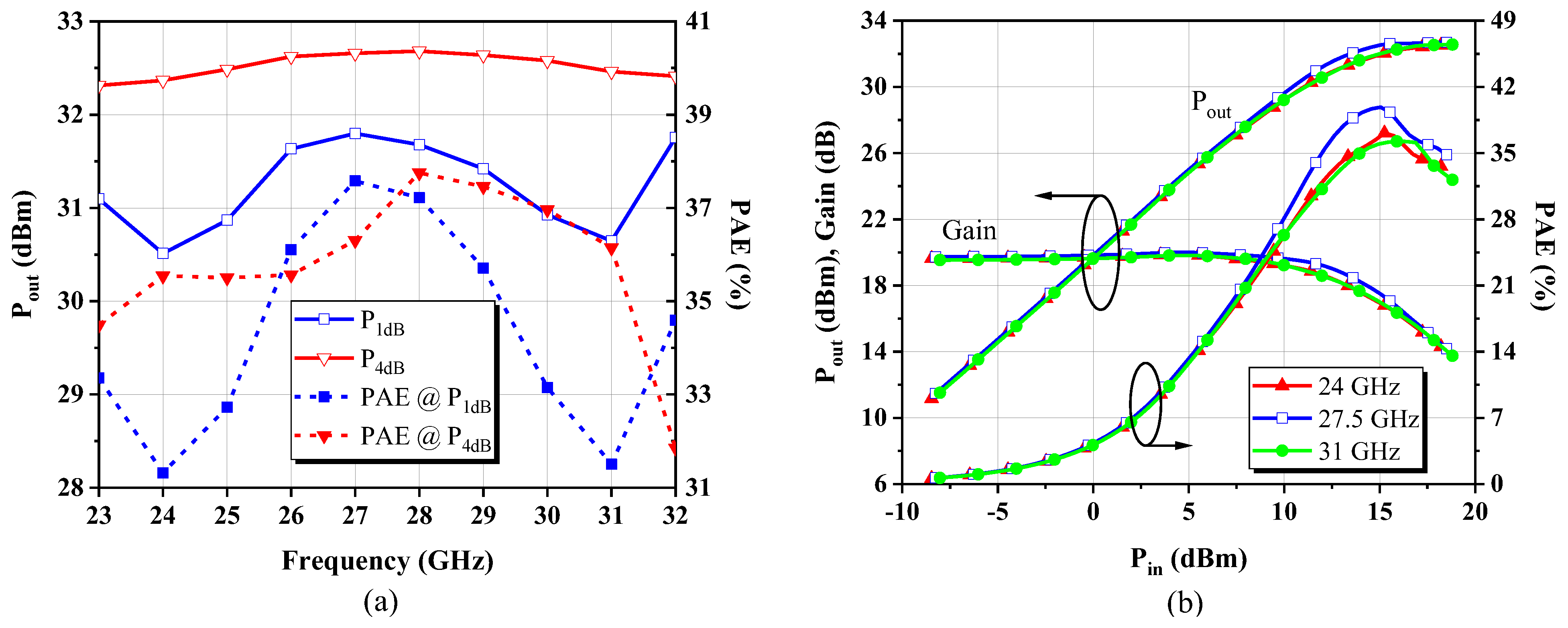
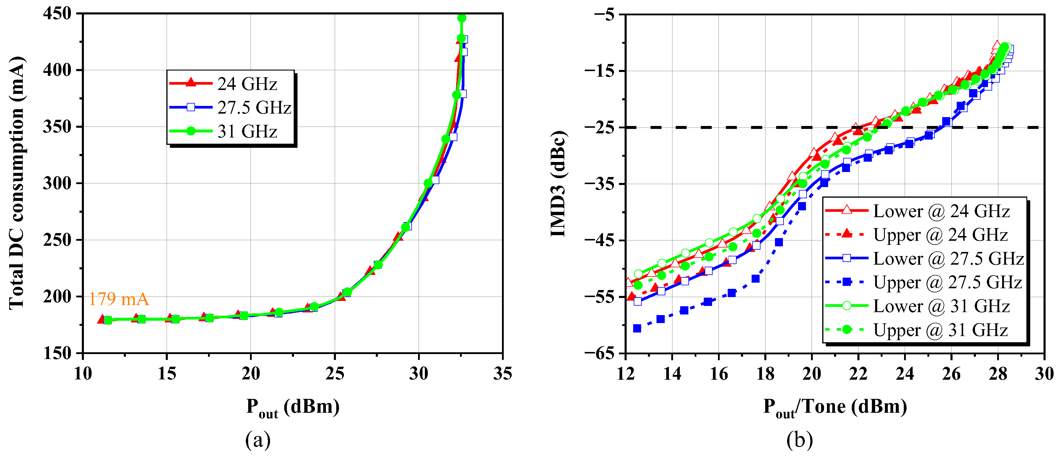
4.2. Large-Signal Characterization

Figure 10a demonstrates that P1dB lies between 30.5 dBm and 31.8 dBm, peaking at 27 GHz, with the corresponding PAE ranging from 31.3% to 37.6% over the 24–31 GHz band. Both of them follow the trend of higher values near the band center and lower values at the band edges. By contrast, P4dB exceeds 32.3 dBm, with a maximum in-band fluctuation of only 0.4 dB, and the associated PAE increases to a range of 35.5–37.8%. Figure 10b presents the power sweep characteristics of the PA, showing that the best performance is achieved at the center frequency, where the peak PAE approaches 40% at an input power (Pin) of 15 dBm, corresponding to P2dB. The responses at low and high frequencies are similar, with the PA reaching a saturation state and the maximum PAE as Pin nears the 4 dB compression point.
Under the preset bias conditions, the quiescent current of the two-stage PA is 179 mA, as described in Figure 11a. The total DC consumption rises markedly as Pout increases beyond 25 dBm, especially in the saturation region, where it peaks at nearly 450 mA. Similar current profiles are obtained at the three representative frequencies, indicating consistent power consumption over the band of interest. Figure 11b displays the IMD3 performance of the PA under two-tone power sweep simulations at 24 GHz, 27.5 GHz, and 31 GHz. The best overall linearity occurs at the center frequency, where the single-tone Pout at an IMD3 of −25 dBc is about 25.6 dBm.
Table 4 summarizes the performance of this work and compares it with recently reported GaAs and GaN PAs operating in similar frequency bands. To enable a comprehensive and relatively robust and fair assessment, a figure of merit (FoM) is introduced, which incorporates all of the parameters listed in the table and considers both high performance and consistency. The FoM is defined as follows:
FoM = FBW % × P out ¯ W × PAE ¯ % Area mm 2 × V DD V × i 1 + Δ x i x i ¯
where FBW is the fractional bandwidth, VDD denotes the supply voltage, and ∆xi and x i ¯ refer to the in-band fluctuation and the mean of each metric (Pout, PAE, and gain), respectively. Note that the gain must be converted from its logarithmic ratio into a linear value before being used in calculations. In contrast to conventional FoM formulas, the cumulative multiplication term added to the denominator serves for evaluating the overall flatness of both large- and small-signal responses, while the use of the average rather than the maximum values for Pout and PAE in the numerator underscores the importance of a balanced broadband performance. The inclusion of the VDD product term in the denominator improves the comparability among varying technologies and supply voltages. As evidenced in Table 4, the proposed mmWave PA demonstrates a superior FoM, achieving the smallest chip size and excellent frequency consistency under similar conditions, reflecting its advanced comprehensive performance.

5. Conclusions

A mmWave PA features multiple critical performance metrics that are often mutually constrained, necessitating the OMN’s design to achieve a balance among them, which is typically accomplished through effective parameter optimization. The conventional strategies usually optimize several large-signal targets directly, which demands resource-intensive HB simulations to assess the response for each OMN parameter set. Additionally, meticulous selection of the target thresholds is essential; otherwise, stringent requirements, excessive objectives, and complicated OMN topologies can easily lead to optimization stagnation or failure, thus hindering design progress. In contrast, the proposed rapid optimization method incorporates only two objectives: all Zomn(fi) must fall inside the OID, and the deviation between Zomn(fi) and Zopt,s(fi) should be minimized. The required large-signal specifications are first mapped to a set of desired impedances, i.e., the OID. Upon satisfying the basic output criteria, adjustments are deliberately made to the matching conditions with the corresponding Zopt,s(fi) at various frequencies, which facilitates the achievement of broadband and uniform output characteristics.
To conclude, the proposed dual-objective optimization strategy utilizes rapid S-parameter simulations to obtain the impedance transformation trajectory, thereby predicting the transistor’s large-signal behavior. Although this method cannot provide precise performance evaluations or the specific deviation from the target, the considerable savings in the simulation time greatly benefit optimization tasks involving numerous iterations. Equally, acquiring detailed trial-and-error performance data is not necessary for the overall optimization effectiveness. Thanks to its high optimization efficiency and fully automated iterative process, the proposed method allows for a convenient assessment of the matching capabilities across various OMN topologies, significantly boosting both the design efficiency and success rate. For different terminal impedance model circuits, OMN, ISMN, and IMN, respectively, employ the synthesized transformer matching technique, the parametric matching technique, and a bandpass-filter-based matching structure to accomplish broadband impedance transformation with limited component usage.
The implemented two-stage PA occupies a compact footprint of 1.23 mm2 and delivers a small-signal gain averaging 19.7 dB with less than 1 dB fluctuations over the 24–31 GHz band, exhibiting excellent broadband matching characteristics. Moreover, it demonstrates good temperature stability and features a flat P4dB of at least 32.3 dBm, along with a high associated PAE, reaching a peak PAE close to 40%. The adoption of a silicon substrate process endows the GaN PA with significant cost effectiveness, making it well suited to mass production and compatible with mainstream CMOS fabrication technologies, thereby facilitating multifunctional and heterogeneous integration. As a result, the proposed MMIC PA not only meets the stringent SWaP-C requirements of millimeter-wave applications such as 5G-A wireless communications and SATCOM but is also ideal for highly integrated T/R-module front ends.

Author Contributions

Conceptualization: L.P.; methodology: L.P.; software: L.P. and Z.Y.; validation: L.P., Z.Y., Y.Z., C.Z. and Y.F.; formal analysis: L.P. and Z.Y.; investigation: L.P., Z.Y., Y.Z., C.Z. and Y.F.; resources: L.P.; data curation: L.P. and Z.Y.; writing—original draft preparation: L.P. and Z.Y.; writing—review and editing: L.P.; visualization: L.P.; supervision: J.Q. and Y.L.; project administration: J.Q. and Y.L.; funding acquisition: J.Q. and Y.L. All authors have read and agreed to the published version of the manuscript.

Funding

This research was funded by the Provincial Key College Student Innovation Training Program of Guangzhou University, grant number 202511078067, the National College Student Innovation Training Program of Guangzhou University, grant number 202411078009, and the Guangzhou Science and Technology Plan Project, grant number 2024A03J0326.

Data Availability Statement

The original contributions presented in this study are included in the article. Further inquiries can be directed to the corresponding author(s).

Conflicts of Interest

The authors declare no conflicts of interest.

Abbreviations

The following abbreviations are used in manuscript:
3GPPThird-generation partnership project
5GFifth-generation mobile communication network
5G-A5G-Advanced
ADSAdvanced design system
CADComputer-aided design
CMOSComplementary metal oxide semiconductor
CWContinuous-wave
EMElectromagnetic
FBWFractional bandwidth
FoMFigure of merit
FRFrequency range
GaAsGallium arsenide
GaNGallium nitride
GaN-on-SiGallium nitride-on-silicon
HBHarmonic balance
HEMTHigh-electron-mobility transistor
IMD3Third-order intermodulation distortion
IMNInput matching network
ISMNInterstage matching network
ITRImpedance transformation ratio
MMICMonolithic microwave integrated circuit
mmWaveMillimeter-wave
MNMatching network
OIDOptimal impedance domain
OMNOutput matching network
OPGOperating power gain
PAPower amplifier
PAEPower-added efficiency
P-OIDPreferred optimal impedance domain
PSOParticle swarm optimization
SATCOMSatellite communication
SOISilicon-on-insulator
S-OIDStrict optimal impedance domain
SRFTSimplified real-frequency technique
STNSynthesized transformer network
SWaP-CSize, weight, power, and cost

References

  1. Azari, M.M.; Solanki, S.; Chatzinotas, S.; Kodheli, O.; Sallouha, H.; Colpaert, A.; Mendoza Montoya, J.F.; Pollin, S.; Haqiqatnejad, A.; Mostaani, A.; et al. Evolution of Non-Terrestrial Networks from 5G to 6G: A Survey. IEEE Commun. Surv. Tutorials 2022, 24, 2633–2672. [Google Scholar] [CrossRef]
  2. Xiao, Y.; Ye, Z.; Wu, M.; Li, H.; Xiao, M.; Alouini, M.-S.; Al-Hourani, A.; Cioni, S. Space-Air-Ground Integrated Wireless Networks for 6G: Basics, Key Technologies, and Future Trends. IEEE J. Sel. Areas Commun. 2024, 42, 3327–3354. [Google Scholar] [CrossRef]
  3. He, S.; Zhang, Y.; Wang, J.; Zhang, J.; Ren, J.; Zhang, Y.; Zhuang, W.; Shen, X. A Survey of Millimeter-Wave Communication: Physical-Layer Technology Specifications and Enabling Transmission Technologies. Proc. IEEE 2021, 109, 1666–1705. [Google Scholar] [CrossRef]
  4. Longhi, P.E.; Pace, L.; Costanzo, F.; Ciccognani, W.; Colangeli, S.; Giofrè, R.; Leblanc, R.; Suriani, A.; Vitobello, F.; Limiti, E. 32–36-GHz Single-Chip Front-End MMIC Featuring 35-dBm Output Power and 3.2-dB Noise Figure with 60- and 100-Nm GaN/Si HEMTs. IEEE Trans. Microw. Theory Tech. 2024, 72, 160–172. [Google Scholar] [CrossRef]
  5. Sonnenberg, T.; Romano, A.; Miller, N.C.; Popović, Z. A W-Band GaN MMIC Single-Chip T/R Front End. IEEE Trans. Microw. Theory Tech. 2024, 72, 5830–5837. [Google Scholar] [CrossRef]
  6. Nikandish, R. GaN Integrated Circuit Power Amplifiers: Developments and Prospects. IEEE J. Microw. 2023, 3, 441–452. [Google Scholar] [CrossRef]
  7. Jeong, H.; Lee, H.D.; Park, B.; Jang, S.; Kong, S.; Park, C. Three-Stacked CMOS Power Amplifier to Increase Output Power with Stability Enhancement for Mm-Wave Beamforming Systems. IEEE Trans. Microw. Theory Tech. 2023, 71, 2450–2464. [Google Scholar] [CrossRef]
  8. Kim, K.; Choi, I.; Lee, K.; Choi, S.-U.; Kim, J.; Choi, C.-G.; Song, H.-J. Analysis and Design of Multi-Stacked FET Power Amplifier with Phase-Compensation Inductors in Millimeter-Wave Band. IEEE Trans. Microw. Theory Tech. 2023, 71, 1877–1889. [Google Scholar] [CrossRef]
  9. Fu, Z.-H.; Li, M.-X.; Ma, T.-G.; Wu, C.-S.; Lin, K.-Y. Millimeter-Wave GaAs Ultra-Wideband Medium Power Amplifier and Broadband High-Power Power Amplifier for 5G/6G Applications. IEEE J. Emerg. Sel. Top. Circuits Syst. 2024, 14, 111–121. [Google Scholar] [CrossRef]
  10. Meghdadi, M.; Medi, A. Design of 6–18-GHz High-Power Amplifier in GaAs pHEMT Technology. IEEE Trans. Microw. Theory Tech. 2017, 65, 2353–2360. [Google Scholar] [CrossRef]
  11. Shi, J.; Fang, X.; Yu, H.; Sui, J.; Cheng, K.-K.M. Novel Wideband Millimeter-Wave GaN Power Amplifier Design Using Transistors with Large Drain Capacitance and High Optimum Load Impedance. IEEE Trans. Circuits Syst. II 2023, 70, 4309–4313. [Google Scholar] [CrossRef]
  12. Zhao, Z.; Zhu, X.; Xia, J.; Liu, R.; Dong, Q.; Chen, P.; Zhang, L.; Jiang, X.; Yu, C.; Hong, W. A 23–29.5 GHz Three-stage Mm-wave GaN Power Amplifier Using Arbitrary Two-port Complex-impedance Matching Method. Circuit Theory Appl. 2023, 51, 5103–5115. [Google Scholar] [CrossRef]
  13. Cai, Q.; Zhu, H.; Zeng, D.; Xue, Q.; Che, W. A Three-Stage Wideband GaN PA for 5G Mm-Wave Applications. IEEE Trans. Circuits Syst. II 2022, 69, 4724–4728. [Google Scholar] [CrossRef]
  14. Peng, L.; Yan, J.; Zhang, Z.; Zhang, G. An Efficient 24–30 GHz GaN-on-Si Driver Amplifier Using Synthesized Matching Networks. Micromachines 2023, 14, 175. [Google Scholar] [CrossRef]
  15. Wang, K.; Xu, J.-X.; Zhang, X.Y. A 24–31 GHz GaN-on-Si Power Amplifier MMIC. In Proceedings of the 2021 IEEE International Workshop on Electromagnetics: Applications and Student Innovation Competition (iWEM), Guangzhou, China, 28–30 November 2021; pp. 1–3. [Google Scholar]
  16. Peng, L.; Chen, J.; Zhang, Z.; Zhang, G. Design of an Efficient 24–30 GHz GaN MMIC Power Amplifier Using Filter-Based Matching Networks. Electronics 2022, 11, 1934. [Google Scholar] [CrossRef]
  17. Yan, X.; Zhang, J.; Lv, G.; Chen, W.; Guo, Y. Gain and Power Enhancement with Coupled Technique for a Distributed Power Amplifier in 0.25- Μm GaN HEMT Technology. IEEE Trans. VLSI Syst. 2024, 32, 1523–1534. [Google Scholar] [CrossRef]
  18. Chen, K.; Peroulis, D. Design of Highly Efficient Broadband Class-E Power Amplifier Using Synthesized Low-Pass Matching Networks. IEEE Trans. Microw. Theory Tech. 2011, 59, 3162–3173. [Google Scholar] [CrossRef]
  19. Yang, M.; Xia, J.; Guo, Y.; Zhu, A. Highly Efficient Broadband Continuous Inverse Class-F Power Amplifier Design Using Modified Elliptic Low-Pass Filtering Matching Network. IEEE Trans. Microw. Theory Tech. 2016, 64, 1515–1525. [Google Scholar] [CrossRef]
  20. Zhang, X.; Li, S.; Huang, D.; Chi, T. A Millimeter-Wave Three-Way Doherty Power Amplifier for 5G NR OFDM. IEEE J. Solid-State Circuits 2023, 58, 1256–1270. [Google Scholar] [CrossRef]
  21. Yarman, B.S.; Carlin, H.J. A Simplified “Real Frequency” Technique Applied to Broad-Band Multistage Microwave Amplifiers. IEEE Trans. Microw. Theory Tech. 1982, 30, 2216–2222. [Google Scholar] [CrossRef]
  22. Matthaei, G.L. Tables of Chebyshev Impedance–Transforming Networks of Low-Pass Filter Form. Proc. IEEE 1964, 52, 939–963. [Google Scholar] [CrossRef]
  23. Dawson, D.E. Closed-Form Solutions for the Design of Optimum Matching Networks. IEEE Trans. Microw. Theory Tech. 2009, 57, 121–129. [Google Scholar] [CrossRef]
  24. Meng, X.; Yu, C.; Liu, Y.; Wu, Y. Design Approach for Implementation of Class-J Broadband Power Amplifiers Using Synthesized Band-Pass and Low-Pass Matching Topology. IEEE Trans. Microw. Theory Tech. 2017, 65, 4984–4996. [Google Scholar] [CrossRef]
  25. Saad, P.; Fager, C.; Cao, H.; Zirath, H.; Andersson, K. Design of a Highly Efficient 2–4-GHz Octave Bandwidth GaN-HEMT Power Amplifier. IEEE Trans. Microw. Theory Tech. 2010, 58, 1677–1685. [Google Scholar] [CrossRef]
  26. Kuwata, E.; Alimohammadi, Y.; Liu, X.; Bell, J.; Tasker, P.; Shinjo, S.; Benedikt, J. Effects of Load Impedances at Third Order Intermodulation Tones. In Proceedings of the 2020 15th European Microwave Integrated Circuits Conference (EuMIC), Utrecht, The Netherlands, 10–15 January 2020; pp. 201–204. [Google Scholar]
  27. Ghanipour, P.; Stapleton, S.; Kim, J.-H. Load–Pull Characterization Using Different Digitally Modulated Stimuli. IEEE Microw. Wireless Compon. Lett. 2007, 17, 400–402. [Google Scholar] [CrossRef]
  28. Huang, P.-C.; Tsai, Z.-M.; Lin, K.-Y.; Wang, H. A 17–35 GHz Broadband, High Efficiency PHEMT Power Amplifier Using Synthesized Transformer Matching Technique. IEEE Trans. Microw. Theory Tech. 2012, 60, 112–119. [Google Scholar] [CrossRef]
  29. Chen, Y.; Wu, Y.; Luo, L.; Wang, Q.; Zhang, Y.; Yan, B.; Xu, R.; Xu, Y. Design of 18–40 GHz GaN Reactive Matching Power Amplifiers Using One-order and Two-order Synthesised Transformer Networks. IET Microw. Antennas Propag. 2022, 16, 78–90. [Google Scholar] [CrossRef]
Figure 1. (a) Load-pull simulation results at the 1 dB compression point and the determination of OID; (b) OPG contours of 6.85 dB within the BWd and the determination of P-OID.
Electronics 14 02996 g001
Figure 2. IMD3 load-pull contours and the determination of S-OID.
Electronics 14 02996 g002
Figure 3. A flowchart of the parameter optimization method for the OMN.
Electronics 14 02996 g003
Figure 4. STN: (a) magnetic coupling resonance model; (b) equivalent T-network.
Electronics 14 02996 g004
Figure 5. Reflection coefficients of the initial and adjusted STN.
Electronics 14 02996 g005
Figure 6. The transformation features of the optimized OMN from 22 to 32 GHz.
Electronics 14 02996 g006
Figure 7. A schematic diagram of the two-stage PA.
Electronics 14 02996 g007
Figure 8. The complete layout of the GaN MMIC PA.
Electronics 14 02996 g008
Figure 9. The simulated (a) S21, (b) S11, and (c) S22 at different temperatures.
Electronics 14 02996 g009
Figure 10. The simulated (a) Pout and PAE at 1 dB and 4 dB compression points; (b) Pout, PAE, and gain behaviors with respect to Pin.
Electronics 14 02996 g010
Figure 11. The simulated (a) total DC consumption versus Pout; (b) two-tone power sweep with a 100 MHz frequency spacing.
Electronics 14 02996 g011
Table 1. The optimal load impedances obtained via load-pull simulations and calculations.
fi (GHz)U1(fi) (Ω)U2(fi) (Ω)Zopt,s(fi) (Ω)
2215.6 + j12.315.4 + j16.815.5 + j15.3
2414.1 + j13.113.9 + j16.414.0 + j15.3
2614.3 + j11.212.9 + j15.513.4 + j14.1
2812.8 + j10.411.5 + j14.211.9 + j12.9
3012.7 + j9.810.9 + j12.511.5 + j11.6
3212.2 + j8.69.3 + j11.210.3 + j10.3
Table 2. Weight allocation for matching error based on PAE differences.
fi (GHz)Zopt,s(fi) (Ω)PAE (%)wi
2215.5 + j15.354.020.115
2414.0 + j15.352.580.133
2613.4 + j14.151.340.151
2811.9 + j12.950.030.172
3011.5 + j11.648.730.196
3210.3 + j10.346.970.234
Table 3. The parameters of the STN.
RoptCoutL2-MML1-MC1RL
Initial26 Ω0.27 pF0.9 pH190.47 pH177.56 pH0.14 pF50 Ω
Adjusted26 Ω0.27 pF6.19 pH176.35 pH174.69 pH0.14 pF50 Ω
Table 4. Performance summary and comparisons with contemporary works.
Ref.[9][11][12][13][14][15]This Work
Process0.15 μm GaAs0.15 μm GaN/SiC0.15 μm GaN/SiC0.1 μm GaN/Si0.1 μm GaN/Si0.1 μm GaN/Si0.1 μm GaN/Si
BW. (GHz)24–3224.5–2923–29.524–2924–3024–3124–31
FBW (%)28.616.824.818.922.225.525.5
Supply (V)5282012121212
Gain (dB)16.5 ± 0.511.5 ± 2.232.5 ± 2.520 ± 1.319.3 ± 125.5 ± 1.519.7 ± 0.5
Pout (dBm)29 ± 0.629.8 ± 0.434.1 ± 0.830.7 ± 0.730.6 ± 0.534.3 ± 0.332.5 ± 0.2
PAE (%)27–33 b28.3–42.8 c24.7–39.1 c27.6–38.9 b30.9–39.8 a35.8–37.4 b35.5–37.8 a
Size (mm2)2.4 × 1.12.1 × 1.33.4 × 1.92.2 × 1.31.65 × 0.783.25 × 11.4 × 0.88
FoM41.84.410.815.845.761.3104.3
a PAE @ specific gain compression point. b PAE @ specific input drive. c peak PAE.
Disclaimer/Publisher’s Note: The statements, opinions and data contained in all publications are solely those of the individual author(s) and contributor(s) and not of MDPI and/or the editor(s). MDPI and/or the editor(s) disclaim responsibility for any injury to people or property resulting from any ideas, methods, instructions or products referred to in the content.

