1. Introduction
Today’s power supplies for industrial use face several requirements, especially concerning efficiency and compliance with limit values from EMC standards. When used with rotating machines, such as servo drives, the capability of bidirectional energy flow plays an equally important role, avoiding the waste of braking energy with a bleeder resistor. VSIs are the means of choice to meet these requests, which also results in further advantages, e.g., controlled DC-link voltage and power factor correction. The three-level topologies provide lower harmonic content compared to two level inverters [
1], which is a great advantage as they save on expensive, heavy and space-consuming filter components. This comes at the cost of an increased use of power semiconductors, which, in contrast, are becoming ever cheaper, smaller and more powerful. The T-type topology has emerged as best suited for grid applications concerning the number of switches and efficiency [
2]. This is mainly due to the fact that, unlike motor drive applications, higher modulation degrees are always needed, involving only one switch for the outer voltages as opposed to other three-level topologies. To achieve this, the voltage rating of the outer switches needs to block the full DC-link voltage, which in turn allows current GaN devices with up to 650 V only for the inner switches.
For the evaluation of eligible devices, the DPT is one major method to characterise the switching performance of a power transistor. Nevertheless, the switching loss measurement with DPT has limited significance when used with fast-switching GaN devices, because measurement errors can easily reach >100% [
3]. Besides the temporal mismatch of the current and voltage measurement signals, the correct and non-invasive measurement of the drain current is challenging or, in high-density designs or power modules, not feasible [
4]. In situ current sense methods can be used to mitigate these issues [
5]. Another characterisation method to overcome this sensitivity is the use of the OM [
6], which uses a power measurement at the slow-varying DC input of a H-bridge configuration. For the calculation of the losses within a switching cell, all other occurring losses (e.g., inductor losses) need to be known and subtracted from the measured values. At first glance, this gives only the total losses of the inverter. But, by varying the operating conditions, the losses measured on the DC side can be divided into the different loss mechanisms for turn-on, turn-off and conduction.
This article presents a complete workflow for designing, testing and evaluating the performance of GaN transistors in a T-type configuration. For this purpose, the design and verification of a corresponding evaluation board in the form of a PCB are discussed in detail, focusing on the minimisation of parasitic elements, which is essential for the successful and optimal operation of GaN transistors. Various simulation and calculation methods, as well as verification through measurement, are presented. For the evaluation board, it was necessary to operate the GaN transistors in parallel to increase the current capability, which is why the special aspects of the parallel operation of GaN transistors are also covered in this article. Another aspect of this work is the implementation of the modulation and control algorithms for the OM test in an FPGA, which is also presented. Finally, the test bench for the practical measurements on fast switching GaN in DPT and OM, with corresponding results, is presented and discussed.
2. Phase Leg Design
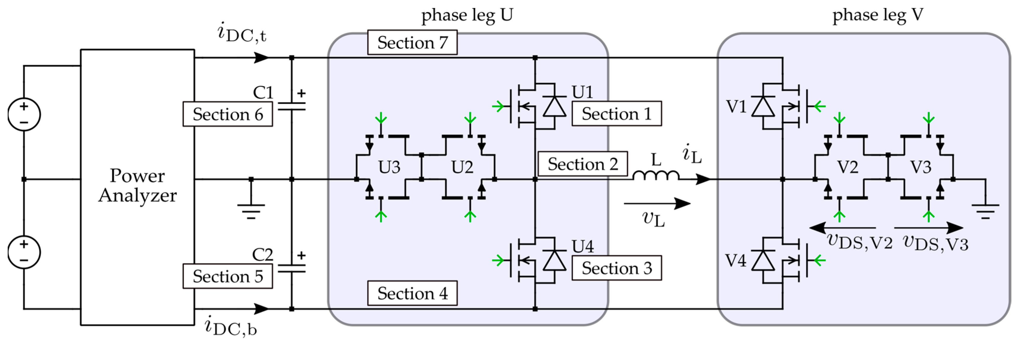
The evaluation board, whose schematic is shown in
Figure 1, serves as a pre-investigation for a demonstrator, which comprises an entire three-phase VSI. The results obtained for one single phase can be projected onto the other phases. For the GaN devices, 20 mΩ HEMTs in a top-side cooled LFPAK package from ST Microelectronics (Plan-les-Ouates, Switzerland) were used. One requirement is a maximum load current of 90 A, which is only feasible with a parallel connection of GaN transistors.
In parallel GaN HEMT configurations, natural current balancing tends to occur during the on-state due to the positive temperature coefficient of the on-state resistance (
). Devices with initially lower
heat up more quickly, increasing their resistance and promoting uniform current distribution [
7].
The threshold voltage (Vth) significantly influences the dynamic current sharing among devices. Devices with lower Vth switch earlier, resulting in higher turn-on losses and lower turn-off losses. However, this behaviour is independent of thermal imbalances among the devices [
7,
8].
The high dV/dt and dI/dt characteristics of GaN HEMTs render PCB parasitics—particularly in the power and gate driver loops—crucial to device performance and reliability. Minimising these parasitics helps reduce voltage overshoots, EMI, and switching losses [
8,
9]. In addition to addressing the well-documented parasitics from single-device switching, specific routing considerations must be prioritised to enhance the dynamic performance and balance of paralleled GaN HEMTs. Parallel operation introduces additional complexity since mismatched parasitics can lead to uneven switching behaviour and degraded performance.
Special attention must be given to PCB layout. An unbalanced gate driver loop can cause variations in gate voltage slew rates, leading to asynchronous switching. The quasi-common source inductance can help balance dynamic current by reducing
in faster devices but may also introduce overshoot or ringing due to feedback [
8,
10].
In summary, for the parallelisation of GaN devices, it is recommended to minimise all stray inductances in the power and gate driver loops. Additionally, achieving symmetry in the inductances of both the power loop and gate driver loop is crucial for optimal performance.
Therefore, significant effort was dedicated to the design of the switching cell to fully exploit the high-speed switching capabilities of GaN devices and to ensure symmetry among parallel-connected devices. A multi-layer PCB with microvia interconnections was implemented to minimise loop area, which is constrained by the inter-layer spacing.
Since the minimization of such stray elements are very important two different estimation methods will be presented and compared. Two simulation cases, and one analytical calculation and finally they will be compared with measurements.
2.1. Analytical Calculation of Power Loop Inductance
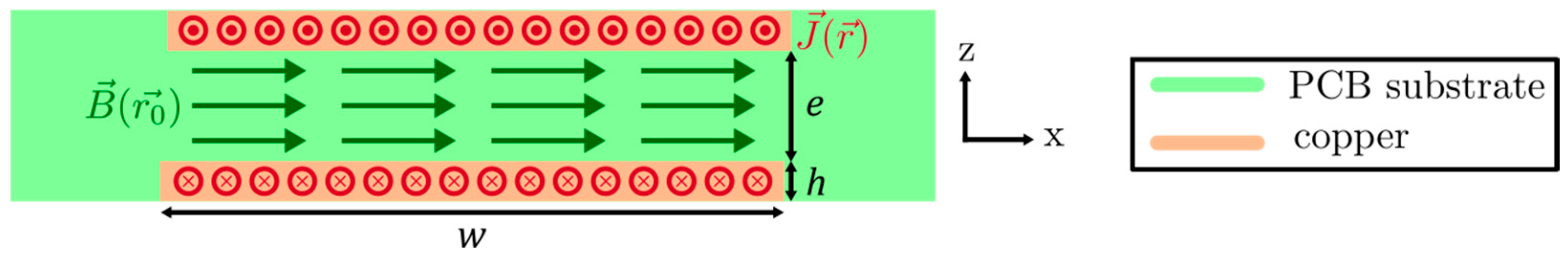
Based on the Biot–Savart law, Equation (1) [
11] provides an excellent inductance calculation for two copper traces on top of each other. The authors evaluate the field distribution
in any given point in space
under the circumstance of infinite long traces, as is customary in conductor theory. A current density
, which is considered constant, describes the magnetic field’s source inside a volume
. The given assumptions form the basis for a quasi-stationary field calculation. Through proper integration of
over an area for finite long traces (
), the authors finally derive Equation (2) [
11] to calculate the parasitic inductance on a PCB solely from geometric dimensions. In the equation, the parameters are determined by the length
in y-direction, the width
and the height
of the traces as well as the distance
between the upper and lower trace, with
representing the magnetic field constant. The calculation method is quite charming, since a physical law gives the starting point.
Figure 2 depicts the qualitative distribution of
and
. The current density is constant over the copper cross-section, where the upper and lower trace guide currents in opposite directions. Since
, the magnetic field between the conductor traces is approximately homogeneous with only an x-component. The field outside this volume is negligibly small in comparison. As a PCB does not consist of only two traces with the same width and length, it is useful to subdivide a given layout into multiple sections, where each partial inductance is calculable with Equation (2).
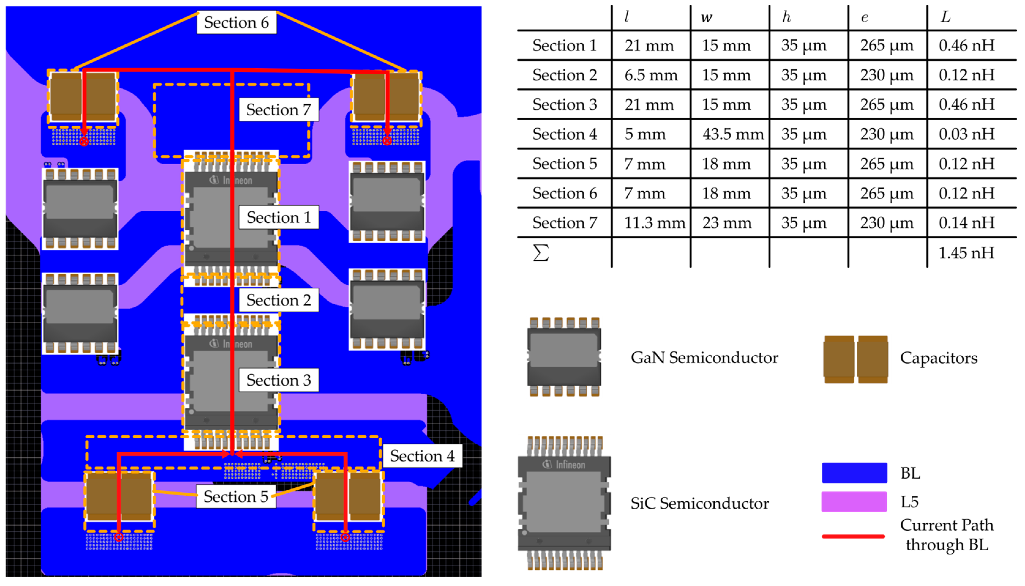
For visualisation,
Figure 3 shows a subdivision of the designed layout and the respective results for each section, as well as the summed loop inductance of
. Single components (see
Figure 1) like MOSFET U1 form one section; for example, just like the nearly rectangular-shaped trace parts on the BL. In this case, a power loop through MOSFETS U1, U4 and capacitors C1, C2 is considered (2-level outer loop). The resulting current path closes via BL and the layer above (L5). Copper plates replace the components in simulation and calculation, which makes an important difference to the real system, because current densities are not comparable. Nevertheless, the suggested procedure should represent the principal behaviour and provide a good estimation. For a more accurate result, the components’ inductances must be determined.
2.2. Simulation of Power Loop Inductance
The simulation process begins by importing the PCB layout into the 3D interface of CST Studio Suite (R2024.05, Dassault Systèmes, Vélizy-Villacoublay, France). To reduce mesh complexity and simulation time, the copper layers are modelled with zero thickness, while the dielectric material properties remain unchanged. This simplification is justified for stray inductance analysis at frequencies corresponding to GaN switching transitions (~10–50 MHz), where the real part of the impedance is negligible. Although zero-thickness modelling may affect low-frequency results, it has minimal impact at high frequencies due to the dominance of skin and proximity effects. At these frequencies, currents flowing in opposite directions tend to concentrate near the surfaces of conductors, particularly on the facing sides of parallel conductors. Thus, the switching current is effectively confined to a thin layer of the conductor.
Each switching device is then replaced by a port, and the S-parameter matrix of the power stage is computed. This matrix is post-processed to derive the admittance (Y) and impedance (Z) matrices, which are used to evaluate the stray inductance of the power loops [
12]. The stray inductances of the top, bottom, and outer loops in this evaluation board are 2.27 nH, 1.97 nH, and 2.77 nH at 30 MHz, respectively.
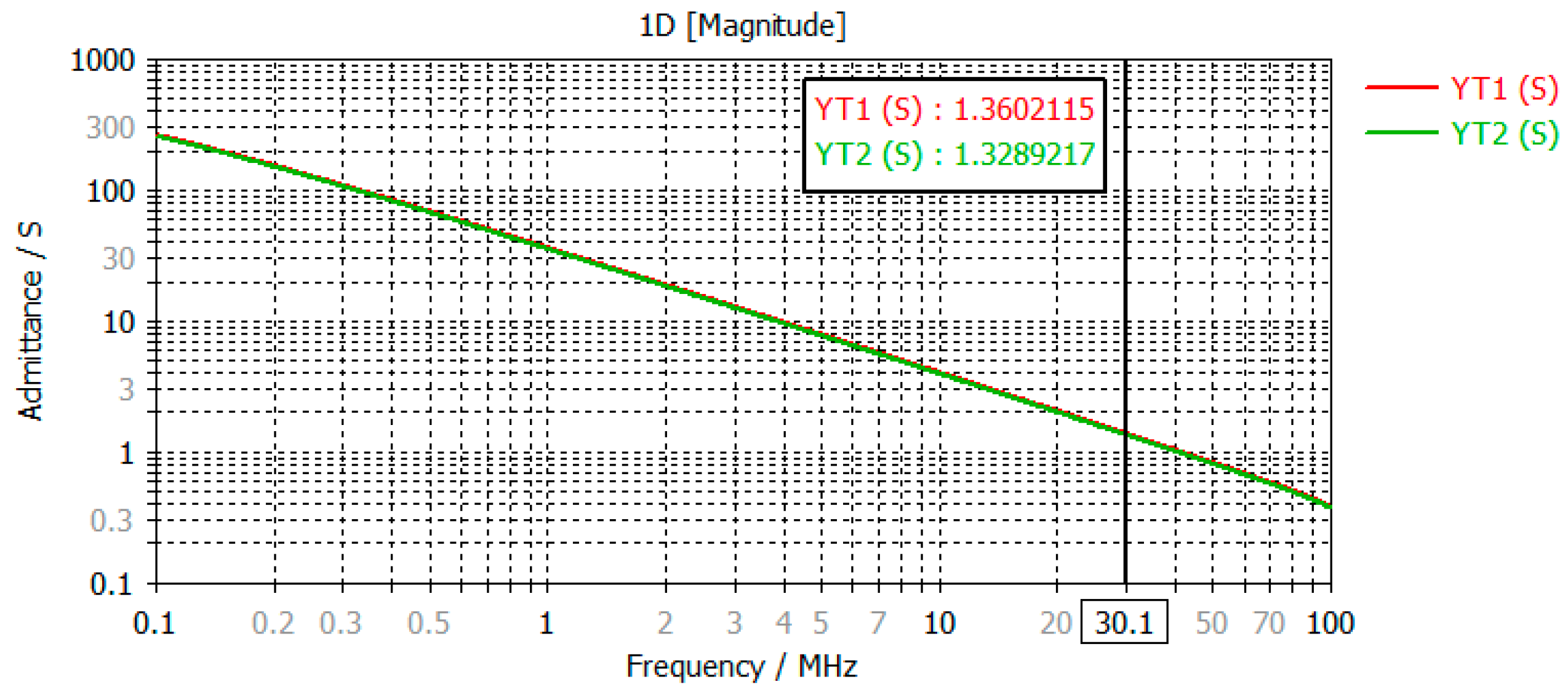
The Y and Z matrices also enable evaluation of symmetry in the layout by comparing the admittance seen by each device in a parallel configuration. For instance,
Figure 4 shows the admittance seen by the two devices forming switch U3. The results indicate a high degree of symmetry, with only minor differences. These discrepancies are primarily due to asymmetries in the device packaging—specifically, the source pins layout influenced by the gate and Kelvin source connection—which slightly alters the surrounding copper plane geometry (see
Figure 3).
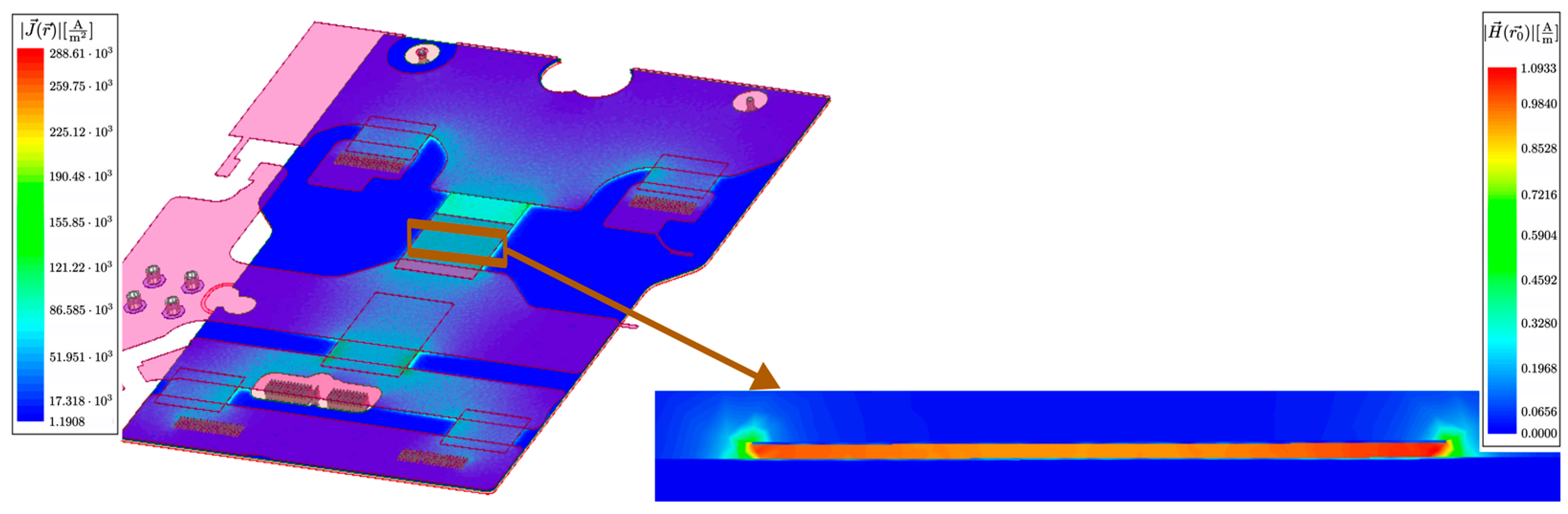
To simulate the stray inductance of the outer loop using Ansys HFSS (Ansys Electronics Desktop 2021 R2.2, Canonsburg, PA, USA), the loop is excited via a small port placed at U1. The resulting current flows through the copper planes and traces located on BL and layer L5. Although the traces on these layers differ in width—unlike the idealised geometry shown in
Figure 5—the simulation results confirm that the current is confined to a narrow region where the copper traces overlap. This behaviour is attributed to the proximity effect, which causes current to concentrate in areas of lowest impedance.
At low frequencies, copper cross-section and length define the structure’s resistance and a larger cross-section results in lower resistance. Hence, the current flows through the whole material, not only in copper overlaying regions of L5 and BL. In this case, most of the electrical energy is converted to heat. As frequency increases, the complex resistance becomes more significant. A state of low energy, small impedance and inductance is reachable with a minimum of magnetic flux. A current, flowing through overlaying copper regions, reaches this state, because magnetic field components occur in between both traces and erase each other outside the gap.
Figure 5 represents the described behaviour by showing the field distribution of
and
from simulation with Ansys HFSS.
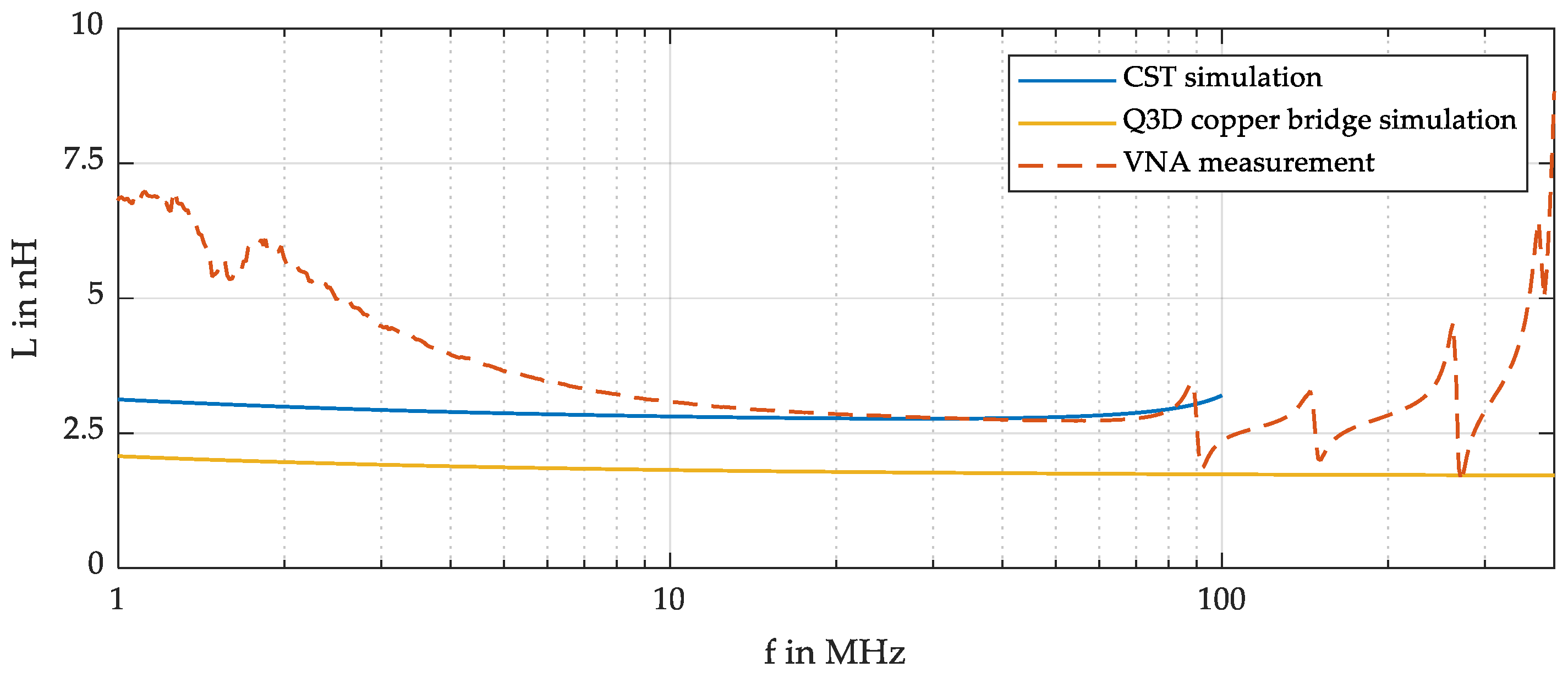
The analytical calculation of the outer loop inductance yields a total value of 1.45 nH, obtained by summing the contributions of individual segments. Ansys HFSS simulation results show a slightly higher inductance of 1.62 nH at 30 MHz, demonstrating good agreement with the analytical approach. This confirms that the analytical method provides a fast and reasonably accurate means of estimating inductance in complex PCB structures without requiring detailed 3D modelling.
In contrast, CST simulation results indicate a higher inductance of 2.6 nH. This discrepancy can be attributed to differences in how the switching devices are modelled. In both the analytical method and the Ansys simulation, the devices are represented by copper planes at the PCB layer level, with widths matching the component footprints. However, in the CST simulation, the devices are modelled using ports positioned at the average height of the actual components. This more realistic representation reduces the mutual inductance between the devices and the PCB, leading to an increase in the overall loop inductance.
2.3. Measurement of Loop Inductance
Finally, a measurement of the bare PCB serves as a confirmation of the calculations, which resulted in values between
for the loop inductance across the methods. Therefore, a VNA, Type E5061B (Keysight Technologies, Santa Rosa, CA, USA) was connected through a calibrated MMCX connector with an inlet on the PCB on which the affected components are replaced by copper foils [
9].
Figure 6 depicts a comparison of the applied methods over the frequency range for the outer loop of the T-type topology.
The CST simulation results show good agreement with the measured data within the frequency range corresponding to the switching transitions of the devices. In the experimental measurements, a frequency-dependent decrease in inductance is observed at lower frequencies, which is attributed to skin and proximity effects—phenomena that were not accounted for in the simulation models. While Ansys Q3D (Ansys Electronics Desktop 2024 R2, Canonsburg, PA, USA) simulation still provides a representative estimate of the stray inductance, the observed discrepancies highlight the impact of geometric simplifications in the simulation setup. These differences emphasise the importance of accurately modelling physical details when predicting parasitic effects in high-frequency power electronics.
Table 1 presents a comparison between simulated loop inductances (using CST) and measured values for the three loops of the T-type converter. The results show good agreement, with a maximum deviation of 16% observed for the bottom loop.
The table also includes loop inductance values from two other studies [
8,
9], which analysed converters using GaN devices in parallel. Compared to these topologies, the evaluated T-type converter exhibits lower stray inductance than the three-level flying capacitor (3L-FC) topology, but higher than the half-bridge configuration.
When comparing these topologies, it is important to consider that the half-bridge has fewer series-connected components in the switching cell than the 3L-FC and T-type converters. Additionally, the T-type topology introduces design complexity due to shared switching devices between the top and bottom power loops.
The number of parallel power devices and the packaging also affect the loop inductance. Fewer devices in parallel, or narrower packaging, result in narrower current paths, especially underneath the devices, where high-frequency currents tend to flow only through overlapping regions. This leads to higher stray inductance.
Based on this comparison—and especially on the observed overvoltage values of 10% at 50 A and 27% at 100 A (see
Section 4)—the evaluated T-type converter shows appropriate loop inductance values, resulting in overvoltages that remain well within the safe limits of the devices’ rated voltage.
3. Implementation and Setup of Opposition Method
To allow an investigation of the VSI losses via the OM, an evaluation board in the configuration of an H-bridge is necessary to allow the load current to circulate between the two phase legs via inductor L (
Figure 1). Basically, the OM test can be divided into two operation modes: DC current mode includes hard switching turn-on and turn-off losses and AC current mode to avoid hard switching turn-on losses. This article covers only DC current mode, as only the cumulative losses are of primary interest.
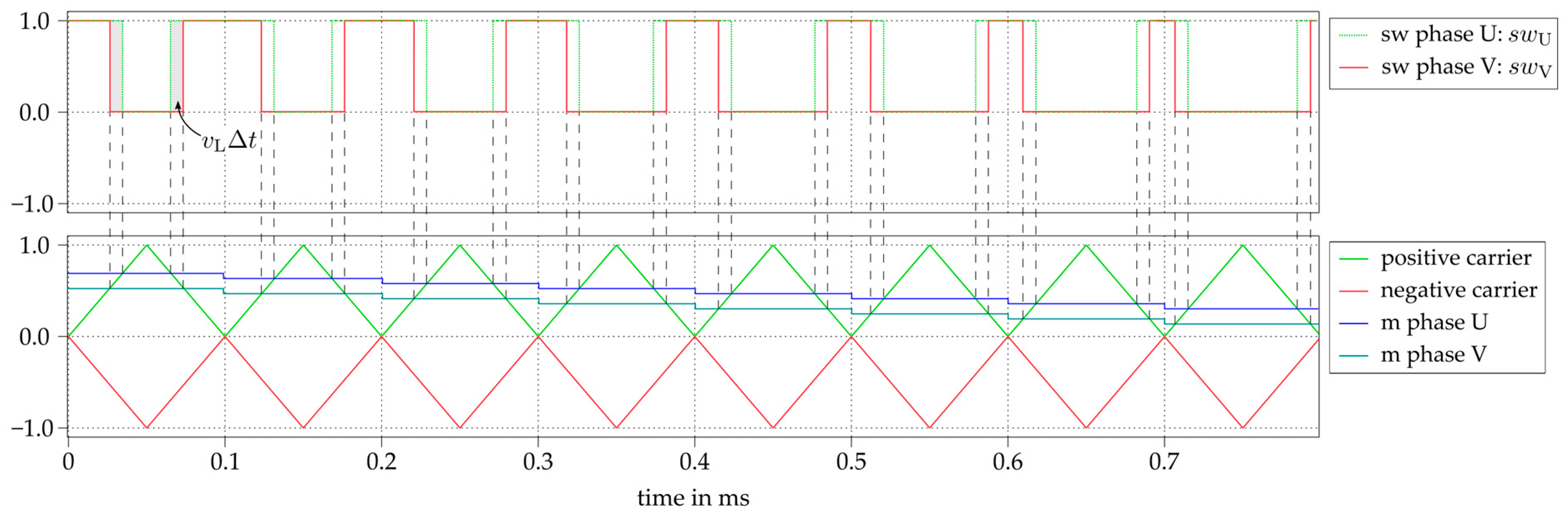
To describe the modulation scheme, it is clear from
Figure 1 that only a difference in the phase output voltages, which results in
which causes a current flow
. Furthermore, it is necessary to output phase voltages with different modulation degrees to be able to share the load current between all power semiconductors of a phase leg. For the constant current mode, the modulation degree is a sinusoidal function with a fundamental frequency of
, due to its intended use as a grid-connected inverter. A flipped carrier-based POD modulator was implemented, with the ability to offset the modulation index
for each phase in a very fine granularity. The shifting of
ultimately allows the adjustment of the voltage time area
(see
Figure 7) and thus the inductor current.
.
The switching signals for each transistor are derived from the corresponding phase switching signal
according to the following equations:
It is worth mentioning that an additional deadtime is added to each switching transition in order to prevent excessive stress for the transistors due to cross-commutation currents. A PI controller is placed in front of the modulator to generate the appropriate shift value so that the desired current is achieved in the load. During zero crossing of the modulation degree (), the switch-on times for the outer transistors become very short. As a result, during these transitions, the control margin drops to zero and the current cannot be controlled within the desired accuracy band. To mitigate this effect, a correspondingly large inductance should be used, as the current should be as constant as possible, with low ripple for the measurement of the total losses.
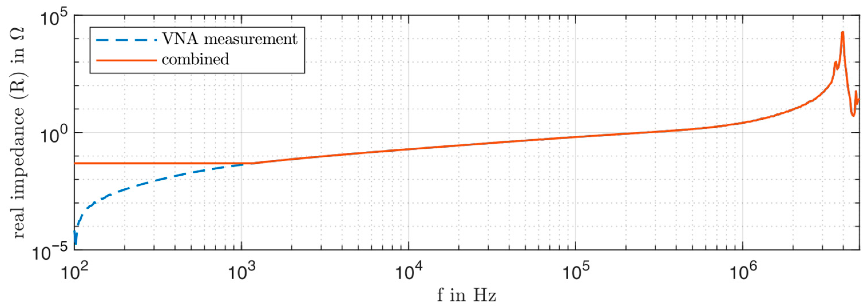
The inductor has another great importance for the OM measurements, because its losses need to be known very well for subtraction from the overall input power measured on the DC side. Air coils are best suited to get rid of any magnetic material losses, whose exact determination is very difficult. In this case, a toroid structure was used to guide the magnetic field within a predefined path with only a small amount of leakage. Accurately characterising the AC behaviour of the inductor, particularly measuring the real (ohmic) component, is of great importance. Therefore, a two-step combined approach was used: for lower frequencies, the DC resistance measured with a milliohmmeter is set, and for higher frequencies, the results from a VNA Bode 100 (OMICRON electronics GmbH, Klaus, Austria) with an external amplifier are used. This accounts for the situation where the VNA cannot measure the complex impedance for low frequencies as accurately as needed due to the lack of resolution, e.g., during estimation of the phase angle. The resulting impedance curve is depicted in
Figure 8, which highlights the lack of resolution in the lower frequency range.
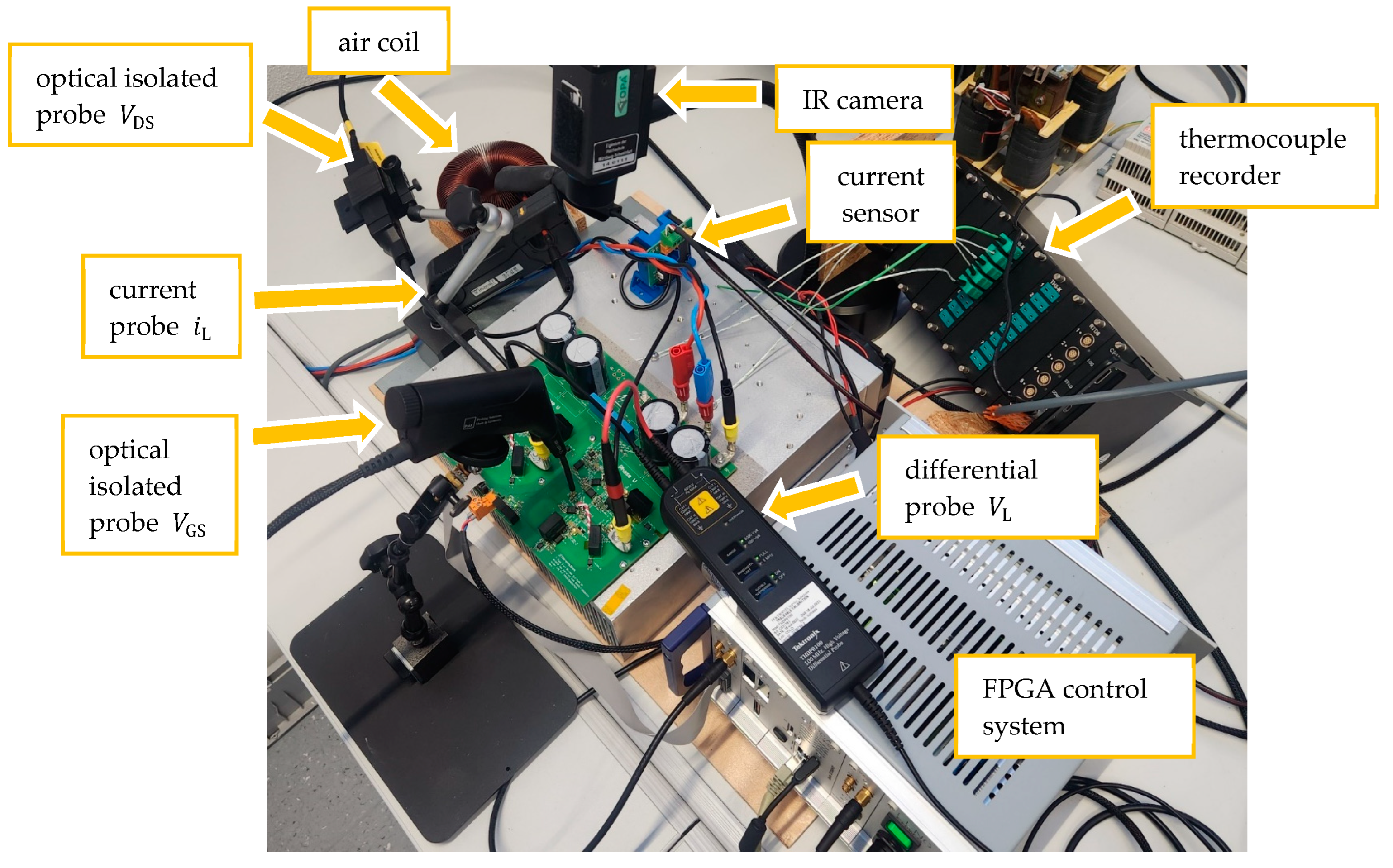
The laboratory setup is shown in
Figure 9. All modulation and control blocks are implemented in an FPGA control system, which can be operated from a GUI on a workstation. A zero-flux current probe with high bandwidth (10 MHz) is used for tracing the inductor current, which is necessary for post-processing the inductor losses. In contrast, a current sensor with lower bandwidth (100 kHz) is sufficient for the current control loop. For measurement of gate-source and drain-source voltages, optical isolated voltage probes with high CMRR were used to achieve clear waveforms with the lowest common mode noise. A precision power analyser, ZES Zimmer LMG670 (ZES ZIMMER Electronic Systems GmbH, Oberursel, Germany), was introduced into the DC supply lines to measure the losses on the DC side. A series of temperature sensors were also installed to continuously monitor the condition of the system, such as an even load sharing on the phase legs. With the proposed test setup, the operating temperature of the power transistors could be kept at a very constant level for all operating points to ensure minimal dependency on the
, which is known to be strongly temperature-dependent. This was accomplished by using a big heat sink with forced air cooling mounted on the top side of the cooled devices and measuring the heat sink temperature very close to the devices.
The setup also allows for open-loop operation of DPTs by just connecting the air coil differently and driving the gate signals appropriately. These measurements are essential to ascertain the optimum gate driver and deadtime adjustment. When using GaN HEMTs, the deadtime is very critical, as an extended deadtime can cause damage due to the high voltage drop () and associated losses. On the other hand, a very short deadtime can result in short circuits, leading to device damage. It is not possible to measure the drain currents in our setup, as inserting a sensor would increase the loop inductance and thus corrupt the results. Therefore, the voltage drop across the parallel GaN HEMTs was used to determine the dead time. As soon as shows an increase, measured at low currents, the transistor must therefore be actively switched on to conduct in the reverse direction.
4. Results
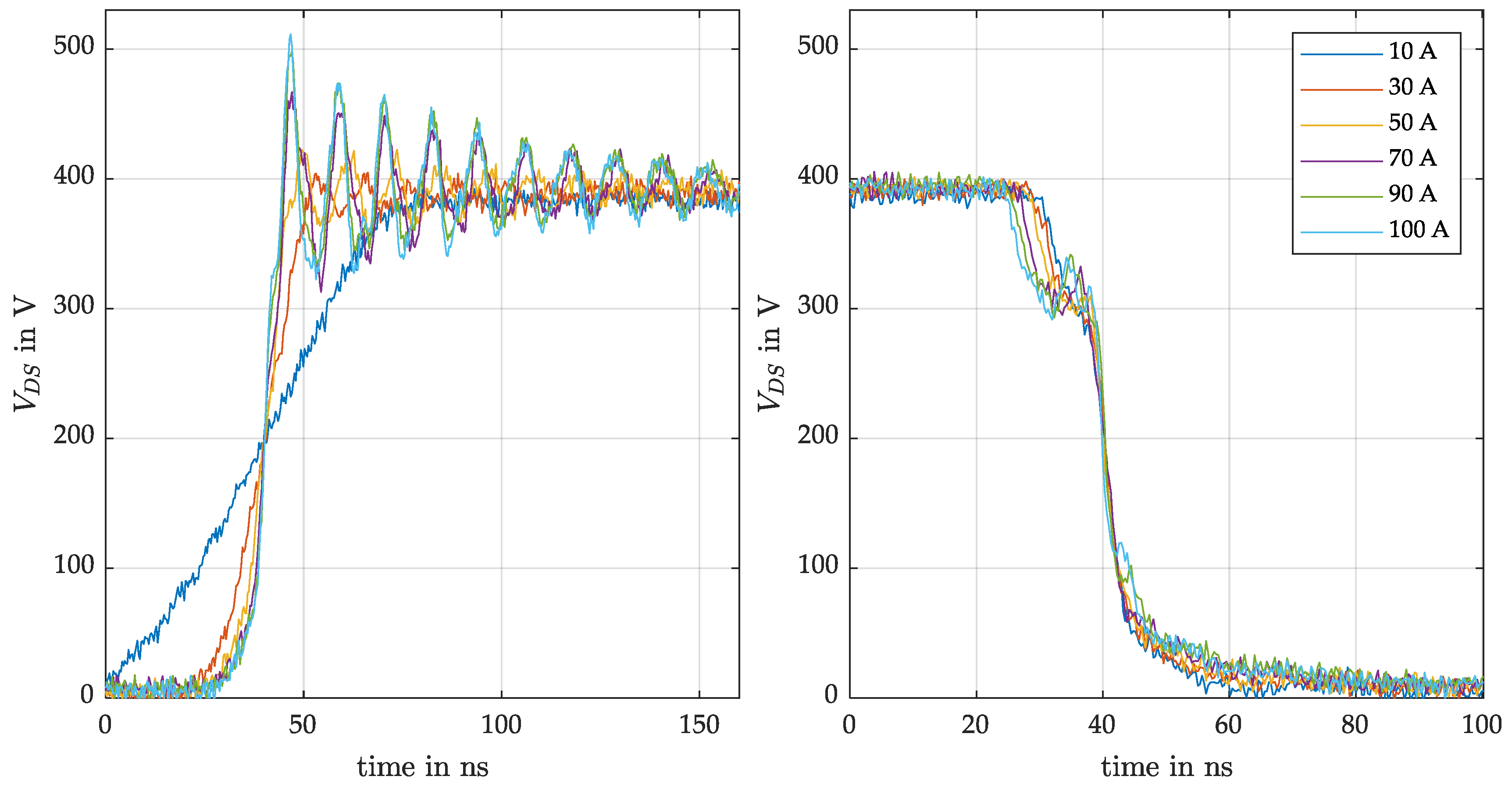
Figure 10 left shows the drain-source voltage at the turn-off event for different load currents. The overvoltage reaches a maximum of 500 V only at the maximum permissible current, indicating the low-inductance design of the switching loop. The turn-on waveforms (
Figure 10, right) also show a clean switching with the dip due to the loop inductance. An iterative series of measurements was carried out for all switches in the phase leg, to find an optimum for the gate control and to examine the switching characteristics. The results for switch U2 are shown as an example, although they do not differ significantly from the other switches.
Table 2 summarises the switching speeds, which are typically load current dependent for turn-off.
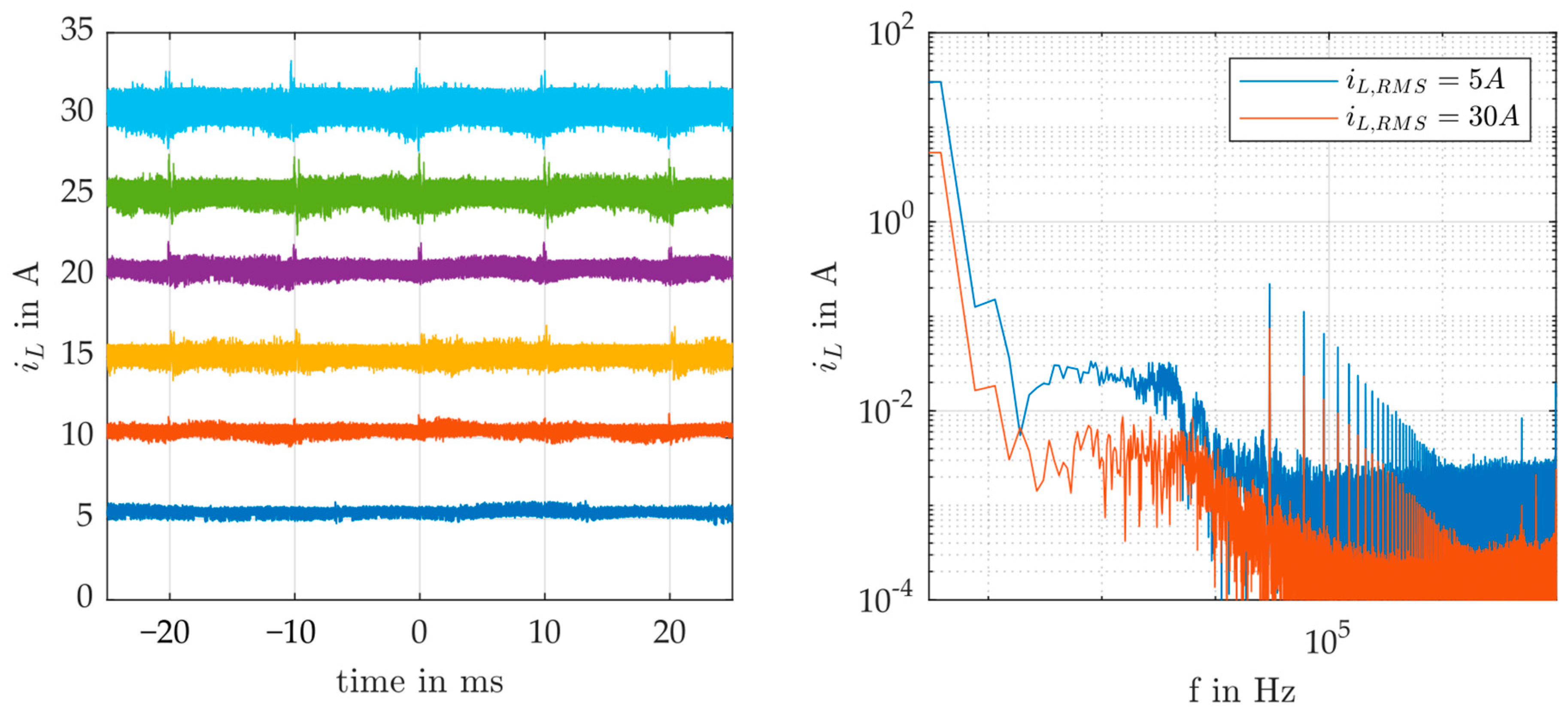
The curves in
Figure 11, left, represent the inductor current waveforms containing distortions during the zero crossing of the modulated voltage, which has a fundamental frequency of 50 Hz. For higher currents up to 30 A, the ripple increases to ±1 A, which introduces more distortions in the lower frequency range (100 Hz to 10 kHz), as could be seen in the right plot, which shows the representation of two selected currents in the frequency domain. With this outcome, one can obtain the inductor losses in conjunction with the inductor impedance (
Figure 8) and subtract them from the measured power on the DC input. Finally, a set of measurements for different currents and switching frequencies leads to the total inverter losses (for two-phase legs) depicted in
Figure 12. The curves show a clear dependence of the losses on the switching frequency, which was to be expected. The difference between 20 kHz and 30 kHz appears to be quite large compared to 30 kHz and 40 kHz. It can be assumed that switching losses are the root cause for the proportional big gap, as the
is constant due to the large heat sink and measured temperatures near the power devices. An extension of the OM measurements for AC currents would provide more precise findings, as this would allow the division of overall losses into the different loss mechanisms.
5. Discussion
This paper compares two methods for estimating stray inductances and validates them against measurements. The results show that accurately modelling the geometry of the PCB and components leads to a strong correlation between simulations and measurements. The simulation approach can be further enhanced by integrating the workflow presented in [
12] for parallel-connected GaN devices. This involves using SPICE simulations that incorporate a macromodel of the PCB—including all power and gate loop couplings—and a detailed model of the switching components. Time-domain simulation results can then be compared with measurements to validate the complete board model. By including time-domain waveforms, this approach enables thorough evaluation and optimisation of the design before PCB fabrication. This not only avoids costly redesigns but also improves PCB reliability and enhances the switching performance of the devices.
In the past, the DPT was standard for determining switching losses in Si and even SiC power semiconductors. This method involves measuring the voltage across the switch and the current through it. GaN HEMTs, on the other hand, can inherently switch very rapidly, achieving high current and voltage slew rates. As a result, parasitic inductances in the commutation loop must be minimised. This study presents a method for determining these inductances. This can help to further optimise the setup for achieving high performance. In a DPT, current measurement is challenging as it alters the commutation loop and introduces additional inductance. This added inductance can be of the same order of magnitude as the existing inductance, rendering the results of the double pulse test not directly applicable to the final application. The OM presented here offers an alternative to the DPT, providing greater accuracy in determining losses. As shown, the OM itself is not hard to implement even for a 3-level VSI, although the role of the inductor should not be underestimated. It can be seen from the two frequency responses (
Figure 8 and
Figure 11, right) that the losses in the inductor are essentially determined by the DC resp. very low frequency currents. The higher frequency components, e.g., at the switching frequency, fulfil a rather subordinate role. This underlines the importance of a precise resistance measurement for the lower frequencies.
6. Conclusions
For the characterisation and optimised operation of GaN transistors in VSIs, a multitude of techniques are required, which are summarised and highlighted in this paper. Power loop inductances, for example, play an important role in the optimised design process, since current transients become steeper with GaN-based technology. Occurring voltage overshoots limit the utilisation of the semiconductors. Hence, a small inductance is preferable. The presented methods show good compliance for estimating power loop inductances. Even the analytical calculation through dividing a PCB into several sections provides desirable results. This allows for the estimation of values quickly without any time-intensive simulations.
An important topic for characterising GaN transistors is the determination of losses. A conventional DPT does not produce accurate results, and the OM should be preferred. The described test bench is especially designed to investigate modules with different load currents while operating at nearly the same temperature. This allows a comparison of switching losses for similar operating conditions. However, it must be noted that such behaviour is not realistic in applications. Especially in highly integrated systems, the cooling power is limited. An extension of the OM for AC currents is essential for a deeper understanding, as this is the only method of breaking down the total losses, assigning them to the individual loss mechanisms and thus optimising the circuit in greater depth.
Combining all the measurements, simulations and calculations, the design and methodology represent an achievement for the design process of VSIs. This enables the optimisation of GaN layouts and pushes the technology to its limits.


