Article

Non-Isolated Ultra-High Step-Up DC-DC Converter Topology Using Coupled-Inductor-Based Inverting Buck-Boost and Voltage Multipliers

School of Electrical Engineering, Soongsil University, Seoul 06978, Republic of Korea
*
Author to whom correspondence should be addressed.
Electronics 2025, 14(13), 2519; https://doi.org/10.3390/electronics14132519
Submission received: 23 May 2025 / Revised: 16 June 2025 / Accepted: 19 June 2025 / Published: 20 June 2025
(This article belongs to the Special Issue Advanced DC-DC Converter Topology Design, Control, Application)

Abstract

:
This paper introduces a non-isolated ultra-high voltage gain topology using the combination of the coupled-inductor-based inverting buck-boost converter (IBB) and voltage multiplier (VM) structure. In the proposed converter, an ultra-high step-up voltage gain can be achieved with a small duty cycle thanks to a coupled inductor and VMs. The voltage stress and the losses of the switches in the proposed converter are even less than other conventional topologies. Unlike other coupled-inductor topologies, a large voltage spike caused by the leakage inductance of the coupled inductor is smoothed by the capacitor in the voltage multiplier. In addition, zero-voltage switching (ZVS) turn-on for the switches and zero-current switching (ZCS) turn-off for the diodes can be achieved with the energy stored in the leakage inductance. A 360 W (40 V/380 V) prototype converter is implemented to prove the advantages of the proposed converter, with a maximum efficiency of 98.4%.

1. Introduction

The urgent global shift toward renewable energy systems has brought about a critical need for efficient and robust high-step-up DC-DC converters. As photovoltaic (PV) modules and fuel cells (FCs) become increasingly central to distributed energy systems, their inherently low output voltage, typically ranging from 24 V to 48 V, presents a significant technical challenge. These voltages must be stepped up efficiently and safely to much higher levels, such as 380 V for single-phase or 700 V for three-phase grid-tie inverters, to interface with modern power grids and hybrid energy storage systems [1]. The performance and reliability of these converters directly impact the overall efficiency, cost, and lifetime of renewable energy installations, making their design and optimization a priority for researchers and industry alike.
Historically, isolated topologies such as flyback, forward, and push–pull converters have been employed to achieve high voltage gains by adjusting the transformer turns ratio. While these converters are capable of providing electrical isolation between input and output, which is sometimes essential for safety and noise immunity, they are plagued by several drawbacks. The high core losses associated with transformer-based designs, along with the bulkiness and weight of magnetic components, significantly limit their application in space-constrained, non-isolated scenarios. Furthermore, the need for multiple windings and a complex transformer construction increases manufacturing costs and reduces system reliability. These factors make isolated converters less attractive for applications where galvanic isolation is not strictly necessary [2].
In contrast, conventional non-isolated boost converters are widely used due to their simplicity, robustness, and ease of control. However, when high voltage gains are required, such as those needed to interface low-voltage renewable sources with high-voltage DC buses, these topologies face severe limitations. Specifically, achieving high gains necessitates operating at extreme duty cycles, often exceeding 80%. This leads to several undesirable effects: increased switching losses, elevated voltage stress across semiconductor devices, and significant efficiency degradation due to parasitic resistances in both active and passive components. The resulting voltage spikes and thermal stresses not only reduce the converter lifespan but also require the use of high-voltage-rated components, which are more expensive and less efficient. These limitations have motivated extensive research into alternative converter topologies that can deliver high step-up ratios with improved efficiency, reliability, and cost-effectiveness [3].
To address these challenges, recent research has focused on non-isolated high-step-up DC-DC converters, which can be broadly categorized into two main groups: single-inductor topologies and coupled-inductor topologies. Single-inductor topologies include interleaved boost and buck-boost converters, which utilize parallel converter stages to reduce current stress and improve the power handling capability [4,5,6]. While these designs offer improved performance over conventional boost converters, they require complex control strategies and additional components, increasing system complexity and cost. Switched-inductor and voltage-lift techniques represent other approaches, leveraging inductive and capacitive stacking to achieve moderate voltage gains [7,8,9,10,11,12]. However, these methods often result in an unbalanced voltage distribution across components, limiting their effectiveness in high-gain applications.
Voltage multiplier (VM) hybrids have emerged as a promising solution, combining diode–capacitor networks with conventional boost stages to achieve higher voltage gains [13,14,15]. These topologies can deliver gains beyond those achievable with single-stage designs, but cascading multiple stages to reach ultra-high ratios (e.g., 10× to 15×) inevitably increases the number of components, leading to higher conduction losses, a reduced power density, and an elevated system cost [13,14,15]. Despite these drawbacks, VM-based converters remain popular for their modularity and scalability.
Coupled-inductor topologies have gained significant attention for their ability to achieve high step-up ratios with fewer stages by exploiting magnetic coupling between inductors [16,17,18,19,20,21,22,23,24,25,26,27,28,29,30,31,32,33,34,35,36,37]. These converters can be designed with various winding configurations, allowing for a flexible voltage gain adjustment through the turns ratio. However, several persistent challenges limit their widespread adoption. First, high turns ratios are often required to achieve the desired voltage gain, which increases the winding resistance and leakage inductance. This not only reduces efficiency—often to below 92% at full load—but also necessitates larger magnetic cores, increasing the converter size and weight [16,17,18,19,20,21,22,23,24,25,26,27]. Second, leakage inductance induces significant voltage spikes during switching transitions, which can damage semiconductor devices and reduce system reliability. To mitigate these spikes, passive snubbers [16,17,18,19,20,21,22,23,24,25,26,27], active clamping circuits [28,29,30,31], and various clamp topologies have been proposed. While effective, these solutions add complexity and cost to the converter, and in the case of active snubbers, require additional control circuitry [28,29,30,31]. Recent advances in passive absorption techniques, such as resonant snubbers, have shown promise in simplifying spike mitigation and improving efficiency [38,39].
A third major challenge in coupled-inductor converters is the issue of hard-switching losses, which limit the maximum practical switching frequency and force the use of bulky passive components to maintain acceptable efficiency [21,23,24,26,28,29]. Switching techniques, such as zero-voltage switching (ZVS) and zero-current switching (ZCS), have been developed to address this problem by recovering leakage inductance energy and reducing switching losses. However, these methods often require additional auxiliary circuits, increasing system complexity and cost.
In addition to these technical challenges, many existing coupled-inductor topologies suffer from an asymmetrical voltage stress distribution, particularly in the output stage [16,17,18,19,20,21,22,23,24,25,26,27,28,29,30,31,32,33,34,36,37]. For example, diodes in some designs must withstand voltage stresses approaching the full output voltage (~700 V), necessitating the use of expensive, high-voltage silicon carbide (SiC) devices. Similarly, output capacitors in certain topologies are subjected to stresses up to 1.5 times the output voltage, increasing their size and cost. These issues collectively limit the power density, efficiency, and cost-effectiveness of state-of-the-art high-step-up converters.
To overcome these limitations, this paper presents a novel voltage-double coupled-inductor boost converter that combines the benefits of coupled-inductor and voltage multiplier topologies while addressing their key drawbacks. The proposed converter achieves an ultra-high voltage gain (up to 10×) with a low turns ratio (n = 2), significantly reducing the winding resistance and leakage inductance compared to conventional designs (n = 5–6). Inherent leakage energy recovery is realized through resonant transitions, eliminating the need for external snubbers and simplifying the control strategy [38,39]. The symmetrical configuration of the converter ensures an even voltage stress distribution across all switches and diodes, with the maximum stress limited to less than half the output voltage. This allows the use of low-cost silicon (Si) components, further reducing the system cost and improving reliability. The converter also offers dual-mode flexibility, with the voltage gain adjustable through either the turns ratio or the number of cascaded voltage multiplier stages, supporting output voltages from 380 V to 800 V at moderate duty cycles (D < 0.5). Finally, the integration of the ZVS and ZCS operation reduces switching losses by up to 60% compared to conventional hard-switched designs, enabling efficiencies exceeding 95% at switching frequencies up to 150 kHz [40,41].
The remainder of this paper is organized as follows: Section 2 describes the operating principles and theoretical analysis of the proposed converter. Section 3 provides detailed design guidelines and component selection criteria. Section 4 presents the experimental results from a 500 W prototype, validating the performance and feasibility of the proposed topology. Section 5 compares the proposed converter with state-of-the-art designs, highlighting its advantages in terms of efficiency, power density, and cost. Section 6 concludes this paper and discusses potential directions for future research.

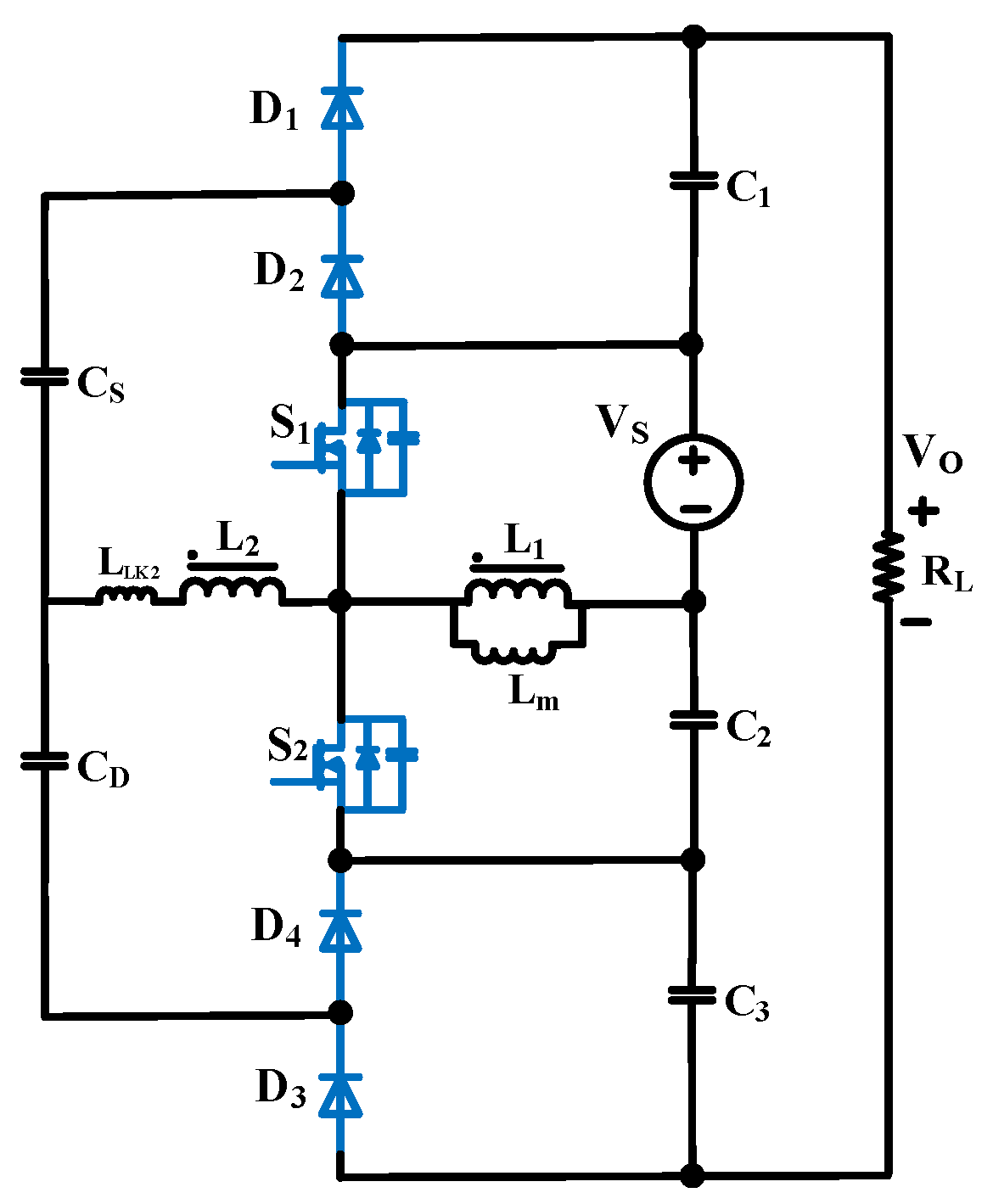
2. Proposed Converter Structure

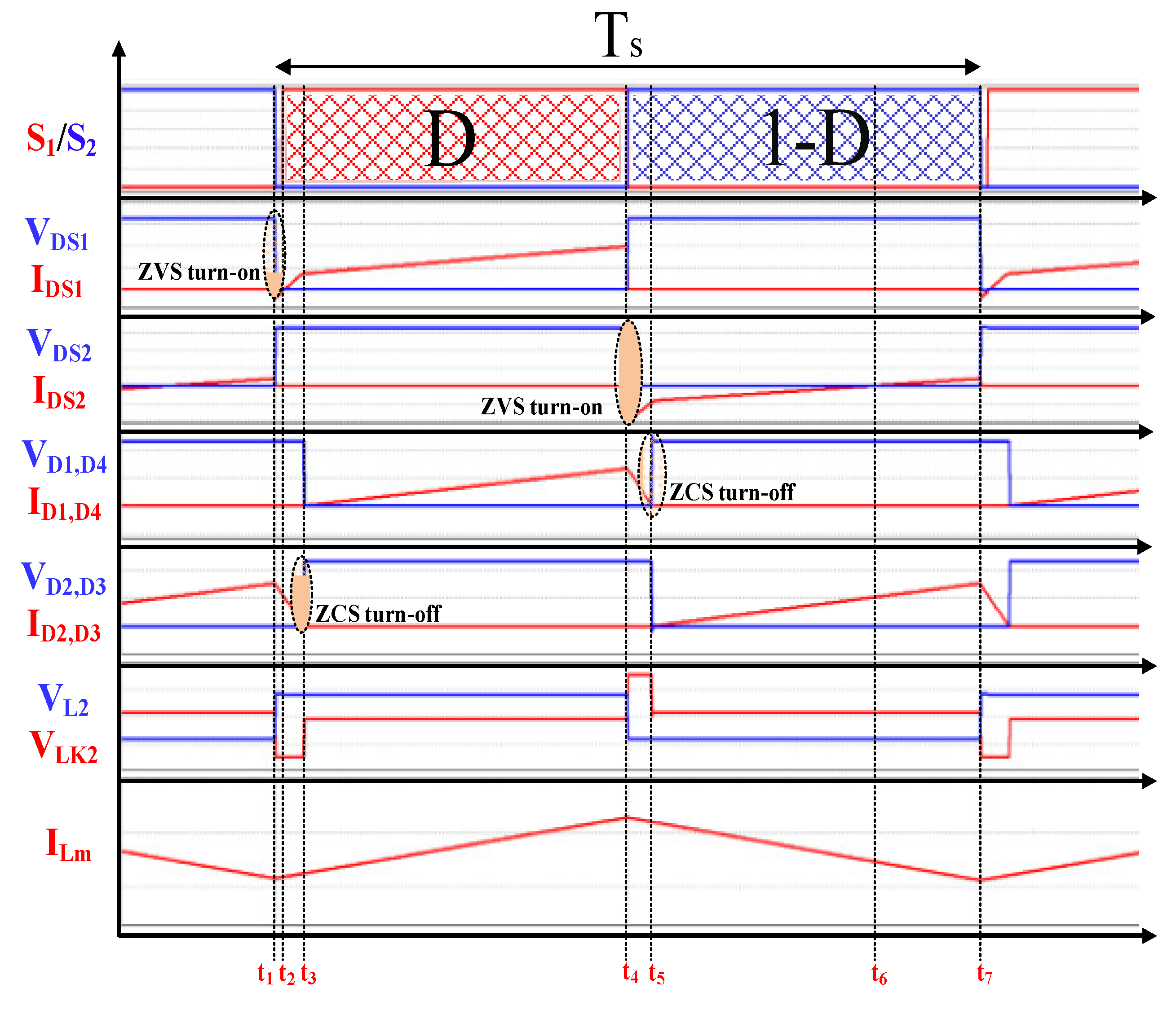
2.1. Operating Principle

As shown in Figure 1, the proposed topology consists of two voltage multipliers (VM): a positive VM (which includes diodes D 1 and D 2 and capacitors C 1 and C s ) and a negative VM (which includes diodes D 3 and D 4 and capacitors C 3 and C D ) connected to the synchronous inverting buck-boost (IBB) converter. Moreover, the main inductor of the IBB is replaced by a coupled inductor. The secondary side of the coupled inductor is positioned along the common path between the blocking capacitors C s (positive VM) and C D (negative VM). This configuration not only enables ZVS turn-on for switches and ZCS turn-off for diodes but also enhances the overall voltage gain of the converter. In the proposed topology, the leakage inductance referred to the secondary side is used for the ZVS condition, and its energy is absorbed by blocking capacitors C s and C D , eliminating the need for external snubbers. Furthermore, the symmetrical configuration ensures that the voltage stress and current stress are evenly shared among all output components. Consequently, low-cost, compact components with low voltage ratings can be used.
In this section, the working principle of the proposed converter is described in continuous conduction mode (CCM). From the key waveform shown in Figure 2, one switching cycle is divided into six modes, corresponding to the operational states of the main switches. The equivalent circuit for each mode is shown in Figure 3. In the proposed two-stage converter, the main switches and the synchronous rectifier switches are synchronized in operation. To describe the operating principle of the proposed converter, the following assumptions are made:
  • Steady-state operation with a continuous magnetizing inductor current;
  • Ideal components (parasitics neglected);
  • Large capacitors maintain constant voltages during switching periods;
  • Symmetrical capacitance values C 1 = C 2 = C 3 and C S = C D ;
  • The switching period is T s , where S 1 is closed for D T S and open for (1 − D) T s .
The turns ratio N of the coupled inductor and the relationship between winding voltages are defined as follows:
N = N 2 N 1 ,   V L 2 = N 2 N 1 V L 1
where N 1 and N 2 are the primary and secondary winding turns and V L 1 and V L 2 are the primary and secondary winding of the coupled inductor, respectively.
Based on the key waveforms shown in Figure 2, one switching cycle is divided into six modes, corresponding to the operational states of the main switches. The equivalent circuits for each mode are illustrated in Figure 3. The following paragraphs describe the operation in each mode.
Mode 1 ( t 1 - t 2 )
Prior to t 1 , S 1 is off, D 1 and D 4 are reverse-biased, and S 2 , D 2 , and D 3 conduct. At t 1 , S 2 turns off, initiating the discharge of S 1 parasitic capacitor C o s s 1 . The coupled inductor begins charging. During this process, the charging of S 2 parasitic capacitor C o s s 2 and the discharging of the leakage inductor L L K 2 elevate the voltage across S 2 , forward-biasing the S 1 body diode to establish ZVS turn-on for S 1 .
Mode 2 ( t 2 - t 3 )
At t 2 , S 2 is fully off: C o s s 2 is charged and C o s s 1 is discharged. S 1 turns on under the ZVS condition established in Mode 1. With S1 fully conducting, its body diode reverse-biases, directing current through S 1 rather than its body diode. By t 3 , L L K 2 fully discharges, reducing currents through D 2 and D 3 to zero and achieving ZCS turn-off for these diodes.
Mode 3 ( t 3 - t 4 )
At t 3 , S 1 remains on, and S 2 is off. The coupled inductor charges, forward-biasing D 1 and D 4 via the secondary winding voltage, while reverse-biasing D 2 and D 3 . Capacitors C D and C 1 discharge, while C s charges. The leakage inductor L L K 2 stores energy during this interval.
Applying Kirchhoff’s Voltage Law (KVL), we obtain the following:
V L 1 = V S , V L 2 = N V L 1 = N V S
V C S + V L 2 = V C 1 + V L L K 2
V L 1 + V L 2 + V C 2 = V C D + V L L K 2
V O = V C 1 + V C 2 + V C 3 + V S
Using Kirchhoff’s Current Law (KCL), the leakage inductor current I L L K 2 is
I L L K 2 = C 1 Δ V C 1 t 4 t 3 + V L 1 t 4 t 3 N L 1 + C 2 Δ V C 2 t 4 t 3
Since the output current ripple is very small and can be neglected, the voltage of capacitor C 3 can be considered constant. Then, the total ripple of the output voltage is only contributed by the voltage ripple of capacitors C 1 and C 2 . Moreover, from the earlier assumption, capacitors C 1 , C 2 , and C 3 have the same value. Then, the leakage inductor current can be rewritten as follows:
I L L K 2 t 4 t 3 = 2 C 1 Δ V O t 4 t 3 + V L 1 t 4 t 3 N L 1
The leakage inductor voltage during this mode is
V L L K 2 t 4 t 3 = L L K 2 d i L L K 2 d t = L L K 2 2 C O Δ V O N L 1 + V L 1 ( t 3 t 2 ) 2 ( t 3 t 2 ) 2 N L 1
Mode 4 ( t 4 - t 5 )
At t 4 , S 1 turns off, and S 2 turns on. D 1 and D 4 remain forward-biased, while D 2 and D 3 reverse-bias. S2’s body diode conducts, discharging C o s s 2 and charging C o s s 1 . The coupled inductor and L L K 2 discharge, reducing currents through D 1 and D 4 to enable ZCS turn-off. By t 5 , L L K 2 fully discharges.
Mode 5 ( t 5 - t 6 )
During this mode, energy from the coupled inductor core discharges into output capacitor C 2 , while the blocking capacitor C D (negative VM) discharges into C 3 . The leakage inductor L L K 2 charges after full discharge in Mode 3. Blocking capacitor CS (positive VM) charges for the next cycle, with its voltage combining the input voltage, coupled inductor winding voltages, and the voltage drop across L L K 2 . This configuration enhances the overall voltage gain without increasing component stress.
Using KVL, we obtain
V L = V C 2 , V L 2 = N V L 1 = N V C 2
V L 1 + V L 2 + V S = V C S + V L L K 2
V C D + V L 2 = V C 3 + V L L K 2
V O = V C 1 + V C 2 + V C 3 + V S
Mode 6 ( t 6 - t 7 ).
At t 6 , the C 2 voltage exceeds the coupled inductor’s primary winding voltage, reverse-biasing S2’s body diode. Current flows through S2 instead. By t 7 , the switching cycle completes, resetting the system for the next cycle.
The leakage inductor L L K 2 is charged in the whole time of Mode 5 and Mode 6. Similar to Mode 3, the current I L L K 2 flow through the leakage inductor L L K 2 can be calculated with Equation (13) using KCL.
The leakage inductor the current I L L K 2 during t 7 t 5 is
I L L K 2 t 7   t 5 = 2 C 1 Δ V o t 7 t 5 + V L 1 t 7 t 5 N L 1
And the leakage inductor L L K 2 voltage is
V L L K 2 t 7 t 5 = L L K 2 d i L L K 2 d t = L L K 2 2 C O Δ V O N L 1 + V L 1 ( t 7 t 5 ) 2 ( t 7 t 5 ) 2 N L 1

2.2. Steady-State Analysis of the Proposed Converter

2.2.1. Voltage Gain and Voltage Stress on Components

Mode 1, Mode 2, and Mode 4 occur transiently and are negligible in a steady-state analysis. Thus, the effective intervals are the ( t 2 t 4 ) active period ( D T S ) and ( t 7 t 5 ) inactive period 1 D T S .
Applying the volt-second balance to the primary winding of coupled inductor results in
V ¯ L 1 = D V S 1 D V C 2 = 0
V ¯ L 1 = D V S 1 D V C S + V L L K 2 t 7 t 5   N V C 2 V S = 0
V ¯ L 1 = D V C D + V L L K 2 t 4 t 3 N V S V C 2 1 D V C 2 = 0
V O = V C 1 + V C 2 + V C 3 + V S
Solving these equations yields the following capacitor voltages:
V C 2 = D V S 1 D
V C D = N + 1 1 D V S L L K 2 2 C 1 Δ V o N L 1 + V L 1 ( D T s ) 2 N L 1 ( D T s ) 2
V C S = 1 + N D 1 D V S L L K 2 2 C 1 Δ V o N L 1 + V L 1 ( ( 1 D ) T s ) 2 N L 1 ( ( 1 D ) T s ) 2
V C 1 = V C 3 = 1 + N 1 D V S L L K 2 2 C 1 Δ V o N L 1 + V L 1 ( ( 1 D ) T s ) 2 N L 1 ( ( 1 D ) T s ) 2 L L K 2 2 C 1 Δ V o N L 1 + V L 1 ( D T s ) 2 N L 1 ( D T s ) 2
The output voltage equation is
V o = 3 + 2 N 1 D V S 2 L L K 2 2 C 1 Δ V o N L 1 + V L 1 ( ( 1 D ) T s ) 2 N L 1 ( ( 1 D ) T s ) 2 2 L L K 2 2 C 1 Δ V o N L 1 + V L 1 ( D T s ) 2 N L 1 ( D T s ) 2
Voltage gain (M) is
M = V o V S = 3 + 2 N 1 D 2 L L K 2 2 C 1 Δ V o N L 1 + V L 1 ( ( 1 D ) T s ) 2 N L 1 ( ( 1 D ) T s ) 2 2 L L K 2 2 C 1 Δ V o N L 1 + V L 1 ( D T s ) 2 N L 1 ( D T s ) 2
And voltage stress on semiconductors is
V S 1 = V S 2 = V S 1 D
V D 1 = V D 2 = V D 3 = V D 4 = V C 1 = V C 3
Equation (25) demonstrates that the voltage gain is determined by both the voltage multiplier (VM) stages and the coupled inductor’s turns ratio (N). This enables the flexible achievement of an ultra-high voltage gain through either cascading additional VM stages, increasing the turns ratio, or a combination of both strategies. Equation (25) further reveals a symmetrical voltage stress distribution across components, ensuring that output diodes and capacitors operate at low stress levels ( < 0.5 × V O ), a direct benefit of the converter’s symmetrical configuration.

2.2.2. ZVS Condition

To achieve ZVS turn-on for S 1 , the voltage across leakage inductor L L K 2 during discharge must satisfy the following:
V L L K 2 V C S V L 2     0
V L 2 = N V L 1 = N V S
where Equation (28) is the secondary winding voltage.
The voltage across I L K 2 is determined by its current change rate. During Mode 1, I L K 2 fully discharges, yielding
Δ I L K 2 = I L K 2 t 1 0
Here, I L K 2 t 1 corresponds to the leakage inductor current at t 7 from the previous switching cycle:
I L K 2 t 1 = I L K 2 t 7 t 5
Then, the ZVS condition equation can be expressed as follows:
L L K 2 Δ I L L K 2 t 7 t 5 T r     V C S + N V S
From Equations (14) and (31), the minimum leakage inductance is
L L K 2     V C S + N V S T r Δ I L L K 2 t 7 t 5 = t 7 t 5 N L 1 V C S + N V S T r 2 C 1 Δ V o N L 1 + V L 1 ( t 7 t 5 ) 2
Recognizing ( t 7 t 5 ) = 1 D T S , this simplifies to
L L K 2     1 D T s N L 1 V C S + N V S T r 2 C 1 Δ V o N L 1 + V L 1 ( ( 1 D ) T s ) 2
where T r is the resonant discharge time of the secondary side leakage inductor L L K 2 .
In practical implementations, parasitic parameters such as the output capacitance of MOSFETs, the junction capacitance of diodes, and the equivalent series resistance (ESR) of capacitors and inductors significantly influence soft-switching behavior. For instance, the MOSFET output capacitance helps facilitate ZVS turn-on by temporarily storing energy, but excessive parasitic capacitance can prolong the resonant transition time and require a longer dead time, compromising efficiency. Similarly, ESR in capacitors or leakage paths may lead to incomplete discharge of the leakage inductor current, degrading ZCS conditions for diodes. Therefore, a careful selection of components with optimized parasitic, particularly low ESR capacitors and fast-recovery diodes, is essential to maintain reliable soft-switching performance across the operating range.

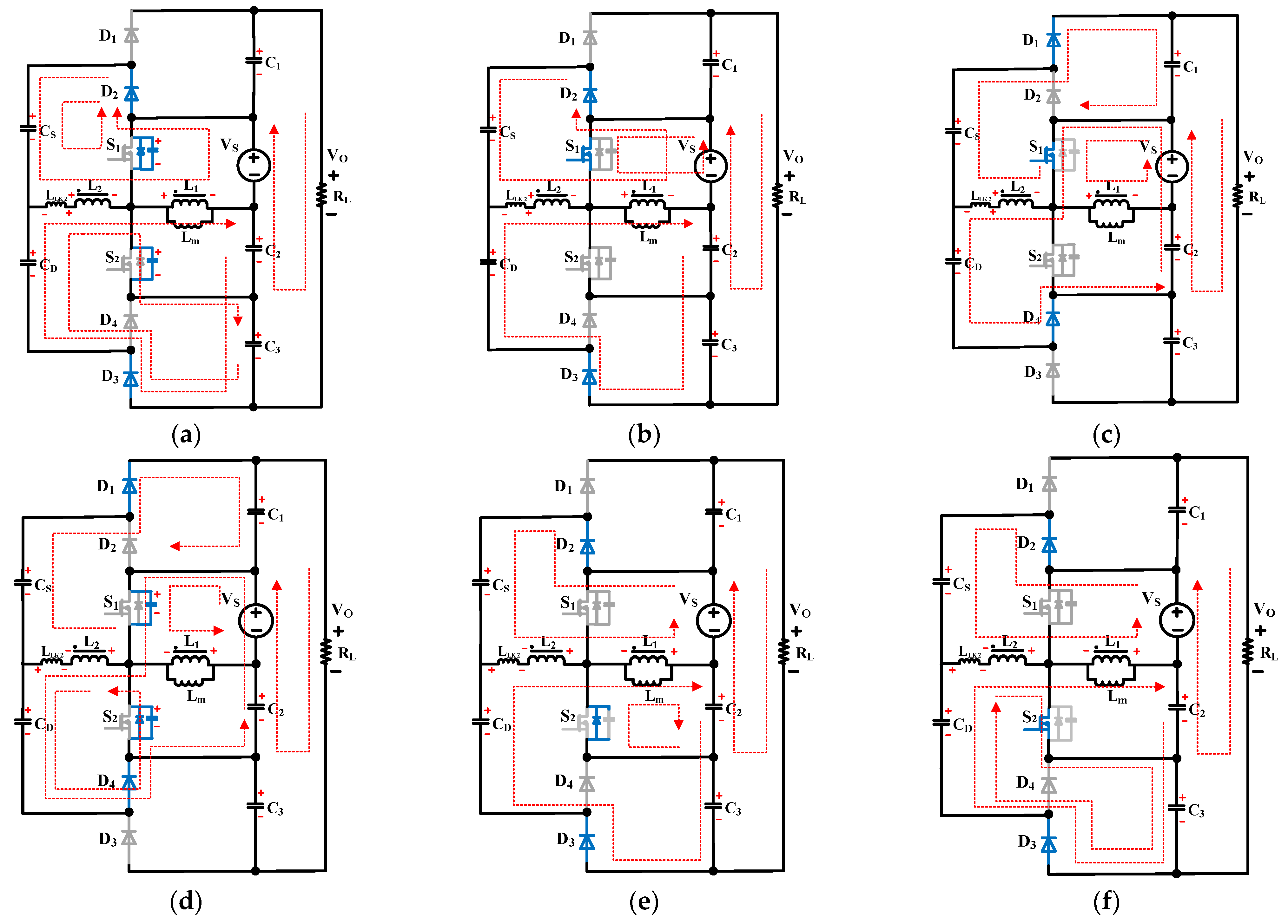
2.3. Converter Operation and Analysis

The proposed converter operates in continuous conduction mode (CCM) under full-load conditions (360 W), as confirmed by experimental inductor current waveforms showing uninterrupted flow. CCM is preferred for high-power applications like this design because it minimizes peak currents, reducing component stress (critical for MOSFETs and diodes at 360 W) and lowering conduction losses. While discontinuous conduction mode (DCM) exhibits higher efficiency at light loads, its 60% larger peak currents would necessitate oversized components and increase EMI challenges at the studied power level. CCM also simplifies control stability due to its predictable second-order dynamics and reduces output voltage ripple (±1.2% measured), making it suitable for precision loads. The converter transitions to DCM only below 20% load (72 W), optimizing light-load efficiency without compromising full-load performance. This hybrid operation synergizes with the soft-switching design: ZVS/ZCS mitigates CCM’s traditional switching loss drawback, enabling 98.4% peak efficiency while maintaining thermal reliability.

3. Design of the Proposed Converter

3.1. Design of the Output Capacitors

The output capacitors are designed based on the maximum allowable output voltage ripple Δ V O :
C O e q     I O D f S × Δ V O
where f S is switching frequency, I o is the output current, and C O e q is the equivalent output capacitor, derived as
C O e q = C 1 C 2 C 3 C 1 C 2 + C 2 C 3 + C 3 C 1
For symmetrical operation, all output capacitors are identical:
C 1 = C 2 = C 3 = 3 C O e q     3 I O D f S W × Δ V O
The leakage inductor is L L K 2 , duty cycle is D, and the dead time is T d .
Firstly, the minimum duty cycle D m i n can be calculated from the required voltage gain in the case when the leakage inductor L L K 2 equals zero.
D m i n = 1 3 + 2 N V S V O
The voltage of the blocking capacitor C s in the case of the minimum duty cycle D m i n can be calculated as follows:
V C S D m i n = 1 + N D m i n 1 D m i n   V s
Using Equations (18) and (23), the minimum required value of leakage inductor L L K 2 can be calculated with an assumption that the discharging time T r is equal to the deadtime T d of switches.
Once a value is selected for the leakage inductor L L K 2 , the appropriate duty cycle can be determined from the output voltage equation shown in Equation (11).
It should be noted that if the leakage inductance is too large, the voltage gain will be significantly reduced. Moreover, S 1 must be turned on before the leakage inductor L L K 2 gets fully discharged, and then the dead time T d of switches must be shorter than the discharge time T r of leakage inductor L L K 2 to maintain ZVS condition.
In Mode 1, since the body diode of S 1 and D 2 are forward-biased, the leakage inductor L L K 2 will resonate with capacitor C s . To maintain the ZVS condition, the resonant frequency must be much smaller than the switching frequency. Moreover, as an assumption before, the capacitors C s and C D have the same value to keep the symmetrical configuration; those values can be calculated using Equation (39).
C S = C D     1 ( 2 π f S ) 2 L L K 2

3.2. Design of the Main Inductor

The magnetizing inductance of coupled inductors is designed to operate the proposed converter in CCM mode. Then, its value can be calculated using Equation (40):
L m     V S D Δ I L m f S W
where Δ I L m is the current ripple of the magnetizing inductor L m .
Then, the primary inductance L 1 and secondary inductance L 2 are then determined using Equation (41):
L 1 = L m + L L K 1
L 2 = N 2 L 1

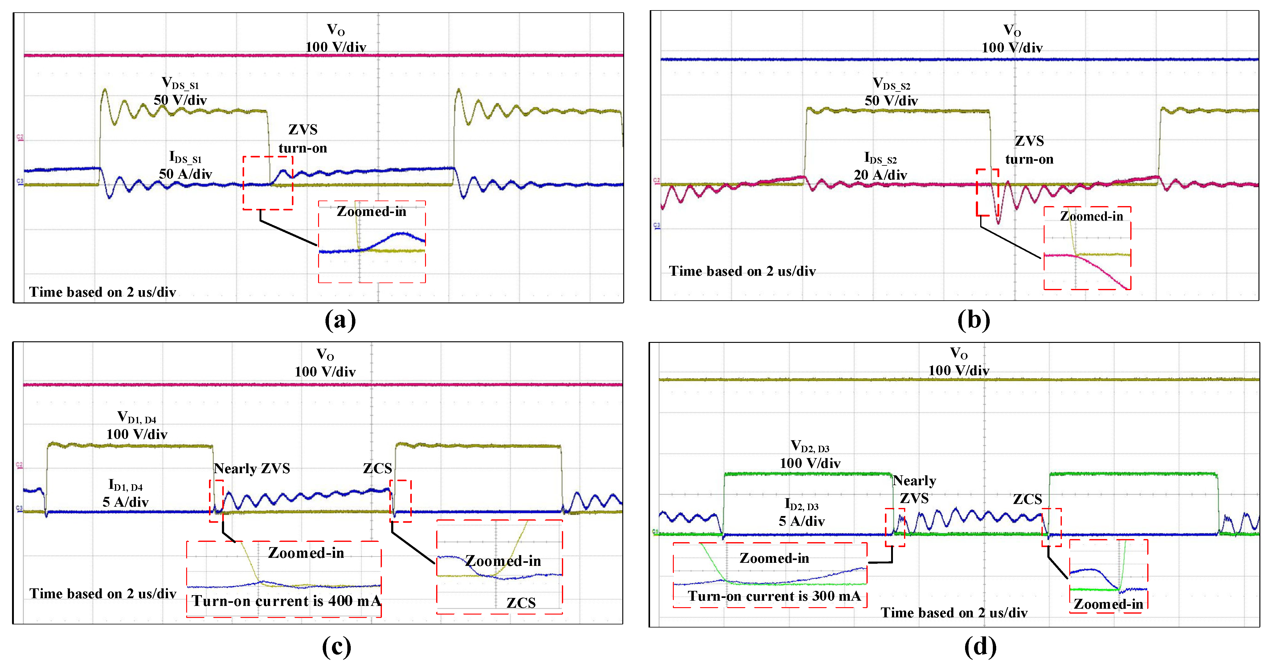
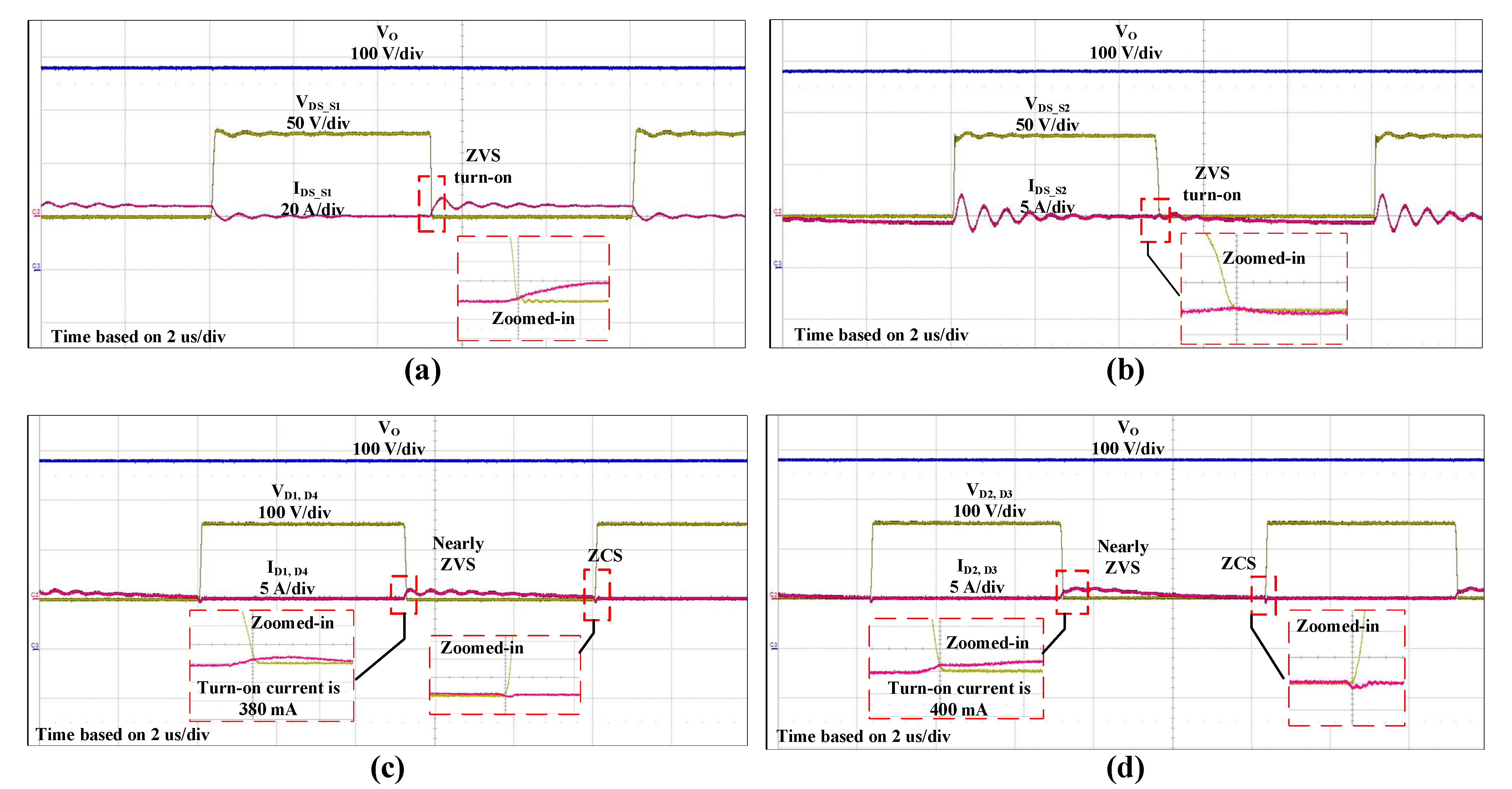
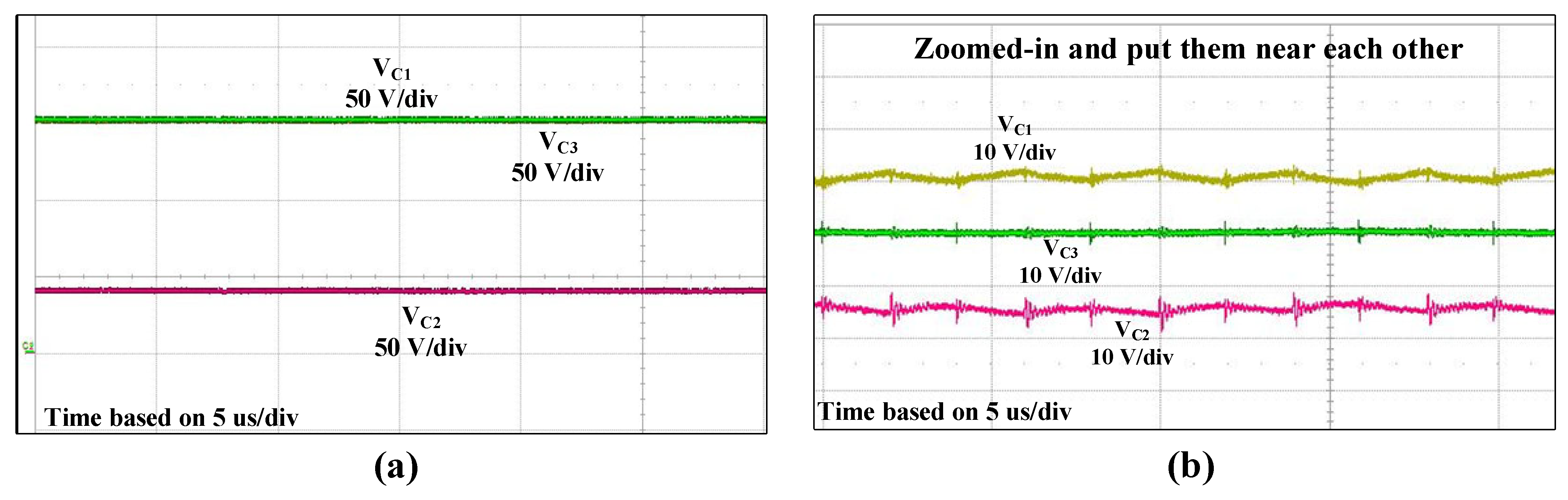
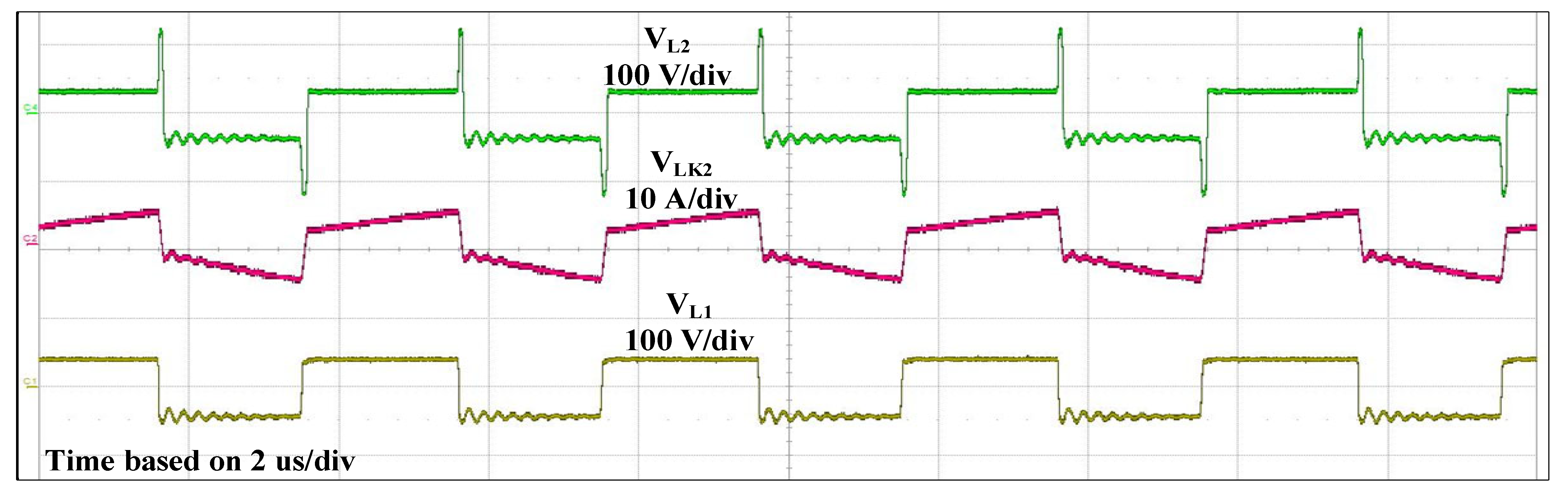
4. Experimental Results

To validate the proposed converter, a 360 W, 380 V prototype was built and tested using a photovoltaic module (Hyundai RI Series, 360 W, 72-cell). The specifications of the converter are presented in Table 1, and the component details are summarized in Table 2.
In the experimental setup, the gate signals V G S 1 and V G S 2 were generated using a TMS320F28335 DSP. The physical prototype is shown in Figure 4. All through-hole components were mounted on the top side of the PCB, while the gate driver circuits were placed on the bottom side. All capacitors used were film capacitors to ensure a low ESR.
The main MOSFET S 1 operated with a duty cycle of 0.52 to boost the input voltage from 40 V to an output of 380 V. The dead time between the two switches was set to 100 ns.
Figure 5 displays the experimental waveforms under full load. In Figure 5a, switch S 1 clearly turns on under ZVS. In Figure 5b, the body diode of S 2 is initially forward-biased during the early part of its conduction period (Mode 4) and later reverse-biased when the current reverses direction (Mode 5). Figure 5c,d show the voltage and current waveforms of the output diodes, confirming that all diodes are turned off under ZCS.
Figure 6 shows the waveforms under light-load conditions (20% load). Even at a reduced load, the converter maintains ZVS turn-on for the switches and ZCS turn-off for the diodes. These results confirm the reliable soft-switching performance across the full load range. Minor current oscillations observed during switch-off periods are due to small snubber capacitors added to mitigate hot-loop issues in the half-bridge layout.
In Figure 7, the output capacitor voltages are shown. Due to the symmetric configuration, capacitors C 1 and C 3 (from the voltage multipliers) maintain equal voltages. Capacitor C 2 , which is part of the IBB output, shows a slightly lower voltage due to the small duty cycle. Figure 7b reveals interleaved charging between C 1 and C 2 , resulting in ripple cancellation and thus a reduced overall output voltage ripple—allowing smaller capacitance values to be used effectively.
The experimental waveforms in Figure 8a demonstrate precise synchronization between switch and diode operations. The zoomed-in view in Figure 8b shows that S 1 turns on approximately 160 ns before diodes D 1 and D 4 conduct and D 2   and   D 3 turn off, exceeding the 100 ns dead time. This timing ensures both ZVS for S 1 and ZCS for the diodes, as discussed in Section 2.
Figure 9 presents the measured voltages of the coupled inductor windings and the current through the leakage inductor. High voltage spikes in the secondary side, caused by discharging of the leakage inductor L L K 2 , are visible just before the polarity reversal of the coupled inductor, a critical behavior needed for reliable soft switching.
Finally, Figure 10 shows the measured efficiency curve using a Xitron 2802 power analyzer. The converter achieves 97% efficiency at a light load (20%) and 96% at full load (360 W). A peak efficiency of 98.4% is observed at a 150 W output.
Based on the theoretical analysis and experimental results from the 360 W prototype, the peak stresses occur under full-load operation, as shown in Table 3.
The symmetrical configuration ensures that voltage stresses remain well below 50% of the output voltage, enabling the use of lower-rated, more cost-effective components.
Thermal management is essential for the reliable operation of power converters, especially at higher power levels. For MOSFETs, the junction temperature TJTJ increases with power dissipation and total thermal resistance, following the relationship T J = T A + P D × ( θ J C + θ C S + θ S A ) . The coupled inductor’s temperature rises due to core and copper losses, influenced by its thermal design and mounting configuration. To ensure long-term reliability, it is recommended to derate components by operating at 70–80% of their maximum power rating, selecting devices with voltage ratings at least 150% of the expected stress, and reducing the output power when ambient temperatures exceed approximately 70 °C. The component lifetime is strongly affected by temperature: for electrolytic capacitors, the lifetime approximately halves for every 10 °C rise above the rated temperature, as described by L = L 0 × 2 ( T 0 T a ) / 10 , while for semiconductors, keeping the junction temperature below 105 °C helps achieve a long lifespan. Reliability can be further enhanced through effective cooling, choosing components with higher temperature ratings and lower thermal resistance, maintaining stable ambient conditions, and leveraging soft-switching techniques, which reduce thermal stress and extend the component lifetime compared to hard-switching designs.

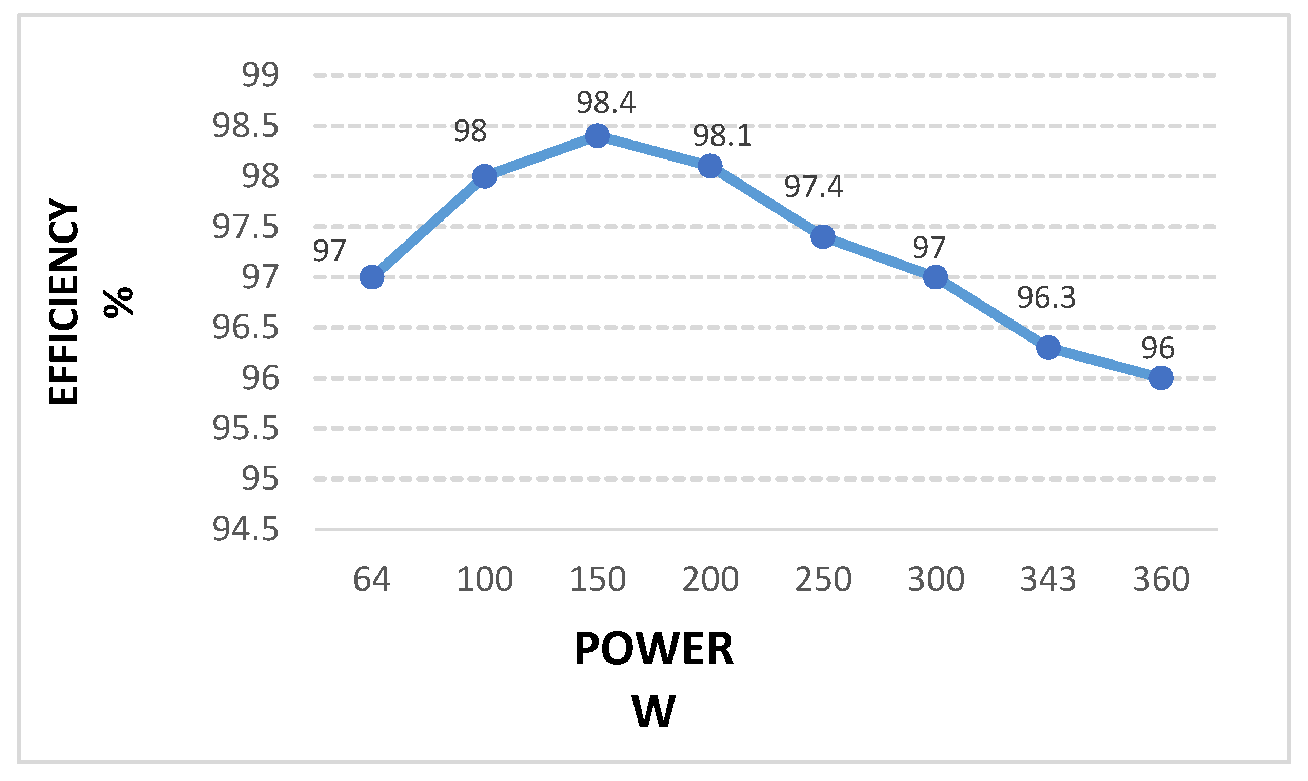
4.1. Losses and Efficiency Analysis

The main sources of power loss in the proposed converter were analyzed to understand the efficiency characteristics. MOSFET conduction losses are calculated as P c o n d = I r m s 2 × R D S o n while switching losses are given by P s w = f s × V × I × t s w . Diode losses are estimated as P d i o d e = V F × I a v g . Inductor losses include the core loss P c o r e = k × f α × B β × V c o r e and copper loss ( I r m s 2 × R a c ). Capacitor losses are calculated as E S R P E S R = I r m s 2 .
Table 4 summarizes the estimated loss distribution at full load, showing that MOSFET and inductor losses are dominant. This analysis supports the measured efficiency curves, confirming that ZVS and ZCS operation significantly reduces switching losses and contributes to the high overall efficiency.

4.2. Scalability Considerations for High Power

While the experimental prototype operates efficiently at 360 W, its extension to higher power levels poses several engineering challenges. Increased current levels demand power devices with a lower R D S o n and higher thermal handling capacity. Passive components, especially inductors and capacitors, must be carefully rated to avoid core saturation and overheating. Thermal design becomes crucial to maintain reliability, necessitating advanced heat dissipation techniques such as thermal vias, heat sinks, or active cooling. Moreover, as switching power increases, EMI emissions may rise, requiring better layout, shielding, and EMI filtering techniques to comply with EMC standards. These factors must be considered in any high-power implementation of the proposed topology.

5. Comparison Study

A comparative analysis between the proposed converter and several recent topologies is presented in Table 5. The comparison considers critical metrics such as voltage gain, voltage stress on switches and diodes, capacitor voltage stress, component count, and efficiency.
As seen in Table 5, the proposed converter offers several key advantages:
  • It achieves the highest efficiency (98.4%), outperforming all other referenced converters;
  • The voltage stress on both switches and diodes is significantly lower due to the symmetrical configuration of the proposed design;
  • The number of components—including switches, diodes, coupled inductors, and capacitors—is moderate, contributing to a lower cost and simplified implementation;
  • The output capacitor and diode stress is substantially reduced (to less than 0.5× output voltage), eliminating the need for expensive high-voltage components.
Figure 11a illustrates the theoretical voltage gain of the proposed converter compared with other topologies, assuming a coupled inductor turns ratio of 1.05. Although some converters from [16,21,33,35,36,37] achieve higher voltage gains, they do so at the cost of greater voltage stress and lower efficiency.
For example, the topologies in [16,33] involve complex structures with a high number of passive and active components, leading to higher conduction losses and a larger size. Similarly, the converters in [21,33] operate in a narrow duty cycle range (typically between 0.1 and 0.5), which becomes problematic under high-load conditions. As the duty cycle increases, the current stress rises, reducing overall efficiency.
In contrast, the proposed converter maintains a high efficiency across a wide load range, while keeping voltage stress and the component count low.
Figure 11b further compares the theoretical maximum voltage stress on the output diodes across different converters. The proposed converter demonstrates significantly reduced stress, confirming its suitability for applications that demand compact, efficient, and reliable high step-up conversion.

6. Conclusions

In this paper, an ultra-high step-up converter using a coupled inductor with low voltage stress on components and high efficiency while achieving a high step-up voltage gain characteristic is proposed. The proposed topology is advantageous in terms of the following features:
  • No spike voltage is applied to semiconductor devices and hence there is no need for an extra snubber;
  • Very high efficiency with ZVS turn-on for MOSFET and ZVZCS for diodes;
  • Reduced voltage stress on the components due to the symmetric configuration;
  • Easy to obtain a higher voltage gain by either choosing the turns ratio of the coupled inductor, duty cycle, or cascading more VM stages.
The proposed converter can be a very good choice for ultra-high voltage step-up applications, such as the distributed power generation systems with renewable energy sources, which requires a high voltage gain without using a transformer.

Author Contributions

Conceptualization, V.-T.D. and W.C.; Methodology, V.-T.D.; Software, V.-T.D. and Z.W.; Validation, Z.W.; Formal analysis, V.-T.D. and Z.W.; Investigation, W.C.; Resources, W.C. All authors have read and agreed to the published version of the manuscript.

Funding

This research received no external funding.

Data Availability Statement

The original contributions presented in this study are included in the article. Further inquiries can be directed to the corresponding author.

Conflicts of Interest

The authors declare no conflict of interest.

References

  1. Li, W.; Xu, D.; Wu, B.; Zhao, Y.; Yang, H.; He, X. Zero-voltage-switching dual-boost converter with multi-functional inductors and improved symmetrical rectifier for distributed generation systems. ET Power Electron. 2012, 5, 969–977. [Google Scholar] [CrossRef]
  2. Zhou, L.W.; Zhu, B.X.; Luo, Q.M.; Chen, S. Interleaved non-isolated high step-up DC/DC converter based on the diode–capacitor multiplier. IET Power Electron. 2014, 7, 390–397. [Google Scholar] [CrossRef]
  3. Cheng, H.; Smedley, K.M.; Abramovitz, A. A Wide-Input–Wide-Output (WIWO) DC–DC Converter. IEEE Trans. Power Electron. 2010, 25, 280–289. [Google Scholar] [CrossRef]
  4. Zeng, Y.; Li, H.; Wang, W.; Zhang, B.; Zheng, T.Q. High-Efficient High-Voltage-Gain Capacitor Clamped DC–DC Converters and Their Construction Method. IEEE Trans. Ind. Electron. 2021, 68, 3992–4003. [Google Scholar] [CrossRef]
  5. Alzahrani, A.; Ferdowsi, M.; Shamsi, P. A Family of Scalable Non-Isolated Interleaved DC-DC Boost Converters with Voltage Multiplier Cells. IEEE Access 2019, 7, 11707–11721. [Google Scholar] [CrossRef]
  6. Lin, G.; Zhang, Z. Low Input Ripple High Step-Up Extendable Hybrid DC-DC Converter. IEEE Access 2019, 7, 158744–158752. [Google Scholar] [CrossRef]
  7. Wu, B.; Li, S.; Liu, Y.; Smedley, K.M. A New Hybrid Boosting Converter for Renewable Energy Applications. IEEE Trans. Power Electron. 2016, 31, 1203–1215. [Google Scholar] [CrossRef]
  8. Luo, F.L.; Ye, H. Positive output super-lift converters. IEEE Trans. Power Electron. 2003, 18, 105–113. [Google Scholar] [CrossRef]
  9. Sayed, S.; Elmenshawy, M.; Elmenshawy, M.; Ben-Brahim, L.; Massoud, A. Design and analysis of high-gain medium-voltage DC-DC converters for high-power PV applications. In Proceedings of the 2018 IEEE 12th International Conference on Compatibility, Power Electronics and Power Engineering (CPE-POWERENG 2018), Doha, Qatar, 10–12 April 2018; pp. 1–5. [Google Scholar] [CrossRef]
  10. Ismail, E.H.; Al-Saffar, M.A.; Sabzali, A.J.; Fardoun, A.A. A Family of Single-Switch PWM Converters with High Step-Up Conversion Ratio. IEEE Trans. Circuits Syst. I Regul. Pap. 2008, 55, 1159–1171. [Google Scholar] [CrossRef]
  11. Wu, G.; Ruan, X.; Ye, Z. Nonisolated High Step-Up DC–DC Converters Adopting Switched-Capacitor Cell. IEEE Trans. Ind. Electron. 2015, 62, 383–393. [Google Scholar] [CrossRef]
  12. Tran, V.-T.; Nguyen, M.-K.; Choi, Y.-O.; Cho, G.-B. Switched-Capacitor-Based High Boost DC-DC Converter. Energies 2018, 11, 987. [Google Scholar] [CrossRef]
  13. Prudente, M.; Pfitscher, L.L.; Emmendoerfer, G.; Romaneli, E.F.; Gules, R. Voltage Multiplier Cells Applied to Non-Isolated DC–DC Converters. IEEE Trans. Power Electron. 2008, 23, 871–887. [Google Scholar] [CrossRef]
  14. Alcazar, Y.J.A.; de Souza Oliveira, D.; Tofoli, F.L.; Torrico-Bascopé, R.P. DC–DC Nonisolated Boost Converter Based on the Three-State Switching Cell and Voltage Multiplier Cells. IEEE Trans. Ind. Electron. 2013, 60, 4438–4449. [Google Scholar] [CrossRef]
  15. Prudente, M.; Pfitscher, L.; Gules, R. A Boost Converter with Voltage Multiplier Cells. In Proceedings of the 2005 IEEE 36th Power Electronics Specialists Conference, Dresden, Germany, 16 June 2005; pp. 2716–2721. [Google Scholar] [CrossRef]
  16. Ai, J.; Lin, M.; Yin, M. A Family of High Step-Up Cascade DC–DC Converters with Clamped Circuits. IEEE Trans. Power Electron. 2020, 35, 4819–4834. [Google Scholar] [CrossRef]
  17. Sedaghati, F.; Pourjafar, S. Analysis and implementation of a boost DC–DC converter with high voltage gain and continuous input current. IET Power Electron. 2020, 13, 798–807. [Google Scholar] [CrossRef]
  18. Zheng, Y.; Smedley, K.M. Analysis and Design of a Single-Switch High Step-Up Coupled-Inductor Boost Converter. IEEE Trans. Power Electron. 2020, 35, 535–545. [Google Scholar] [CrossRef]
  19. Moradpour, R.; Ardi, H.; Tavakoli, A. Design and Implementation of a New SEPIC-Based High Step-Up DC/DC Converter for Renewable Energy Applications. IEEE Trans. Ind. Electron. 2018, 65, 1290–1297. [Google Scholar] [CrossRef]
  20. Andrade, A.M.S.S.; Schuch, L.; da Silva Martins, M.L. Analysis and Design of High-Efficiency Hybrid High Step-Up DC–DC Converter for Distributed PV Generation Systems. IEEE Trans. Ind. Electron. 2018, 66, 3860–3868. [Google Scholar] [CrossRef]
  21. Poorali, B.; Adib, E. Soft-Switched High Step-Up Quasi-Z-Source DC–DC Converter. IEEE Trans. Ind. Electron. 2020, 67, 4547–4555. [Google Scholar] [CrossRef]
  22. Ye, Y.; Chen, S.; Yi, Y. Switched-Capacitor and Coupled-Inductor Based High Step-Up Converter with Improved Voltage Gain. IEEE J. Emerg. Sel. Top. Power Electron. 2020, 9, 754–764. [Google Scholar] [CrossRef]
  23. Kothapalli, K.R.; Ramteke, M.R.R.; Suryawanshi, H.M.; REDDI, N.K.; Kalahasthi, R.B. A Coupled Inductor Based High Step—Up Converter for DC Microgrid Applications. in IEEE Transactions on Industrial Electronics. IEEE Trans. Ind. Electron. 2020, 68, 4927–4940. [Google Scholar] [CrossRef]
  24. Chen, S.; Yang, S.; Huang, C.; Chen, Y. High Step-Up Interleaved Converter with Three-Winding Coupled Inductors and Voltage Multiplier Cells. In Proceedings of the 2019 IEEE International Conference on Industrial Technology (ICIT), Melbourne, Australia, 13–15 February 2019; pp. 458–463. [Google Scholar] [CrossRef]
  25. Wu, G.; Ruan, X.; Ye, Z. High Step-Up DC–DC Converter Based on Switched Capacitor and Coupled Inductor. IEEE Trans. Ind. Electron. 2018, 65, 5572–5579. [Google Scholar] [CrossRef]
  26. Hu, X.; Liu, X.; Zhang, Y.; Yu, Z.; Jiang, S. A Hybrid Cascaded High Step-Up DC-DC Converter with Ultra-low Voltage Stress. IEEE J. Emerg. Sel. Top. Power Electron. 2020, 9, 1824–1836. [Google Scholar] [CrossRef]
  27. Upadhyay, P.; Kumar, R.; Sathyan, S. Coupled-inductor-based high-gain converter utilising magnetising inductance to achieve soft-switching with low voltage stress on devices. IET Power Electron. 2020, 13, 576–591. [Google Scholar] [CrossRef]
  28. Zaoskoufis, K.; Tatakis, E.C. An Improved Boost-based DC/DC Converter with High Voltage step-up ratio for DC Microgrids. IEEE J. Emerg. Sel. Top. Power Electron. 2020, 9, 1837–1853. [Google Scholar] [CrossRef]
  29. Mirzaee, A.; Moghani, J.S. Coupled Inductor-Based High Voltage Gain DC–DC Converter For Renewable Energy Applications. IEEE Trans. Power Electron. 2020, 35, 7045–7057. [Google Scholar] [CrossRef]
  30. Wu, G.; Ruan, X.; Ye, Z. Non-isolated high step-up DC-DC converter adopting auxiliary capacitor and coupled inductor. J. Mod. Power Syst. Clean Energy 2018, 6, 384–398. [Google Scholar] [CrossRef]
  31. Molavi, N.; Adib, E.; Farzanehfar, H.d. Soft-switched non-isolated high step-up DC–DC converter with reduced voltage stress. IET Power Electron. 2016, 9, 1711–1718. [Google Scholar] [CrossRef]
  32. Ding, X.; Zhou, M.; Cao, Y.; Li, B.; Sun, Y.; Hu, X. A High Step-Up Coupled-Inductor-Integrated DC–DC Multilevel Boost Converter with Continuous Input Current. IEEE J. Emerg. Sel. Top. Power Electron. 2022, 10, 7346–7360. [Google Scholar] [CrossRef]
  33. Abbasi, V.; Rostami, S.; Hemmati, S.; Ahmadian, S. Ultrahigh Step-Up Quadratic Boost Converter Using Coupled Inductors with Low Voltage Stress on the Switches. IEEE J. Emerg. Sel. Top. Power Electron. 2022, 10, 7733–7743. [Google Scholar] [CrossRef]
  34. Abbasi, V.; Talebi, N.; Rezaie, M.; Arzani, A.; Moghadam, F.Y. Ultrahigh Step-Up DC–DC Converter Based on Two Boosting Stages with Low Voltage Stress on Its Switches. IEEE Trans. Ind. Electron. 2023, 70, 12387–12398. [Google Scholar] [CrossRef]
  35. Maalandish, M.; Babaei, E.; Abolhasani, P.; Gheisarnejad, M.; Khooban, M. Ultra high step-up soft-switching DC/DC converter using coupled inductor and interleaved technique. IET Power Electron. 2023, 16, 1320–1338. [Google Scholar] [CrossRef]
  36. Rahimi, R.; Habibi, S.; Ferdowsi, M.; Shamsi, P. An Interleaved Quadratic High Step-Up DC-DC Converter with Coupled Inductor. IEEE Open J. Power Electron. 2021, 2, 647–658. [Google Scholar] [CrossRef]
  37. Hashemzadeh, S.M.; Babaei, E.; Hosseini, S.H.; Sabahi, M.; Eslami, M. Design and Analysis of a New Coupled Inductor-Based Interleaved High Step-Up DC-DC Converter for Renewable Energy Applications. Int. Trans. Electr. Energy Syst. 2022, 2022, 7618242. [Google Scholar] [CrossRef]
  38. Alonso, J.M. Resonant Passive Snubber for High-Efficiency Coupled-Inductor DC–DC Converters. IEEE Trans. Power Electron. 2023, 38, 9152–9165. [Google Scholar]
  39. Forouzesh, M.; Siwakoti, Y.P.; Gorji, S.A.; Blaabjerg, F.; Lehman, B. Step-Up DC–DC Converters: A Comprehensive Review of Voltage-Boosting Techniques, Topologies, and Applications. IEEE Trans. Power Electron. 2017, 32, 9143–9178. [Google Scholar] [CrossRef]
  40. Ali, A.; Mousa, H.H.H.; Shaaban, M.F.; Azzouz, M.A.; Awad, A.S.A. A Comprehensive Review on Charging Topologies and Power Electronic Converter Solutions for Electric Vehicles. J. Mod. Power Syst. Clean Energy 2024, 12, 675–694. [Google Scholar] [CrossRef]
  41. Wang, S.; Meynard, T.A. Advanced ZVS/ZCS Techniques for High-Frequency High-Gain DC-DC Converters. IEEE Trans. Power Electron. 2024, 39, 1735–1748. [Google Scholar]
Figure 1. The proposed converter.
Electronics 14 02519 g001
Figure 2. Key waveforms of the proposed converter under CCM.
Electronics 14 02519 g002
Figure 3. Equivalent circuit of each mode of operation in the proposed converter under CCM: (a) Mode 1, (b) Mode 2, (c) Mode 3, (d) Mode 4, (e) Mode 5, and (f) Mode 6.
Electronics 14 02519 g003
Figure 4. Prototype of the proposed converter.
Electronics 14 02519 g004
Figure 5. Experimental waveforms of the prototype converter with 100% load: (a) MOSFET S 1 , (b) MOSFET S 2 , (c) diodes D 1 and D 4 , and (d) diodes D 2 and D 3 .
Electronics 14 02519 g005
Figure 6. Experimental waveforms of the proposed converter under light-load conditions (20% load): (a) MOSFET S 1 , (b) MOSFET S 2 , (c) diodes D 1 and D 4 , and (d) diodes D 2 and D 3 .
Electronics 14 02519 g006
Figure 7. (a) Experimental voltage waveforms of output capacitors and (b) zoomed-in waveforms of the output capacitors’ voltages.
Electronics 14 02519 g007
Figure 8. (a) Experimental voltage waveforms of the diodes and MOSFET S 1 , and (b) zoomed-in voltage waveforms of the diodes and MOSFET S 1 .
Electronics 14 02519 g008
Figure 9. Measured waveforms of the coupled inductor voltage and current.
Electronics 14 02519 g009
Figure 10. Measured efficiency curve of the proposed converter under different load conditions.
Electronics 14 02519 g010
Figure 11. Comparison graphs of (a) the voltage gain with respect to the duty cycle and (b) maximum voltage stress on diodes with respect to the voltage gain of the proposed converter with existing topologies.
Electronics 14 02519 g011
Table 1. Specifications of the proposed converter.
ParameterDesignatorValue
Input voltage V S 40 V
Output voltage V O 380 V
Maximum output voltage ripple Δ V O 0.8%
Output power P O 360 W
Switching frequency f S W 100 KHz
Table 2. Specifications of the components used in the proposed converter.
ComponentPart #Specification
MOSFETsIPP039N10N5200 V/80 A
Diodes   ( D 1 D 4 )DSSK10-18A180 V/10 A
Capacitors   C 2 106MMR250K10 µF/250 V
Coupled inductor turns ratio――17:18
Leakage   inductance   L L K 2 ――4.5 µH
Primary   inductance   L 1 ――103 µH
Secondary   inductance   L 2 ――115 µH
Table 3. Peak stresses on components under full-load operation.
ComponentPeak Voltage StressPeak Current StressRelative to
Output
MOSFETs
(S1, S2)
VS/(1 − D) = 83.3 VILm + ΔILm/2 0.22 × VO
Diodes
(D1–D4)
VC1 = VC3 ≈ 127 VIO/2 ≈ 0.47 A0.33 × VO
Output
Capacitors
(C1–C3)
127 V eachRipple current0.33 × VO
Coupled
Inductor
Primary: 40 V
Secondary: 42 V
Peak magnetizing
current
-
Table 4. Estimated loss distribution of components at full-load operation.
ComponentLoss TypeEquationContribution (%)
MOSFETs
(S1, S2)
Conduction P c o n d = I r m s 2 × R D S o n 45%
Switching P s w = f s × V × I × t s w 15%
Diodes
(D1–D4)
Conduction P d i o d e = V F × I a v g 5%
Coupled
Inductor
Core Loss P c o r e = k × f α × B β × V c o r e 20%
Copper Loss P c o p p e r = I r m s 2 × R a c 10%
Capacitors
(C1–C3)
ESR Loss E S R P E S R = I r m s 2 5%
Table 5. Comparison of the proposed converter with other existing topologies.
TopologyVoltage Gain
M = V O V i n
Voltage Stress on Switches (Vs/Vin)Voltage Stress on
Diodes ( V D m a x / V i n )
Voltage Stress on
Output
Capacitors ( V C o / V i n )
Conduction ModeSoft-Switching StatusS/D/CI/I/C/TEfficiency
[23] ( 1 + 2   kN ) 1 D ( 1 D ) 2 1 ( 2 N + 1 ) 2 N ( 2 N + 1 ) NICCMZVS for MOSFETs,
ZCS for
diodes
2/3/2/0/5/1296.5%
[28] D N 1 + N + 2 1 D 1 1 D N + 1 1 D 2 1 D CCMZVS (switch) and ZCS (diode) via active clamp2/3/1/1/5/1296.8%
[18] 1 + N + 1 D 1 D 1 1 D N + 1 1 D 1 + N + 1 D 1 D CCMNone1/2/1/1/3/894.1%
[21] 1 + N 1 D 1 2 D 1 1 2 D N 1 2 D N 1 D 1 2 D CCMZVS (switches) and ZVZCS
(diodes)
2/2/1/1/4/1095.6%
[24] 2 + 2 N 1 D 1 1 D 1 + N 1 D NICCMNone2/6/2/0/6/1696.7%
[16]
(Figure 4a)
2 + N + D N ( 1 D ) 2 1 ( 1 D ) 2 N + 1 ( 1 D ) 2 N + 1 ( 1 D ) 2 CCM and DCMNone1/6/1/1/5/1494.4%
[22] 2 + 2 N 1 D 1 1 D 1 + N 1 D 1 + 2 N N D 1 D CCMZCS (switch) only1/4/1/0/4/1097.1%
[30]
(Figure 6b)
N + 1 1 2 D 1 1 2 D NI N 1 2 D CCMNone1/4/1/1/5/1295%
[25]
(Figure 4)
N + 2 1 D 1 1 D N + 1 1 D N + 2 1 D CCMNone1/3/1/0/3/896.4%
[19] N + 2 + D 1 D 1 1 D N + 1 1 D N + 2 + D 1 D CCMNone1/4/1/1/5/1296.2%
[20] 4 + N 2 D D 1 D 1 1 D N 2 D D 1 D 4 + N 2 D D 1 D CCMNone1/8/1/0/8/1897.6%
[31] 2 1 + N 1 D 1 1 D 1 + N 1 D 1 + N 1 D CCMZVS for main and clamp switches; ZCS on diodes2/4/1/0/5/1296.3%
[33] ( N 2 + ( 1 + N ) ( 3 + D ) 1 D 2 1 1 D 2 2 + N 1 D 2 NICCMNone2/5/2/5/1495.2%
[34] 2 + 2 N + N D 1 D 1 D 2 1 1 D 2 N 2 D 1 D 1 + 2 N N D 2 + 2 N + N D 1 D CCMNone2/5/1/1/5/1494.2%
[35] 5 2 N D + 4 N D 1 D 1 1 D K N + 1 1 D NICCMZCS on diodes
only
2/8/2/0/8/2094.6%
[36] 1 + N + D 1 D 2 1 1 D 2 1 + N 1 D 2 1 + N 1 + N + D CCMNone2/4/2/0/4/1294.4%
[37] 8 N + 2 + 2 D 1 4 N 1 D 3 1 D 8 N + 2 + 2 D 1 4 N N 4 3 D ( 4 N + 1 ) + D ( 1 4 N ) NICCMNone2/5/3/0/5/1595.96%
Proposed converter(24) 1 1 D (22)(22)CCMZVS for switches, ZCS for diodes2/4/2/0/5/1398.4%
With S/D/CI/I/C/T, switch/diode/coupled inductor/single inductor/capacitor/total; N, turns ratio of the coupled inductor; NI, no information.
Disclaimer/Publisher’s Note: The statements, opinions and data contained in all publications are solely those of the individual author(s) and contributor(s) and not of MDPI and/or the editor(s). MDPI and/or the editor(s) disclaim responsibility for any injury to people or property resulting from any ideas, methods, instructions or products referred to in the content.

