Article

High-Frequency Link Analysis of Enhanced Power Factor in Active Bridge-Based Multilevel Converters

1
Department of Information Engineering Computer Science and Mathematics (DISIM), University of L’Aquila, 67100 L’Aquila, Italy
2
Department of Electrical and Information Engineering (DEI), Politecnic University of Bari, 70126 Bari, Italy
*
Author to whom correspondence should be addressed.
Electronics 2025, 14(17), 3551; https://doi.org/10.3390/electronics14173551 (registering DOI)
Submission received: 25 July 2025 / Revised: 27 August 2025 / Accepted: 2 September 2025 / Published: 6 September 2025
(This article belongs to the Special Issue Advanced DC-DC Converter Topology Design, Control, Application)

Abstract

Multilevel active bridge converters are potential candidates for many modern high-power DC applications due to their ability to integrate multiple sources while minimizing weight and volume. Therefore, this paper deals with an analytical, simulation-based, and experimentally verified investigation of their circulating current behavior, power factor performance, and power loss characteristics. A high-frequency link analysis framework is developed to characterize voltage, current, and power transfer waveforms, providing insight into reactive power generation and its impact on overall efficiency. By introducing a modulation-based control approach, the proposed converters significantly reduce circulating currents and enhance the power factor, particularly under varying phase-shift conditions. Compared to quadruple active bridge topologies, the discussed multilevel architectures offer reduced transformer complexity and improved power quality, making them suitable for demanding applications such as electric vehicles and aerospace systems.

1. Introduction

Multiple port converters (MPCs) have emerged as highly suitable solutions for hybrid energy systems due to their ability to integrate multiple energy sources and storage units efficiently [1,2,3]. Among various MPC topologies, the quadruple active bridge (QAB) converter is quite popular due to its capability to facilitate bidirectional power flow across four distinct ports [4]. This feature makes QAB converters attractive choices for applications that require dynamic power management and seamless energy transfer. However, QAB converters are susceptible to substantial circulating currents, which pose a major challenge in practical implementations [5,6]. These circulating currents do not contribute to the net transmitted power but instead induce conduction losses in power semiconductor switches and diodes [7]. Additionally, these unwanted currents lead to core and conduction losses within the transformer, further reducing system efficiency [8]. The presence of circulating current also contributes to reactive power, adversely affecting the overall active power delivered to the output, thereby impacting the system’s power factor [9].
To address this challenge, high-frequency link (HFL) analysis has been employed to assess the power factor implications of circulating currents [9]. It has been demonstrated that power factor analysis serves as an effective tool in evaluating the impact of reactive power on system performance. Given the significance of circulating current mitigation, particular attention must be paid to QAB converters when photovoltaic (PV) systems are used as input sources. The recirculating current returning to the PV source can accelerate the degradation of PV modules, leading to long-term reliability issues and reduced system lifespan [10]. In addition, if there are two inverters connected to the same grid and one of the inverters operates slightly out of phase, circulating current will flow even if there is no load [11]. This situation badly affects the thermal stress on the switches, distorts grid power quality, and requires extra and complex control logic [12]. A promising approach to mitigating circulating currents involves the implementation of zero-level waveforms in place of pulsating waveforms at both the primary and secondary windings of the transformer [8,9]. Studies have shown that this technique effectively reduces circulating current and, consequently, the associated power losses. Furthermore, an increase in the voltage levels at the primary and secondary sides of the transformer has been suggested as a viable strategy for further enhancement [9]. A possible solution is the use of partially isolated topologies, which can be achieved by modifying the dual active bridge (DAB) configuration. For instance, in [13], multiple DC sources are integrated at a single transformer port using CHB. Another approach, presented in [14,15], utilizes a three-level NPC converter to connect a bipolar micro-grid. The hardware configuration makes the TAB equivalent to two different separated DC/DC converters connected to the same power source, i.e., on the master port and controlled independently [16]. These topologies effectively reduce the transformer to two ports, with isolation limited to only the primary and secondary sides. By leveraging multilevel active bridge configurations such as NPC and CHB and employing advanced modulation techniques, it is possible to generate multilevel voltage waveforms at the transformer, thereby improving efficiency and reducing circulating current [17,18]. The integration of these techniques into QAB converters presents an opportunity for enhancing their operational performance, particularly in hybrid energy applications where power quality and system longevity are of critical importance.
Beyond the analyzed DAB, the emerging family of multi-port isolated topologies—exemplified by the TAB and QAB—is gaining traction in high-power-density DC architectures and solid-state transformer prototypes. These architectures provide bidirectional power transfer, electrical isolation, and fixed-frequency operation, often benefiting from soft-switching performance when driven by the appropriate modulation strategy. Nonetheless, the poly-winding HF transformer employed in such converters naturally engenders power–flow coupling and the propensity for undesired circulating currents. Without targeted control, these currents can erode power factor and converter efficiency. To address these drawbacks, the literature has systematically outlined the underlying corrective measures, which can be classified within a four-pronged analytical and mitigation framework: (A) HF-link modeling and modulation: Universal HF-link analyses and PWM with phase-shift strategies established optimal fundamental operation and extended ZVS ranges while constraining circulating power and current stress in DAB/MAB families; these insights underpin later multi-port control laws [19]. (B) Transformer/leakage design for decoupling: because series (leakage) inductance dominates steady-state power transfer, several studies treat multiwinding transformer geometry as a control-relevant design variable, optimizing leakage distribution (or adding external inductors) to weaken port coupling and enable near-decoupled power flow in TAB/QAB [8]. (C) QAB applications and soft-switching enhancements: QAB has been adopted in SST stages and power-quality interfaces; techniques such as deliberate magnetizing current injection and triangular current modulation expand ZVS over wide operating ranges while trading modest conduction loss for reduced switching loss [20,21]. (D) Advanced control for decoupling and dynamics: recent model-predictive controllers for TAB/QAB explicitly address multi-port coupling, overshoot, and fast dynamics, achieving improved regulation and decoupled power tracking across ports [22,23]. Additionally, the implementation of high-frequency link (HFL) analysis enables effective management of circulating current issues, improving overall efficiency and reducing reactive power losses. This study further includes experimental validation and power loss analysis to provide a more complete evaluation of the proposed topology’s performance. By leveraging HFL techniques, the proposed topology enhances system performance and ensures compliance with stringent aerospace power system requirements.

2. Structure of the Proposed MAB Converter

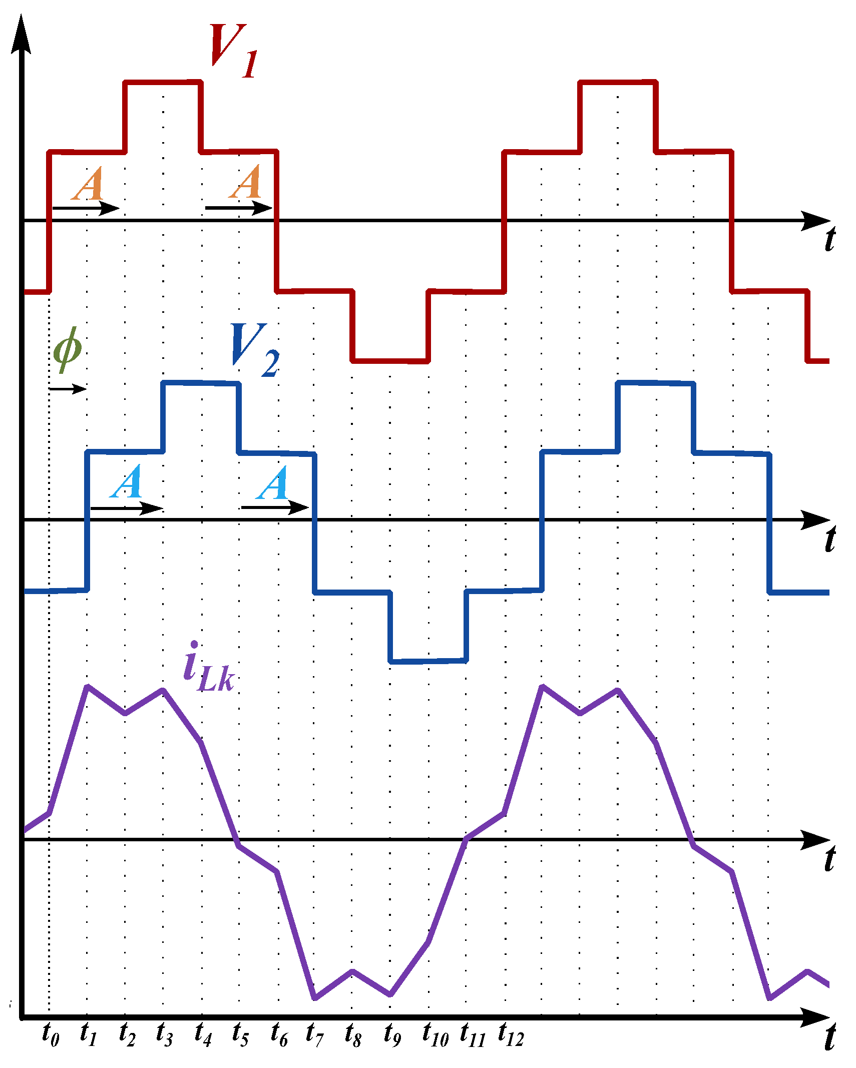
The MAB converter shown in Figure 1 consists of two symmetrical MPC topologies at the input and output. Each one enables the same number of voltage levels and produces similar waveform shapes on its respective sides. These configurations provide diverse injection of power from different inputs. The high-frequency transformer (HFT) has turn ratio N = N S / N P , magnetizing inductance L m , and leakage inductance L k . In steady-state operation, the MAB-based converter can be modeled as two high-frequency AC sources connected across an inductor, where L k represents the sum of the series and leakage inductances of the transformer, V 1 and V 2 are the HFL voltages of the bridges, and i L k is the corresponding HFL current. Figure 2 shows the key operating parameters, with V 1 and V 2 representing the transformer’s input and output voltages and i L k denoting the leakage inductance current. The phase shift ϕ controls energy transfer by defining the angular displacement between the waveforms. The modulation index A determines the fraction of the switching cycle in which power transfer occurs and is the same for both V 1 and V 2 in the given switching pattern. The converter’s various operating states are identified based on its switching pattern. These states are classified using two key parameters: the phase shift between V 1 and V 2 , which is ϕ , and the modulation index A.

3. High-Frequency Link Characterization

3.1. Voltage and Current Characterization

The HFL voltages shown in Figure 2 can be expressed using the Fourier series representation. For the proposed MAB converter, the primary and secondary voltages can be formulated as follows:
V 1 t = n = 1 , n o d d 4 V i n 1 π n + V i n 2 π n M sin n ω 0 t
where n represents the number of odd harmonics. Similarly, the output voltage at the secondary side follows
V 2 t = n = 1 , n o d d 4 V o u t 1 π n + V o u t 2 π n M sin n ω 0 t Φ
The modulation-related term M is
M = cos 2 π n A T s 1 cos π n 2 A T s 1 + cos 2 π A n T s cos π n 2 A + T s T s
and defines the harmonic distribution in V 1 and V 2 , shaping its spectral content based on the modulation strategy.
The HFL in the multilevel topology can be represented by two AC voltage waveforms across an inductor. The current equation can be derived as
i t i 0 = 1 L 0 t V 1 t V 2 t d t .
Because of the symmetry of the switching cycle, the average inductor current is zero over one switching period; hence, in steady-state conditions the current satisfies
i 0 = i T s 2
where T s represents the switching period, and the angular frequency is given by ω 0 = 2 π f s . The inductor current i L k t can be expressed as a Fourier series:
i L k t = 1 L n = 1 , n o d d 4 V i n 1 π n 2 ω 0 + V i n 2 π n 2 ω 0 M cos n ω 0 t + 1 L n = 1 , n o d d 4 V o u t 1 π n 2 N ω 0 + V o u t 2 π n 2 N ω 0 M cos n ω 0 t Φ
The root mean square (RMS) for input voltage of transformer can be derived as follows:
V 1 , R M S = 1 2 n = 1 , n o d d 4 V i n 1 π n + V i n 2 π n M 2
The RMS value of the leakage inductance current is obtained as
i L k , R M S = 1 L π ω 0 . n = 1 , n o d d 1 2 n 4 B n 2 + C n 2 N 2 2 cos ( n Φ ) B n C n N
where
B n = 4 V i n 1 + V i n 2 M C n = 4 V o u t 1 + V o u t 2 M
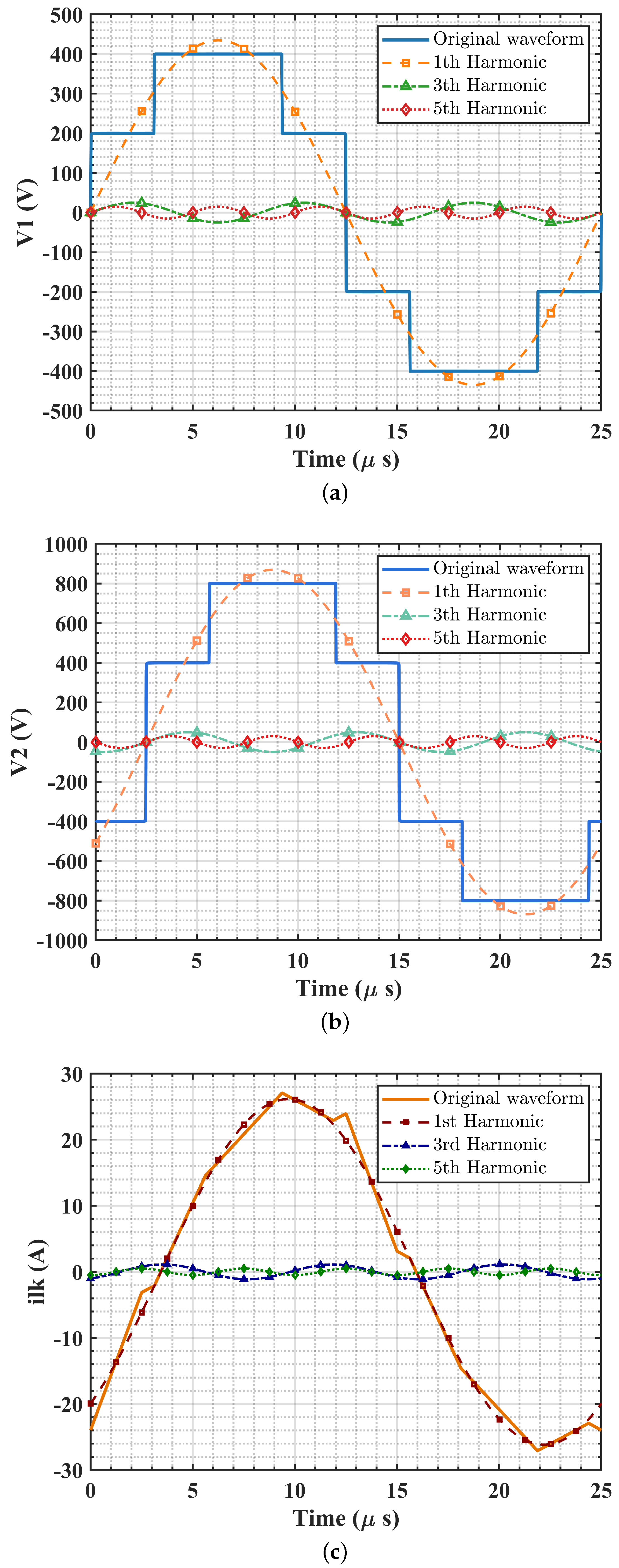
Based on the previous analysis, Figure 3 shows the curves of HFL electrical components for a given modulation index A. The results show that the HFL voltages V 1 and V 2 , together with the leakage inductance current i L k , consist of odd-frequency components only, with overall waveforms consistent with those derived from the conventional piecewise linear method [9].

3.2. Active Power Characterization

The average power transferred in the MAB converter over a single switching period can be expressed as follows:
P = 1 T 0 T V 1 t i L k t d t
Considering (1), (6), and (10), the active power can be expressed as
P = 1 2 L k n = 1 , n o d d 4 V i n 1 π n + V i n 2 π n M . 4 V o u t 1 π n 2 N ω 0 + V o u t 2 π n 2 N ω 0 M sin n Φ .
where N is the turn ratio of transformer.
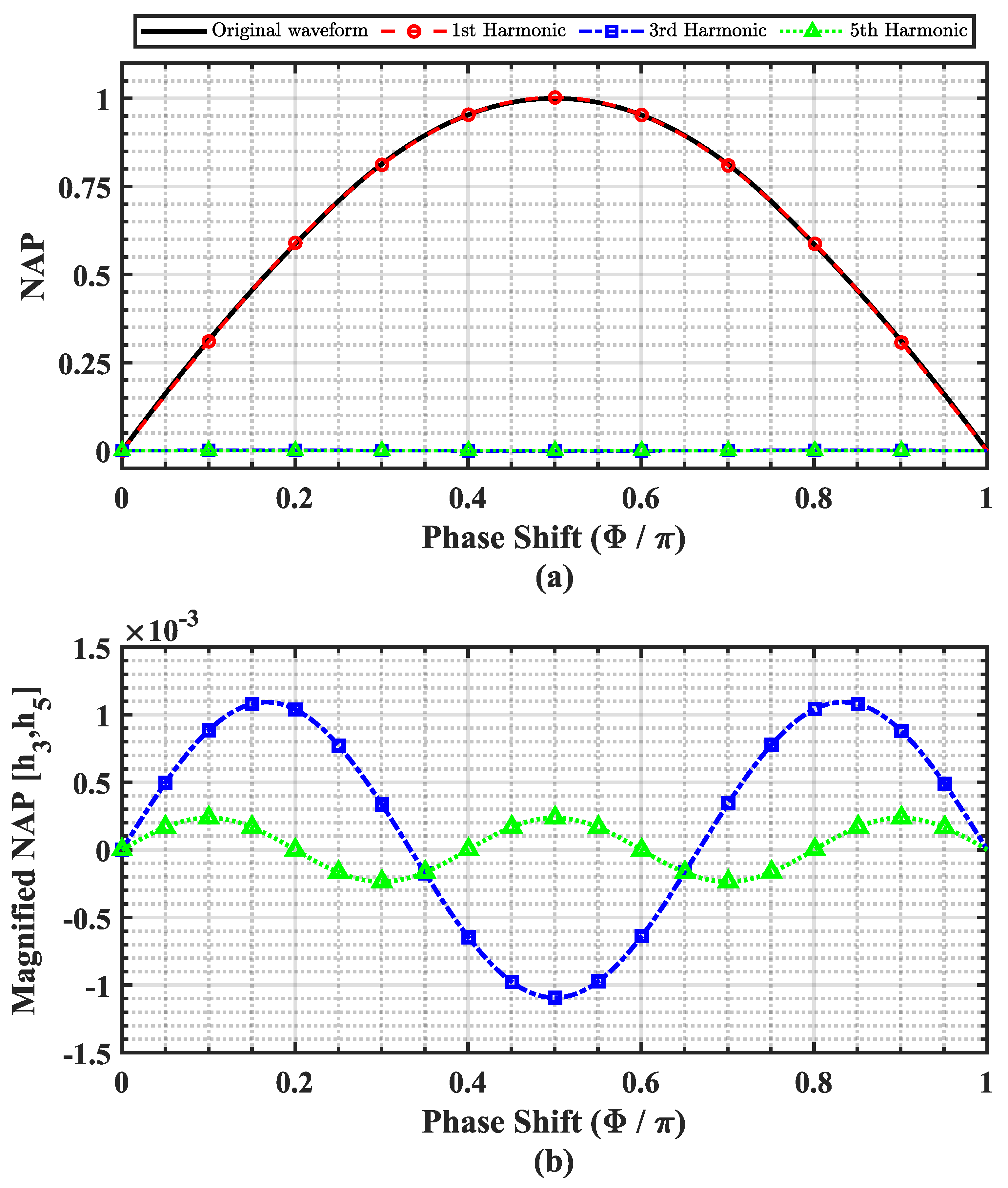
If the active power corresponding to the HFL voltage and current at the same frequency in (1) and (6) is defined in (11), the total power of the MAB-based converter is obtained as the sum of their respective mean components. The active power is primarily influenced by the odd-frequency components and has a symmetry around the mean axis at π / 2 . In Figure 4a, all power components are normalized as normalized active power (NAP), followed by the conventional piecewise linear model.
Of all the harmonics, the fundamental component of the HFL electrical quantities has the largest amplitude, with its power component closely matching the total active power. However, the third harmonic introduces a destructive effect that reduces the overall power, particularly in conventional TAB converters that are more prone to high third-harmonic content. Figure 4b also provides an enlarged view of the third and fifth harmonics to illustrate their impact on system performance.

4. Analysis of HFL Circulating Current

4.1. HFL Reactive Power in MAB Converter

In conventional QAB, the primary function is active power transfer. However, the presence of AC HFL introduces reactive power interactions among the HFL electrical quantities, increasing apparent power and RMS current. This leads to higher power dissipation, greater capacity requirements, and large circulating currents, reducing system efficiency. In addition, the third-harmonic components in the active power are more pronounced in conventional QAB, further increasing the reactive power. This problem can be mitigated in the MAB converter by applying a modulation index A. The total reactive power Q is given by
Q = S 2 P 2
where the apparent power S is
S = V 1 , R M S . i L k , R M S

4.2. Circulating Current and HFL Power Factor

Reactive power interactions have a significant influence on the circulating current behavior. The HFL power factor (HFL-PF) effectively characterizes these interactions and is defined as
φ = P S
Using (11), (13), and (14), the power factor can be written as follows:
φ = π ω 0 2 . n = 1 , n o d d X n Y n sin n Φ 1 2 n = 1 , n o d d X n 2 · n = 1 , n o d d 1 2 n 4 Y n 2 2 cos n Φ X n Y n
X n = 4 V i n 1 π n + V i n 2 π n M Y n = 4 V o u t 1 π n 2 N ω 0 + V o u t 2 π n 2 N ω 0 M
where the terms X n and Y n denote the input- and output-voltage-dependent expressions, respectively.
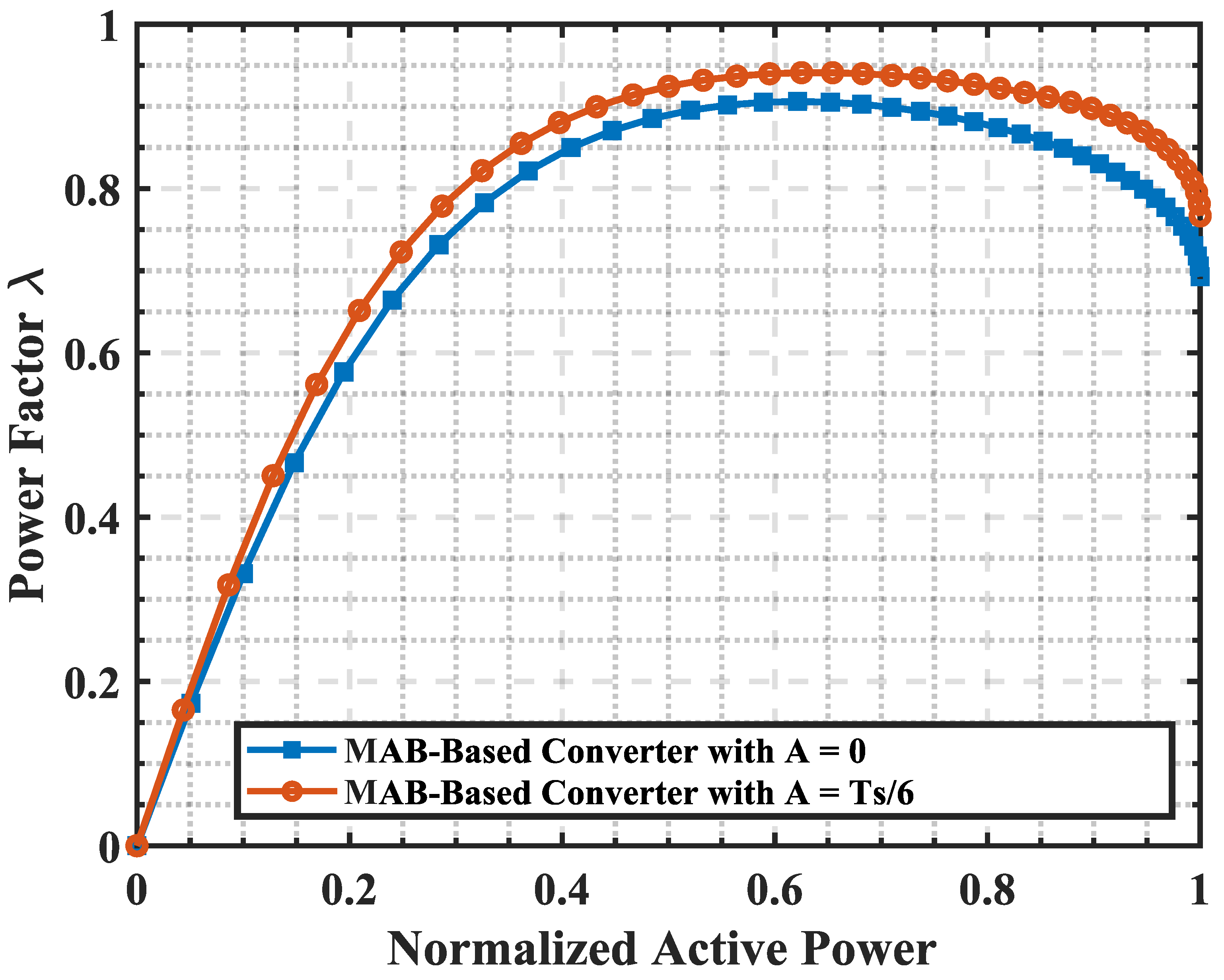
According to (15), Figure 5 compares the variation in HFL-PF and active power between the proposed MAB A = T s / 6 and the conventional QAB (same as MAB converter with A = 0 ). The results show that the HFL-PF initially increases with the phase shift and then decreases, reaching a maximum at a certain point. This trend highlights the advantages of modulation-based optimization in improving power transfer efficiency.

5. Power Loss Modeling and Optimization

5.1. Theoretical Basis for Power Loss

The accurate modeling of power losses is crucial for selecting appropriately rated semiconductor switches, ensuring reliable operation, and minimizing total system losses. In this work, C3M0030090K switches [24] are used on the input side, while C3M0065090D [25] switches are used on the output side.
The conduction and switching parameters of these MOSFETs, obtained from data sheets and simulation conditions, are as follows: on-state resistance R D S ( O N ) = 65 m Ω (C3M0030090K) and 90 m Ω (C3M0065090D), rise time t r = 20 ns, fall time t f = 25 ns, switching frequency f s w = 40 kHz, and peak current I p e a k 20 A . These values were used in calculating both conduction losses (27) and switching losses (28). Including these parameters ensures completeness and reproducibility of the loss modeling.
In an isolated multilevel DC–DC converter, such as the proposed MAB, power losses mainly result from the interaction between high-frequency voltages and the circulating current across the transformer’s leakage inductance. These losses, often underestimated in simplified models, significantly affect the converter’s efficiency and power factor, especially under varying modulation and phase-shift conditions.

5.2. RMS Current Derivations

5.2.1. Switching Patterns

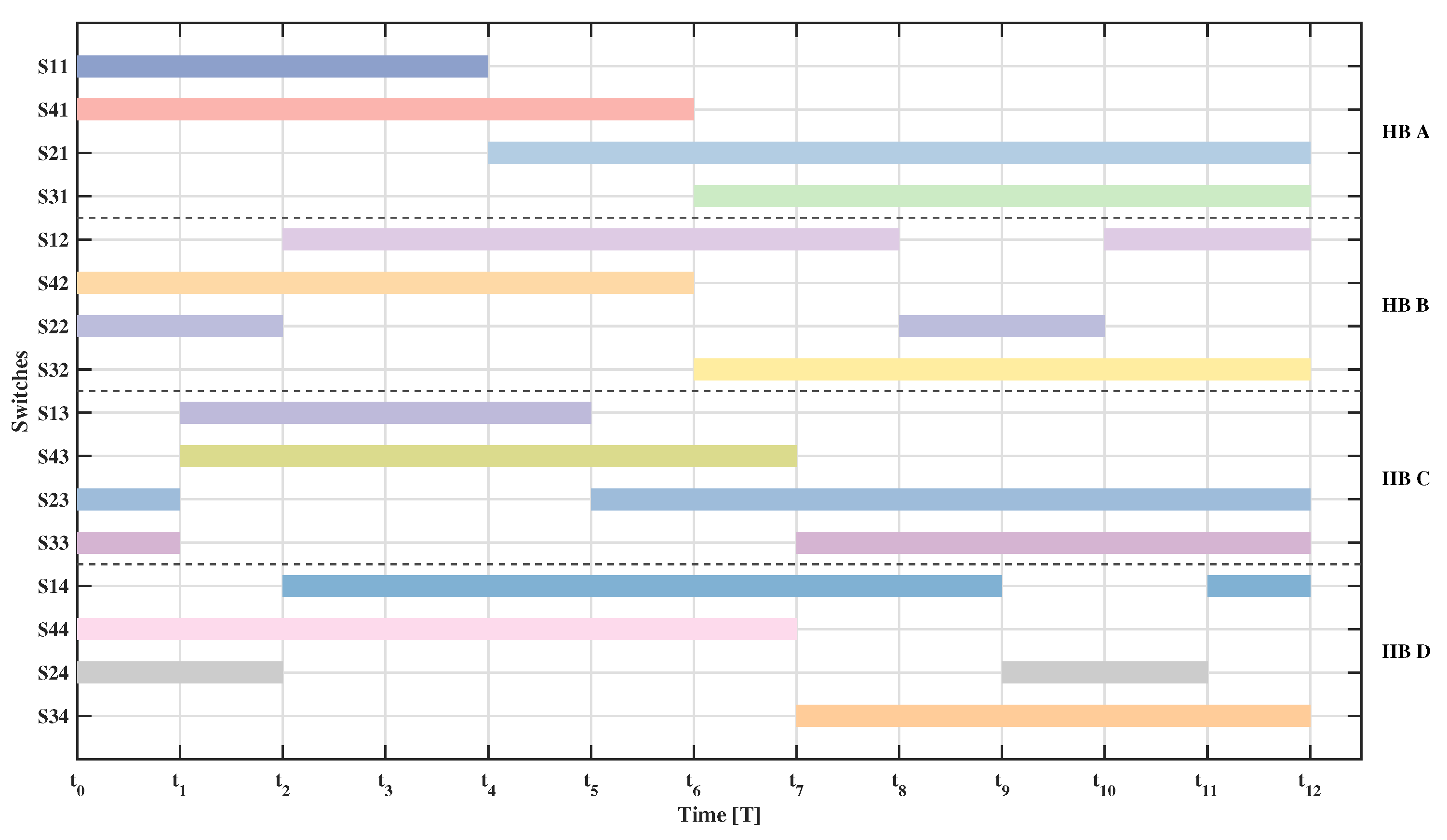
The MAB uses 16 switching signals for the 16 power switches, as shown in Figure 6. Each switch operates at specific instants in a sequence labeled from t 0 to t 12 . Using the waveform diagram in Figure 6, the instantaneous current for each switch is derived. The following equations demonstrate current profiles using a piecewise linear ramp approximation. From Figure 6, the instantaneous values of the currents of all switches are derived here.
The method for calculating the instantaneous currents is given below. Table 1 computes the instantaneous current in a switch during a specific operating interval using a piecewise linear current ramp approach [26]. The eight left-hand side equations are for the input side of the MAB, while the opposite equations in the third column in Table 1 are for the output side of the proposed converter topology. The currents are described as time-dependent piecewise functions over a complete switching cycle, with each interval t i t < t i + 1 representing a distinct switching state governed by the control sequence. Device-level stress, conduction time, and power path evolution over the course of the operation cycle can all be clearly identified with the use of conditional expressions, which also make it possible to determine the current’s direction, polarity, and magnitude for each switching interval. In order to maximize converter efficiency and dependability, this thorough tabulation supports accurate loss modeling, thermal analysis, and switching transition identification.
The equations for the other switches are calculated in the same way using conditional function.
Figure 6 shows the pattern of the “on” switches during each time interval. The instantaneous current in each switch can be modeled by piecewise linear functions across switching segments:
i S x ( t ) = 1 L k j = t u r n - o n - m o d e s V s ( t t j ) , for t [ t j , t j + 1 ]
The generalized equation for the switches’ current used at the input side of H bridge is
i S x i n p u t t = 1 L k B · I ˙ S x t + j V s · t t j
where B is a constant value representing number of operation modes in which the switch is turned on, V s are input and output voltages ( V i n 1 , V i n 2 , V o u t 1 , V o u t 2 ), j is the number of turn-on modes, and t j are corresponding time points for each operation mode. Generalized equation for switches in the H bridge of output side is
i S x o u t p u t t = 1 N 2 L k B · I ˙ S x t + j V s · t t j

5.2.2. Generalized RMS Current Formulas

Here, the derivation of general expressions for calculating the RMS current for switches on both the input and output sides of the full bridges is discussed: the generalized RMS current formula for input side full-bridges and its associated parameter definitions are defined here. Using these expressions, the generalized RMS current for any switch I S x , RMS becomes
I S x , RMS = 1 T 0 T i S x t 2 d t
Further, Equation (20) is expanded as
I S x , RMS ( I n p u t ) = 1 L k T j V j 2 · Δ t j 3 3 + V j · I ˙ S x · Δ t j 2 + I ˙ S x 2 · Δ t j
where V j is the net voltage during the interval j, T is the switching cycle, and I S x , RMS denotes the RMS current through switch x, where x identifies a specific switch within the converter, and L k is the leakage inductance associated with the corresponding leg.
The generalized RMS current formula for output-side full bridges and its associated parameter definitions are defined below in Equation (22) as
I S x , RMS ( o u t p u t ) = 1 N I S x , RMS ( i n p u t ) .
It is important to note that Equations (21) and (22) represent the same RMS current expression applied to different sides of the transformer. Equation (21) corresponds to the input side, where the RMS value is obtained directly from the leakage current waveform. Equation (22) applies the same formulation to the output side but explicitly accounts for the current scaling introduced by the transformer turns ratio N . Since RMS current scales linearly with 1 / N , Equation (22) includes this factor to ensure consistency between input and output representations. This clarification highlights that both equations describe the same physical relationship viewed from opposite sides of the transformer.
To verify the closed-form expressions, RMS currents predicted by the HFL model using the switching-interval relations and (24) were compared with RMS values measured from experimental waveforms under the same operating point used for the loss summary. Using these RMS and peak currents in Equations (27) and (28) yields conduction and switching losses that are consistent with the simulated loss distribution. Small deviations are expected due to device capacitances, dead time, and parasitics not included in the simplified analytical model, and they do not affect the observed trends or conclusions.

5.2.3. Body Diode RMS Currents

Each leg of the full-bridge includes a MOSFET and its intrinsic body diode. Since the diode and switch conduct in alternating half cycles, their RMS currents are approximately equal:
I Dx , RMS I Sx , RMS
This assumption holds unless diode conduction is constrained by specific timing conditions.

5.2.4. Leakage Inductance Current I L k , RMS

This is the key HFL current through the transformer.
i L k , R M S = 1 L π ω 0 . n = 1 , n o d d 1 2 n 4 B n 2 + C n 2 N 2 2 cos ( n Φ ) B n C n N
This RMS current affects all switches symmetrically due to the bidirectional HFL. By utilizing the calculated RMS currents equations, we were able to estimate the conduction and switching losses for each of the full bridges, as seen in Table 1; the loss components were calculated by standard MOSFET models of temperature-independent parameters.

5.3. Parameters Related to Conduction and Switching Losses of the Devices

For the loss evaluation, the electrical characteristics of the switching devices and the physical properties of the transformer that were used in the analysis are listed in Table 2 and Table 3. These values, taken from data sheets and verified where possible with measurements, provide the reference data for the conduction, switching, and transformer loss calculations that follow.

5.4. Transformer Loss Calculations

In addition to the conduction and switching losses of the semiconductor devices, the transformer itself also contributes to the overall loss when circulating current is present. This loss has two main parts: copper loss in the windings and core loss in the magnetic material. The copper loss is proportional to the square of the RMS current in the input and output windings, while the core loss depends on the magnetic flux swing and the operating frequency. Using the RMS link current values obtained from the earlier analysis together with the transformer resistance and core data, the combined copper and core losses were calculated. These transformer losses are included alongside the semiconductor losses in the following Table 4 and Figure 7 to give a complete picture of the loss distribution in the converter.
A high-frequency isolation transformer (E43/28 TP4A ferrite) is used in the experimental setup, designed for 40 kHz operation with turn ratio N = 3 . At Φ = T s 12 , the RMS link current computed is I p , RMS = 9.29 A on the input and I s , RMS = I p , RMS N = 3.10 A on the output. The winding resistances at 40 kHz were obtained from the transformer model at 25 °C, yielding R p = 0.240 Ω and R s = 0.520 Ω . The core loss was taken from the TP4A ferrite model at 40 kHz and the simulated volts per turn. The conduction losses formula for the transformer is given in (25), and the overall transformer losses formula is defined in (26).
P L , Conduction = R p I p , RMS 2 + R s I s , RMS 2
P T L = P L , Core + P L , Conduction

5.5. Semiconductor Losses

The semiconductor losses depend on both conduction and switching losses.

5.5.1. Conduction Losses

Conduction losses occur due to the resistive nature of the switch when it is in the on state. The energy lost during this phase depends on the conduction duration and the RMS current flowing through the device.
P c o n d = I R M S 2 · R ( D S ) o n
R ( D S ) o n : on resistance of the MOSFET.

5.5.2. Switching Losses

They can be considered as the sum of the turn-on and turn-off losses.
P s w = 1 2 V D S I p e a k t r + t f f s w
t r , t f are rise and fall times, and f s w is switching frequency. Table 4 presents the total power loss distribution of semiconductor devices and the efficiency of a high-frequency isolated DC–DC MAB–multilevel converter. It categorizes the types of losses, identifies their exact locations within the converter, and quantifies both the percentage contribution and absolute power loss (in watts) of each component.
The results are summarized in Table 4 and illustrated in Figure 7. The device currents were first obtained from the switching pattern shown in Figure 6 and Table 1. RMS and peak values were then applied in the conduction and switching loss models using data sheet parameters for the Wolfspeed C3M0030090K (input bridges) and C3M0065090D (output bridges). The calculations were performed at the operating point V i n 1 = V i n 2 = 100 V; V o u t 1 = V o u t 2 = 400 V; f s w = 40 kHz; N = 3; L k = 40 μH; A = T s / 6 ; and phase shift Φ = T s 12 . These results were cross-checked against experimental measurements at the same operating point, showing good agreement and confirming the validity of the closed-form loss expressions.
The switching frequency used in this converter is 40 kHz, selected based on a trade-off between switching loss minimization and control response. At this frequency and with relatively fast switching transitions ( t r + t f ) , the total switching losses remain minor compared to conduction losses, as evident from the loss breakdown in Table 4 and Figure 7. This validates the effectiveness of the chosen switching strategy and explains the low switching loss contribution indicated in the analysis. The dominant losses are conduction losses, observed primarily at both the input and output sides, especially in H-bridge A (HB A) and H-bridge B (HB B). Switching losses are comparatively minor. Despite that, the converter achieves an efficiency of 97.61%, indicating an effective design and well-optimized switching strategy.
Furthermore, the chart in Figure 7 complements the data in Table 4 by providing a visual representation of the power loss distribution, enabling easier identification of components with significant losses. This visualization highlights areas where improvements, such as minimizing conduction paths, could lead to further efficiency gains. Simulations were conducted in MATLAB R2024a/PLECS Blockset 4.9.5 using actual switching patterns. Figure 6 displays the donut chart illustrating the power loss breakdown. The highest losses are attributed to conduction losses in input-side HB1 and HB2, followed by moderate losses at the output. Switching losses remain relatively low.
Table 4 and Figure 7 detail the power loss distribution across all switches, with a total loss of 16.69 W. Conduction losses constitute approximately 74%, while switching losses account for the remaining 26%.

6. Simulation Results

The simulation results are analyzed to evaluate the performance of the MAB under different operating conditions. Table 5 presents the key specifications. The effect of phase-shift variations between two cascaded H bridges on the circulating current is investigated, with the modulation index A set to 16.66% of T s for all simulation cases. The corresponding waveforms are shown in Figure 8, Figure 9 and Figure 10.
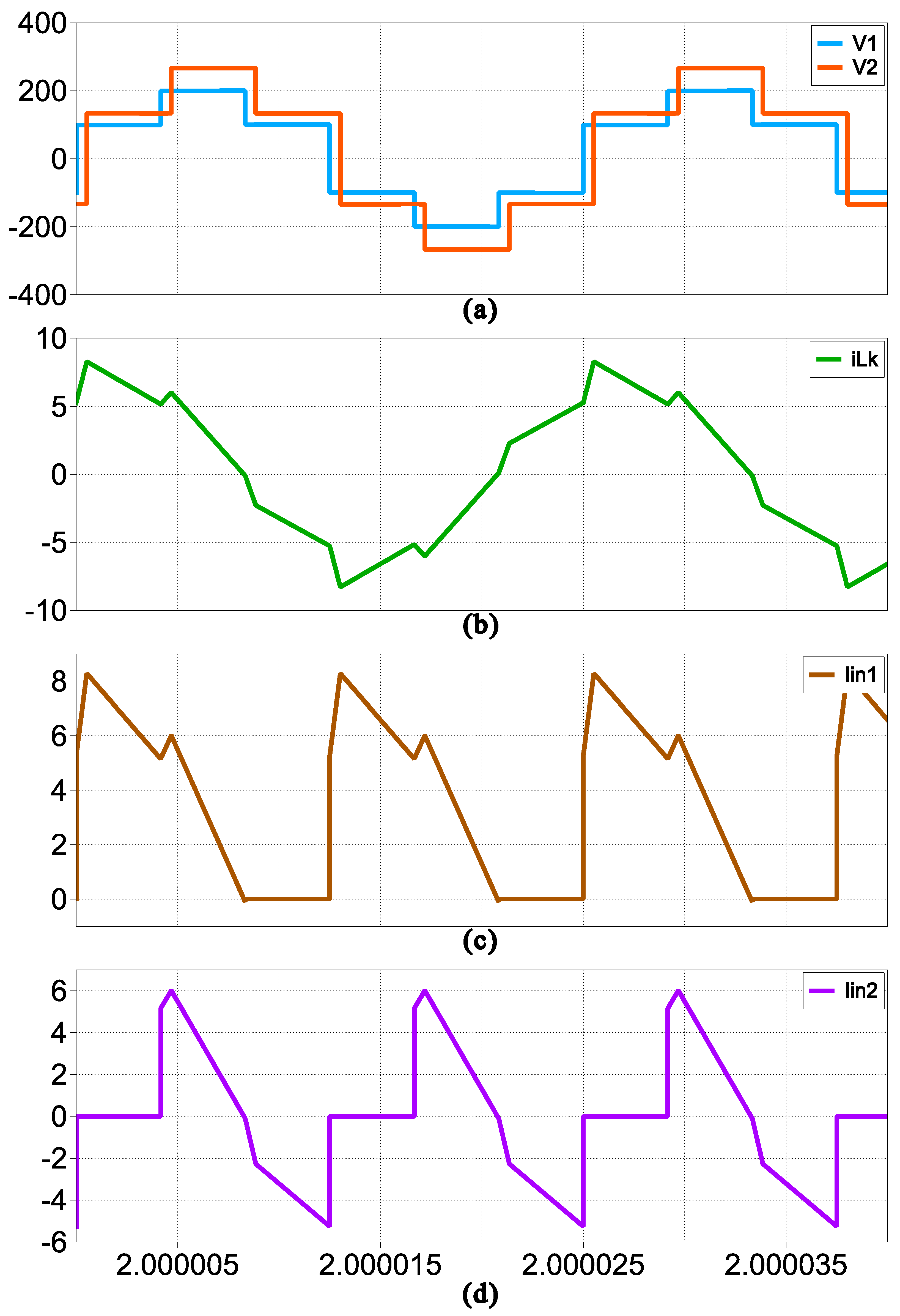
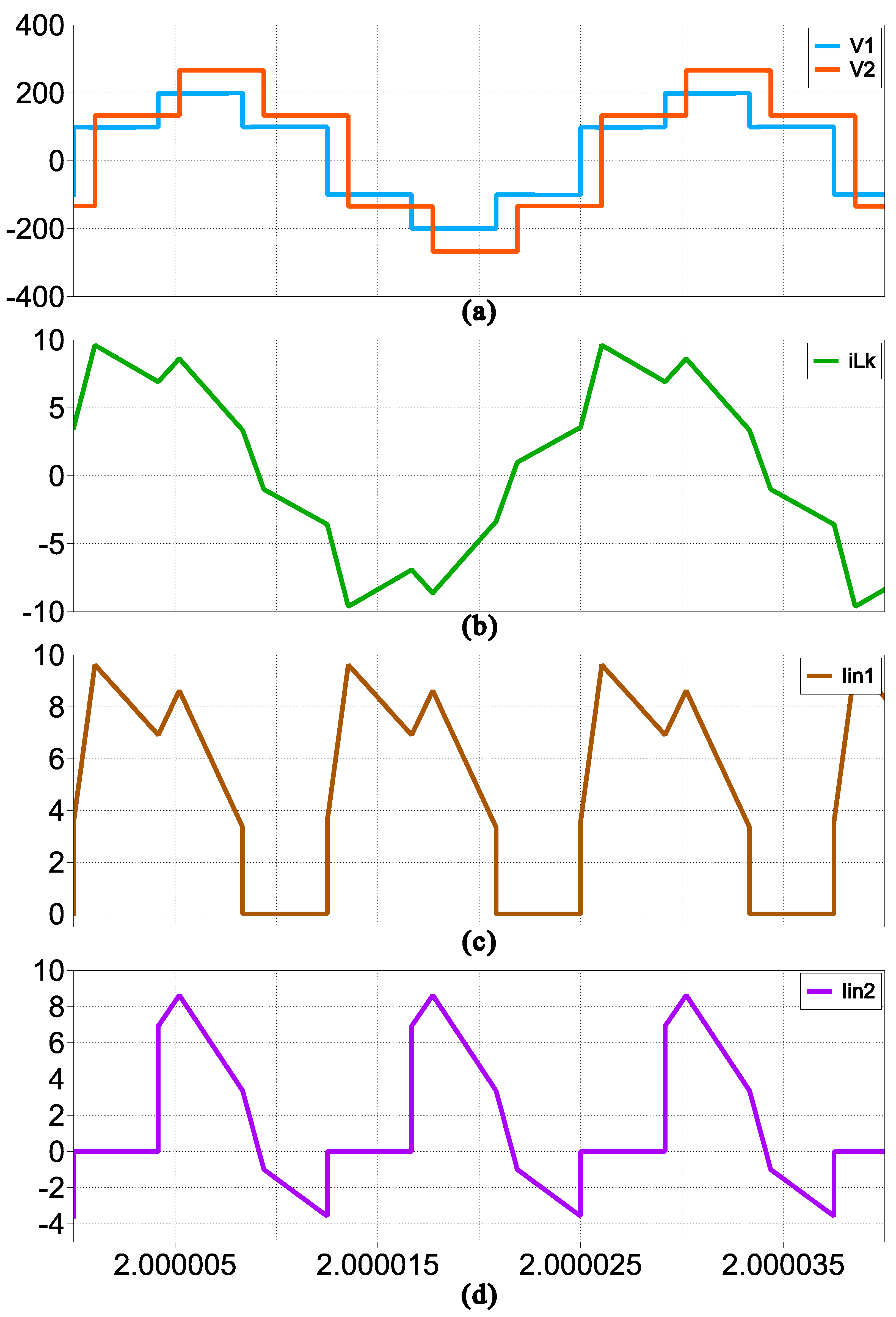
In Figure 8a, the phase shift is defined as T S / 48 . The voltage waveform V 1 , which represents the primary side voltage of the transformer, reaches a maximum of 200 V, as it is the sum of the two input supply voltages. The secondary side voltage V 2 , mirrored onto the input side, reaches a peak value of 266.66 V. The leakage inductance current i L k is also shown in Figure 8b, with an RMS value of 4.95 A. In addition, the input currents I i n 1 and I i n 2 are shown in Figure 8c,d. It is observed that I i n 2 exhibits a significant negative current with a peak amplitude of −5.25 A. This large circulating current at small phase shifts leads to a reduced power factor and consequently lower power transfer efficiency, as reflected in Figure 5. To analyze the system behavior at a higher phase shift, Figure 9 presents the simulation results for Φ = T S / 24 . The voltage waveforms V 1 and V 2 remain unchanged compared to the previous case, as shown in Figure 9a. However, the RMS value of the leakage inductance current i L k increases to 6.11 A, as shown in Figure 9b. The input currents I i n 1 and I i n 2 are also shown in Figure 9c,d. Notably, despite the increase in i L k , the peak negative current in I i n 2 is reduced to −3.57 A. This reduction in negative current indicates an improvement in the power factor, as the extent of circulating power is minimized. Figure 10 shows the simulation results for the phase shift corresponding to the highest power factor efficiency, identified as Φ = T S / 12 . The RMS value of i L k increases further to 9.29 A due to the higher phase shift. As shown in Figure 10b, the mean value of I i n 2 increases compared to the previous cases ( T S / 24 and T S / 48 ). More importantly, the amplitude of the negative current in I i n 2 is significantly reduced to −0.18 A, indicating minimal circulating current. This reduction directly translates into a higher power factor and improved power transfer efficiency in the MAB-based multilevel topology. These results confirm that increasing the phase shift effectively improves the power factor performance by minimizing the circulating currents, leading to improved efficiency in the proposed converter.

7. Experimental Results

In order to evaluate the proposed MAB converter, experimental tests were carried out using a hardware prototype supplied with different voltage levels on the primary and secondary sides of the transformer. The complete system specifications are summarized in Table 6.
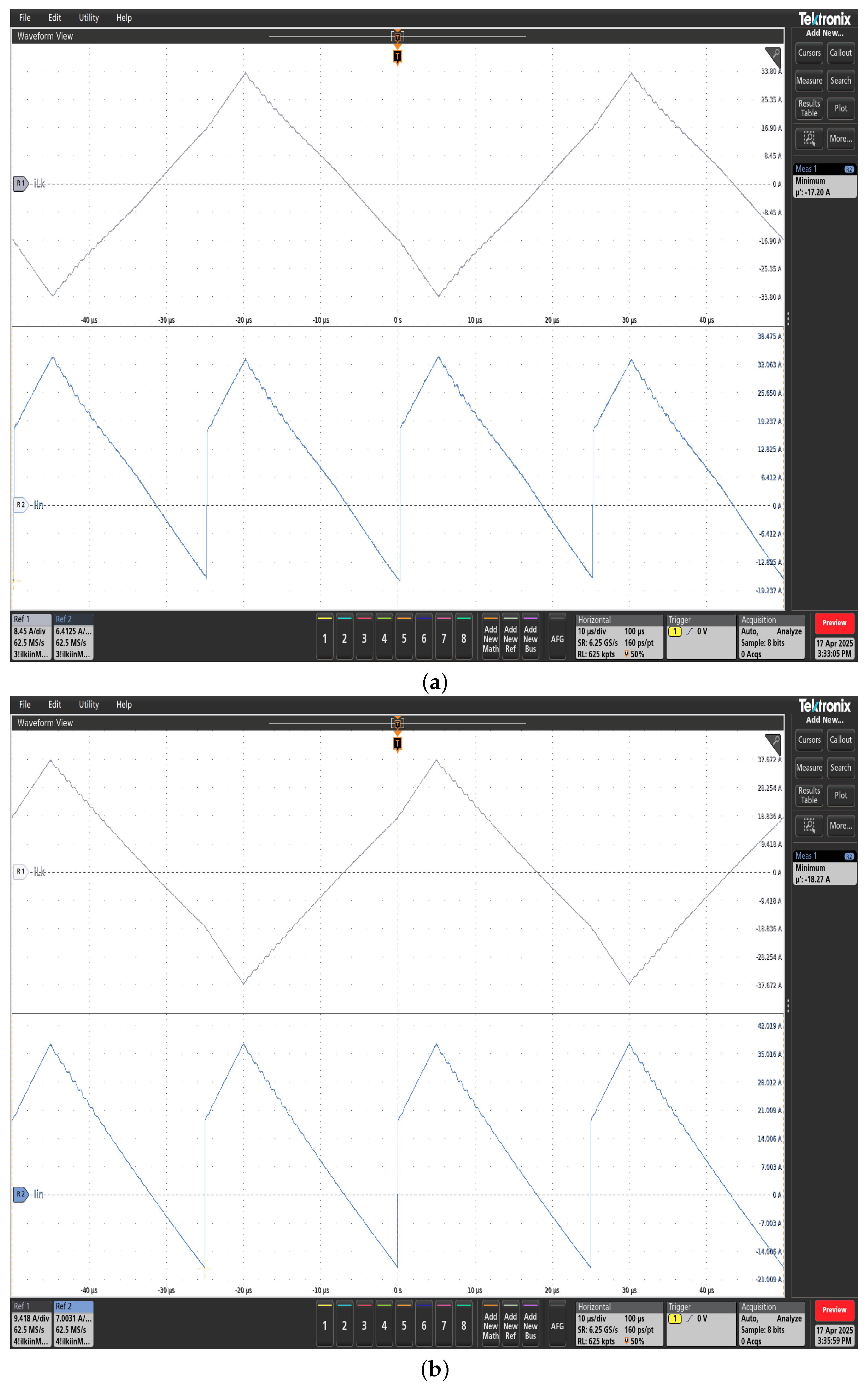
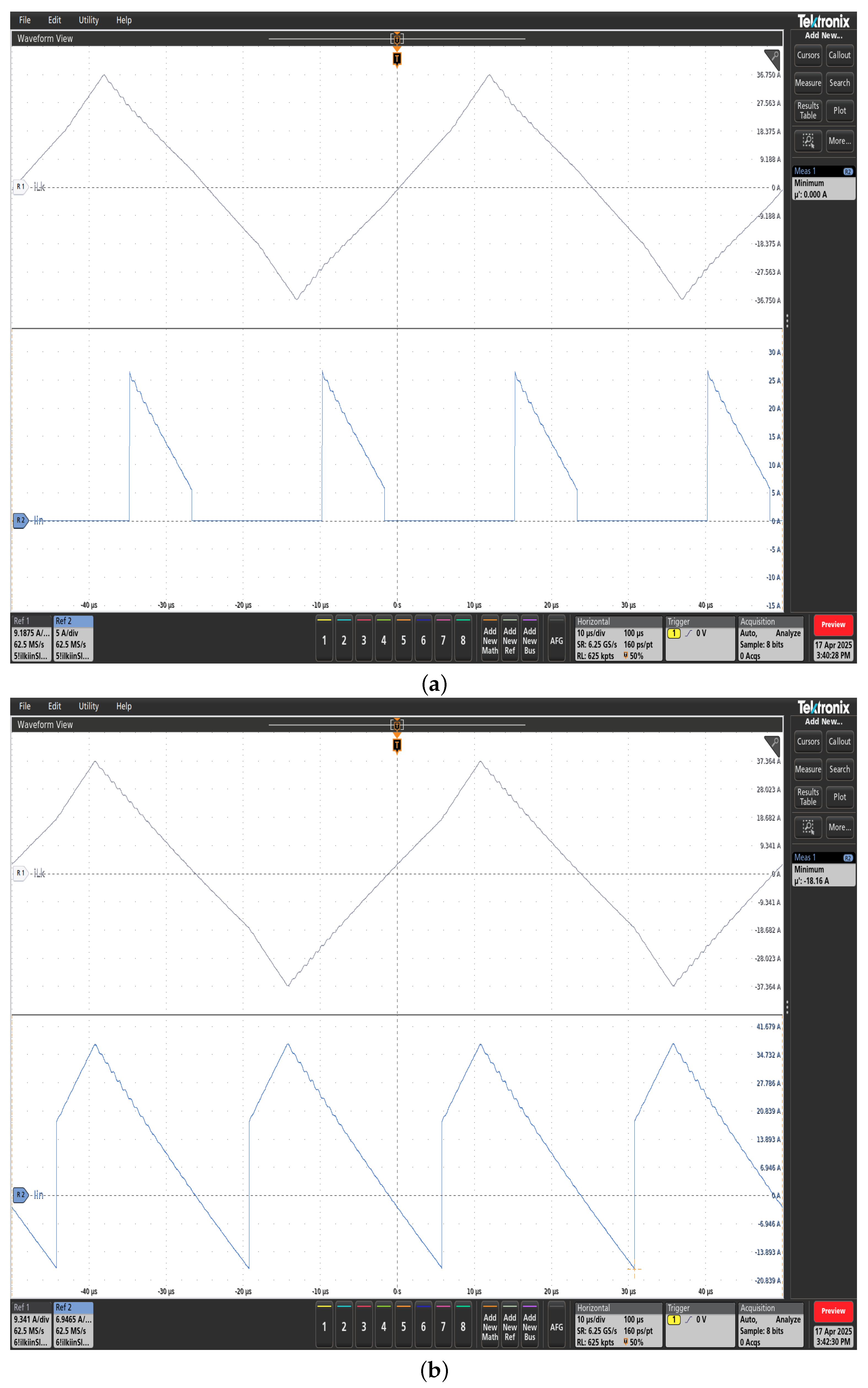
To examine the effect of the MAB-based multilevel converter, the system was tested under two different modulation indices A = 16.66 % and A = 0 % , while maintaining a constant power transfer of 500 W and a fixed phase shift of T S / 12 in both scenarios. Figure 11a,b present the primary and secondary voltage waveforms across the transformer. In Figure 11a, with A = 16.66 % , the primary voltage V 1 of the transformer reaches a peak of 96.97 V, resulting from the combined output of the two H bridges. The secondary voltage V 2 peaks at 376.7 V. When the modulation index is zero [Figure 11b], V 1 drops slightly to 92.66 V, while V 2 increases to 385.7 V. Figure 12a,b show the upper H-bridge current waveforms. With A = 16.66 % , the leakage inductor current exhibits an RMS value of 18.64 A, and the minimum input current is −17.20 A [Figure 12a].
When A = 0 % , these values increase to 20.46 A and −18.27 A [Figure 12b] respectively, indicating that the inclusion of the intermediate voltage level reduces negative current injection by 1.07 A. Figure 13a,b show similar trends for the lower H bridge. In Figure 13a with A = 16.66 % , the minimum input current is fully eliminated, while with A = 0 % , it reaches −18.16 A [Figure 13b]. The RMS values follow the same increase as in the upper H-bridge case. These results confirm that the proposed multilevel modulation strategy significantly reduces the circulating current and minimizes the input current distortion, contributing to improved efficiency and performance of the MAB-based system.
To further validate the effectiveness of the proposed topology, additional measurements were carried out under dynamic load conditions. These tests revealed that the circulating current remained well within the expected theoretical bounds, even when the output load varied from 25% to 100% of rated power. Moreover, the modulation strategy demonstrated high robustness, with minimal impact on output voltage regulation and total harmonic distortion (THD). The observed THD remained below 2% in all scenarios, confirming the quality of the output waveform. These findings strengthen the argument for adopting the MAB-based converter in applications where both efficiency and waveform purity are critical, such as renewable energy interfaces and electric vehicle chargers. In the next section, the results of detailed power loss breakdown and efficiency measurements are presented to further quantify the benefits of the proposed configuration.

8. Conclusions

This paper presents an MAB converter optimized for DC–DC applications that address key challenges such as circulating currents. By exploiting high-frequency link (HFL) analysis, the multilevel converters improve power factor and increase efficiency. Simulation and experimental results confirm that increasing the phase shift minimizes circulating currents, with T S / 12 providing the highest power factor. Compared to conventional QABs, MAB achieves lower transformer weight and superior performance in high-power applications. The inclusion of power loss analysis complements the circulating current and power factor evaluation, offering additional insight into the converter’s practical performance. Experimental tests further validate these findings, showing that the proposed multilevel modulation strategy reduces the reverse input current injection from the converter to the input supplies.

Author Contributions

Conceptualization, M.D.; Methodology, M.D., F.U.R. and A.G.; Software, M.D.; Validation, M.D.; Formal analysis, M.D.; Investigation, M.D.; Resources, M.D.; Data curation, M.D.; Writing—original draft, M.D.; Writing—review & editing, M.D., A.G. and C.C.; Visualization, C.C.; Supervision, A.G. and C.C.; Project administration, C.C.; Funding acquisition, C.C. All authors have read and agreed to the published version of the manuscript.

Funding

This study has been carried out in part within the National Doctorate on Photovoltaics, in part within NEST—Network 4 Energy Sustainable Transition (D.D. 1243 02/08/2022, PE00000021) and has been funded by the National Recovery and Resilience Plan (NRRP), Mission 4, Component 2, Investment 1.3, funded by the European Union—Next GenerationEU and in part within MOST—Sustainable Mobility Centre and was funded by the European Union—Next GenerationEU (PNRR—Mission 4, Component 2, Investment 1.4—D.D. 1033 17/06/2022, CN00000023). The APC is fully waived for this paper. This manuscript expresses the views and opinions of the authors, for which neither the European Union nor the European Commission can be held responsible.

Conflicts of Interest

The authors declare no conflicts of interest.

Abbreviations

The following abbreviations are used in this manuscript:
AModulation index
BTotal number of switch operation modes
DABDual active bridge
fSwitching frequency
HFLHigh-frequency link
HFTHigh-frequency transformer
I p e a k Peak current
I R M S Root mean square current
I ˙ S x Initial current
i L k Leakage inductance current
jNumber of turn-on modes
L k Leakage inductance
L m Magnetizing inductance
MModulation-related term
MABMultiple active bridge
MVMedium voltage
MPCMultiple port converters
NTransformer turn ratio
nNumber of harmonics
NAPNormalized active power
PNominal power
P c o n d Conduction loss
P s w Switching loss
φ Power factor
Φ Phase shift angle
PVPhotovoltaics
QABQuadruple active bridge
QReactive power
R D S ( o n ) On-state resistance of MOSFET
RMSRoot mean square
SApparent power
TABTriple active bridge
T s Switching period
THDTotal harmonic distortion
t r , t f Rise time and fall time of MOSFET
V d s Voltage (drain to source)
V i n 1 , V i n 2 Input voltages
V o u t 1 , V o u t 2 Output voltages
V 1 , V 2 Transformer’s primary and secondary voltages
V s Voltage supplied in the specified interval
ω 0 Angular frequency
xParticular switch within the converter

References

  1. Kumar, L.; Jain, S. Multiple-input DC/DC converter topology for hybrid energy system. IET Power Electron. 2013, 6, 1483–1501. [Google Scholar] [CrossRef]
  2. Dezhbord, M.; Babalou, M.; Mohammadsalehian, S.; Rabiul Islam, M. SIMO DC-DC Converter with a Multi-Winding Coupled Inductor to Reduce Input Current Ripple. In Proceedings of the 2022 IEEE IAS Global Conference on Emerging Technologies (GlobConET), Arad, Romania, 20–22 May 2022; pp. 1043–1048. [Google Scholar] [CrossRef]
  3. Bossi, G.; Buccella, C.; Cecati, C.; Damiano, A.; Floris, A.; Simonetti, F. A Converter Topology for Auxiliary Power System of an All Electric Aircraft. In Proceedings of the 2023 IEEE Energy Conversion Congress and Exposition (ECCE), Nashville, TN, USA, 29 October–2 November 2023; pp. 1605–1612. [Google Scholar] [CrossRef]
  4. Costa, L.F.; Buticchi, G.; Liserre, M. Quadruple Active Bridge DC-DC converter as the basic cell of a modular Smart Transformer. In Proceedings of the 2016 IEEE Applied Power Electronics Conference and Exposition (APEC), Long Beach, CA, USA, 20–24 March 2016; pp. 2449–2456. [Google Scholar] [CrossRef]
  5. Bai, H.; Nie, Z.; Mi, C.C. Experimental Comparison of Traditional Phase-Shift, Dual-Phase-Shift, and Model-Based Control of Isolated Bidirectional DC–DC Converters. IEEE Trans. Power Electron. 2010, 25, 1444–1449. [Google Scholar] [CrossRef]
  6. Dezhbord, M.; Mohamadian, S.; Ghasemian, A.; Buccella, C.; Cecati, C. Enhancing Voltage Gain and Assessing Current THD in Transformer of Photovoltaic Applications through a New Triple Active Bridge Converter. In Proceedings of the 2024 IEEE 33rd International Symposium on Industrial Electronics (ISIE), Quebec City, QC, Canada, 18–21 June 2024; pp. 1–6. [Google Scholar] [CrossRef]
  7. Zhang, Z.; Ouyang, Z.; Thomsen, O.C.; Andersen, M.A.E. Analysis and Design of a Bidirectional Isolated DC–DC Converter for Fuel Cells and Supercapacitors Hybrid System. IEEE Trans. Power Electron. 2012, 27, 848–859. [Google Scholar] [CrossRef]
  8. Beiranvand, H.; Hoffmann, F.; Pascal, Y.; Hahn, F.; Liserre, M. Multiwinding Transformer Leakage Inductance Optimization for Power Flow Decoupling in Multiport DC-DC Converters. In Proceedings of the 2021 IEEE 15th International Conference on Compatibility, Power Electronics and Power Engineering (CPE-POWERENG), Florence, Italy, 14–16 July 2021; pp. 1–8. [Google Scholar] [CrossRef]
  9. Zhao, B.; Song, Q.; Liu, W.; Liu, G.; Zhao, Y. Universal High-Frequency-Link Characterization and Practical Fundamental-Optimal Strategy for Dual-Active-Bridge DC-DC Converter Under PWM Plus Phase-Shift Control. IEEE Trans. Power Electron. 2015, 30, 6488–6494. [Google Scholar] [CrossRef]
  10. Yang, H.; Xu, W.; Wang, H.; Narayanan, M. Investigation of reverse current for crystalline silicon solar cells—New concept for a test standard about the reverse current. In Proceedings of the 2010 35th IEEE Photovoltaic Specialists Conference (PVSC), Honolulu, HI, USA, 20–25 June 2010; pp. 2806–2810. [Google Scholar] [CrossRef]
  11. Jamshed, J.; Mastromauro, R.A. LV DC/MV AC Power Conversion Interface Based on Asymmetrical Multilevel Converters. In Proceedings of the 2025 IEEE 19th International Conference on Compatibility, Power Electronics and Power Engineering (CPE-POWERENG), Lisbon, Portugal, 18–20 June 2025; pp. 1–7. [Google Scholar] [CrossRef]
  12. Jamshed, J.; Mastromauro, R.A. Filter-Less Sub-Multilevel DC/AC Power Converters for MV Connection. In Proceedings of the 2024 IEEE 18th International Conference on Compatibility, Power Electronics and Power Engineering (CPE-POWERENG), Capri, Italy, 19–21 June 2024; pp. 1–7. [Google Scholar] [CrossRef]
  13. Kurm, S.; Agarwal, V. Dual Active Bridge Based Reduced Stage Multiport DC/AC Converter for PV-Battery Systems. IEEE Trans. Ind. Appl. 2022, 58, 2341–2351. [Google Scholar] [CrossRef]
  14. Kolahian, P.; Tarzamni, H.; Nikafrooz, A.; Hamzeh, M. Multi-port DC–DC converter for bipolar medium voltage DC micro-grid applications. IET Power Electron. 2019, 12, 1841–1849. [Google Scholar] [CrossRef]
  15. Mukherjee, S.; Ruiz, J.M.; Barbosa, P. A High Power Density Wide Range DC–DC Converter for Universal Electric Vehicle Charging. IEEE Trans. Power Electron. 2023, 38, 1998–2012. [Google Scholar] [CrossRef]
  16. Bossi, G.; Buccella, C.; Cecati, C.; Simonetti, F.; Damiano, A. A Battery-Based Auxiliary Power System for an All-Electric Aircraft: A Novel Converter Configuration. IEEE Trans. Ind. Appl. 2025, 1–13. [Google Scholar] [CrossRef]
  17. Pamujula, M.; Ohja, A.; Kulkarni, R.; Swarnkar, P. Cascaded ‘H’ Bridge based Multilevel Inverter Topologies: A Review. In Proceedings of the 2020 International Conference for Emerging Technology (INCET), Belgaum, India, 5–7 June 2020; pp. 1–7. [Google Scholar] [CrossRef]
  18. Meng, X.; Duan, Q.; Sha, G.; Zhao, C.; Wang, H.; Wang, X.; Lan, Z. An Efficiency Improvement Strategy for Triple-Active-Bridge-Based DC Energy Routers in DC Microgrids. Electronics 2024, 13, 1172. [Google Scholar] [CrossRef]
  19. Das, D.; Weise, N.; Basu, K.; Baranwal, R.; Mohan, N. A Bidirectional Soft-Switched DAB-Based Single-Stage Three-Phase AC–DC Converter for V2G Application. IEEE Trans. Transp. Electrif. 2019, 5, 186–199. [Google Scholar] [CrossRef]
  20. Costa, L.F.; Buticchi, G.; Liserre, M. Quad-Active-Bridge DC–DC Converter as Cross-Link for Medium-Voltage Modular Inverters. IEEE Trans. Ind. Appl. 2017, 53, 1243–1253. [Google Scholar] [CrossRef]
  21. Han, J.; Li, X.; Sun, Y.; Gong, S.; Huang, S. Quadruple-active-bridge based unified power quality conditioner-L with fault current limiting capability. Electr. Power Syst. Res. 2022, 206, 107780. [Google Scholar] [CrossRef]
  22. Adam, A.H.A.; Chen, J.; Xu, M.; Kamel, S.; Ali, G. Model predictive control for quad active bridge DC-DC converter for more electric aircraft applications. Sci. Rep. 2025, 15, 13653. [Google Scholar] [CrossRef] [PubMed]
  23. Zhang, L.; Tu, C.; Xiao, F.; Liu, B.; Li, P. Method for Classification and Optimization of Modes in Triple-Active-Bridge Converter Based on Waveform Structural Characteristics Analysis. Electronics 2025, 14, 187. [Google Scholar] [CrossRef]
  24. Wolfspeed. C3M0030090K Silicon Carbide Power MOSFET Datasheet. Wolfspeed Technical Datasheet. 2025, pp. 1–10. Available online: https://www.wolfspeed.com/products/power/c3m0030090k/ (accessed on 21 July 2025).
  25. Wolfspeed. C3M0065090D Silicon Carbide Power MOSFET Datasheet. Wolfspeed Technical Datasheet. 2025, pp. 1–10. Available online: https://www.wolfspeed.com/products/power/sic-mosfets/900v-silicon-carbide-mosfets/c3m0065090d/ (accessed on 21 July 2025).
  26. Dezhbord, M.; Mohseni, P.; Hosseini, S.H.; Mirabbasi, D.; Islam, M.R. A High Step-Up Three-Port DC–DC Converter With Reduced Voltage Stress for Hybrid Energy Systems. IEEE J. Emerg. Sel. Top. Ind. Electron. 2022, 3, 998–1009. [Google Scholar] [CrossRef]
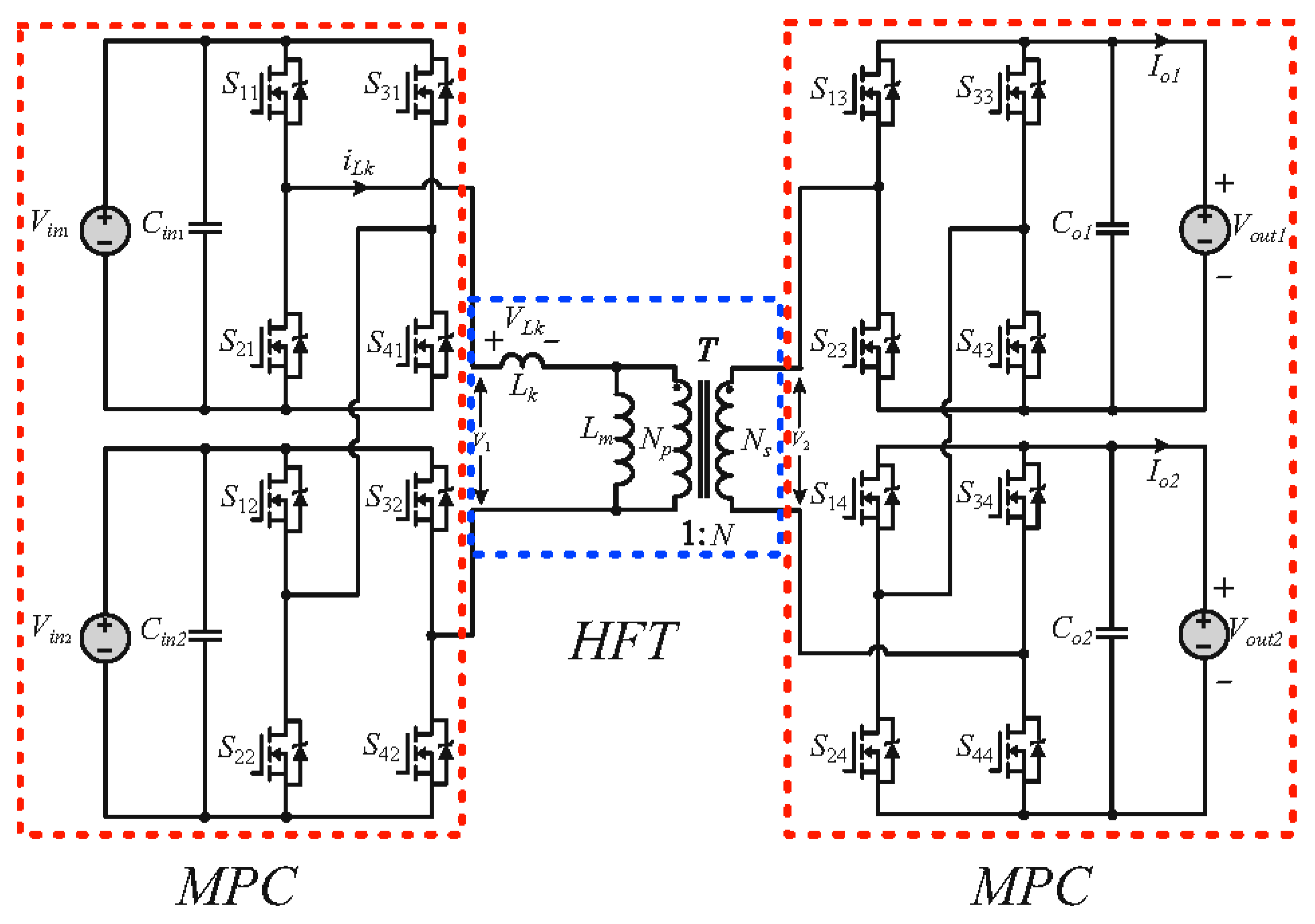
Figure 1. The MAB-based multilevel converter.
Electronics 14 03551 g001
Figure 2. The principle waveforms of the MAB-based multilevel converter.
Electronics 14 03551 g002
Figure 3. Waveform analysis of the HFL electrical components for A = 0.125 T s : (a) HFL voltage V 1 , (b) HFL voltage V 2 , (c) HFL current i L k .
Electronics 14 03551 g003
Figure 4. Normalized active power over one period: (a) NAP variation with phase shift, showing fundamental and harmonic components, (b) magnified view of the 3rd and 5th harmonics.
Electronics 14 03551 g004
Figure 5. Comparison of power factor φ for conventional QAB and MAB converters over normalized active power.
Electronics 14 03551 g005
Figure 6. Switching pattern diagram for the MAB.
Electronics 14 03551 g006
Figure 7. Donut loss distribution chart.
Electronics 14 03551 g007
Figure 8. Simulation results of the MAB converter for the phase shift of T S / 48 : (a) V 1 and V 2 represent primary and secondary voltages, (b) i L k represents leakage inductance current, (c) i i n 1 is the first input current value, (d) i i n 2 is the second input current value.
Electronics 14 03551 g008
Figure 9. Simulation results of the MAB converter for the phase shift of T S / 24 : (a) V 1 and V 2 represent primary and secondary voltages, (b) i L k represents leakage inductance current, (c) i i n 1 is the first input current value, (d) i i n 2 is the second input current value.
Electronics 14 03551 g009
Figure 10. Simulation results of the MAB converter for the phase shift of T S / 12 : (a) V 1 and V 2 represent primary and secondary voltages, (b) i L k represents leakage inductance current, (c) i i n 1 is the first input current value, (d) i i n 2 is the second input current value.
Electronics 14 03551 g010
Figure 11. Primary and secondary voltage waveforms across the transformer with modulation indices A = 16.66% (a) and A = 0% (b).
Electronics 14 03551 g011
Figure 12. Upper H-bridge current waveforms with modulation indices A = 16.66% (a) and A = 0% (b).
Electronics 14 03551 g012
Figure 13. Lower H-bridge current waveforms with modulation indices A = 16.66% (a) and A = 0% (b).
Electronics 14 03551 g013
Table 1. Conditional function expressions for the switches.
SwitchCurrent ExpressionsSwitchCurrent Expressions
i S 11 ( t ) 1 L k V i n 1 , t 0 t < t 1 V i n 1 , t 1 t < t 2 V i n 1 + V i n 2 , t 2 t < t 3 V i n 1 + V i n 2 . t 3 t < t 4 i S 13 ( t ) 1 N 2 L k V i n 1 + V i n 2 , t 1 < t < t 2 V i n 1 + V i n 2 + V o u t 1 , t 2 < t < t 3 V i n 1 + V i n 2 + V o u t 1 + V o u t 2 , t 3 < t < t 4 V i n 1 + V i n 2 + V o u t 1 + V o u t 2 . t 4 < t < t 5
i S 41 ( t ) 1 L k V i n 1 , t 0 < t < t 1 V i n 1 , t 1 < t < t 2 V i n 1 + V i n 2 , t 2 < t < t 3 V i n 1 + V i n 2 , t 3 < t < t 4 V i n 2 , t 4 < t < t 5 V i n 2 . t 5 < t < t 6 i S 43 1 N 2 L k V i n 1 + V o u t 1 , t 1 < t < t 2 V i n 1 + V i n 2 + V o u t 1 , t 2 < t < t 3 V i n 1 + V i n 2 + V o u t 1 + V o u t 2 , t 3 < t < t 4 V i n 2 + V o u t 1 + V o u t 2 , t 4 < t < t 5 V i n 2 + V o u t 2 , t 5 < t < t 6 V i n 1 + V o u t 2 . t 6 < t < t 7
i S 21 ( t ) 1 L k V i n 2 , t 4 < t < t 5 V i n 2 , t 5 < t < t 6 V i n 1 , t 6 < t < t 7 V i n 1 , t 7 < t < t 8 V i n 1 V i n 2 , t 8 < t < t 9 V i n 1 V i n 2 , t 9 < t < t 10 V i n 1 , t 10 < t < t 11 V i n 1 . t 11 < t < t 12 i S 23 ( t ) 1 N 2 L k V i n 1 , t 0 < t < t 1 V i n 2 + V o u t 2 , t 5 < t < t 6 V i n 1 + V o u t 2 , t 6 < t < t 7 V i n 1 V o u t 1 , t 7 < t < t 8 V i n 1 V i n 2 V o u t 1 , t 8 < t < t 9 V i n 1 V i n 2 V o u t 1 V o u t 2 , t 9 < t < t 10 V i n 1 V o u t 1 V o u t 2 , t 10 < t < t 11 V i n 1 V o u t 1 . t 11 < t < t 12
i S 31 ( t ) 1 L k V i n 1 , t 6 < t < t 7 V i n 1 , t 7 < t < t 8 V i n 1 V i n 2 , t 8 < t < t 9 V i n 1 V i n 2 , t 9 < t < t 10 V i n 1 , t 10 < t < t 11 V i n 1 . t 11 < t < t 12 i S 33 ( t ) 1 N 2 L k V i n 1 V o u t 1 , t 0 < t < t 1 V i n 1 V o u t 1 , t 7 < t < t 8 V i n 1 V i n 2 V o u t 1 , t 8 < t < t 9 V i n 1 V i n 2 V o u t 1 V o u t 2 , t 9 < t < t 10 V i n 1 V o u t 1 V o u t 2 , t 10 < t < t 11 V i n 1 V o u t 1 . t 11 < t < t 12
i S 12 ( t ) 1 L k V i n 1 + V i n 2 , t 2 < t < t 3 V i n 1 + V i n 2 , t 3 < t < t 4 V i n 2 , t 4 < t < t 5 V i n 2 , t 5 < t < t 6 V i n 1 , t 6 < t < t 7 V i n 1 , t 7 < t < t 8 V i n 1 , t 10 < t < t 11 V i n 1 . t 11 < t < t 12 i S 14 ( t ) 1 N 2 L k V i n 1 + V i n 2 + V o u t 1 , t 2 < t < t 3 V i n 1 + V i n 2 + V o u t 1 + V o u t 2 , t 3 < t < t 4 V i n 2 + V o u t 1 + V o u t 2 , t 4 < t < t 5 V i n 2 + V o u t 2 , t 5 < t < t 6 V i n 1 + V o u t 2 , t 6 < t < t 7 V i n 1 V o u t 1 , t 7 < t < t 8 V i n 1 V i n 2 V o u t 1 , t 8 < t < t 9 V i n 1 V o u t 1 . t 11 < t < t 12
i S 42 ( t ) 1 L k V i n 1 , t 0 < t < t 1 V i n 1 , t 1 < t < t 2 V i n 1 + V i n 2 , t 2 < t < t 3 V i n 1 + V i n 2 , t 3 < t < t 4 V i n 2 , t 4 < t < t 5 V i n 2 . t 5 < t < t 6 i S 44 ( t ) 1 N 2 L k V i n 1 V o u t 1 , t 0 < t < t 1 V i n 1 V o u t 1 , t 1 < t < t 2 V i n 1 + V i n 2 + V o u t 1 , t 2 < t < t 3 V i n 1 + V i n 2 + V o u t 1 + V o u t 2 , t 3 < t < t 4 V i n 2 + V o u t 1 + V o u t 2 , t 4 < t < t 5 V i n 2 + V o u t 2 , t 5 < t < t 6 V i n 1 + V o u t 2 . t 6 < t < t 7
i S 22 ( t ) 1 L k V i n 1 , t 0 < t < t 1 V i n 1 , t 1 < t < t 2 V i n 1 V i n 2 , t 8 < t < t 9 V i n 1 V i n 2 . t 9 < t < t 10 i S 24 ( t ) 1 N 2 L k V i n 1 V o u t 1 , t 0 < t < t 1 V i n 1 + V o u t 1 , t 1 < t < t 2 V i n 1 V i n 2 V o u t 1 V o u t 2 , t 2 < t < t 10 V i n 1 V o u t 1 V o u t 2 , t 10 < t < t 11
i S 32 ( t ) 1 L k V i n 1 , t 6 < t < t 7 V i n 1 , t 7 < t < t 8 V i n 1 V i n 2 , t 8 < t < t 9 V i n 1 V i n 2 , t 9 < t < t 10 V i n 1 , t 10 < t < t 11 V i n 1 . t 11 < t < t 12 i S 34 ( t ) 1 N 2 L k V i n 1 V o u t 1 , t 7 < t < t 8 V i n 1 V i n 2 V o u t 1 , t 8 < t < t 9 V i n 1 V i n 2 V o u t 1 V o u t 2 , t 9 < t < t 10 V i n 1 V o u t 1 V o u t 2 , t 10 < t < t 11 V i n 1 V o u t 1 , t 11 < t < t 12
Table 2. Parameters of switching elements used in loss modeling.
ParameterSymbolValue and Description
On-state resistance
at 25 °C
R D S ( o n ) , 25C3M0030090K:
30 m Ω typ, 39 m Ω max
at V g s = 15 V, I d = 35 A.
C3M0065090D:
65 m Ω typ, 78 m Ω max
at V g s = 15 V, I d = 20 A.
Temperature coefficient
of R D S ( o n )
-C3M0030090K:
≈1.3× at 100 °C, ≈1.7–1.8×
at 150 °C relative to 25 °C.
C3M0065090D:
≈1.25–1.3× at 100 °C,
≈1.6–1.7× at 150 °C.
Turn-on energy E o n (I,V)C3M0030090K:
133 µJ typ at
V d s = 600 V, I d = 35 A.
C3M0065090D:
250 µJ typ at
V d s = 400 V, I d = 20 A.
Turn-off energy E o f f (I,V)C3M0030090K:
111 µJ typ.
C3M0065090D:
48 µJ typ.
Output capacitance energy E o s s (V)C3M0030090K:
~30 µJ typ
from Eoss curve.
C3M0065090D:
~16 µJ typ
from Eoss curve.
Total gate charge Q g C3M0030090K:
74 nC typ.
C3M0065090D:
33 nC typ.
Forward voltage drop V f C3M0030090K:
≈4.5 V typ.
C3M0065090D:
≈4.4 V typ.
Reverse recovery charge
and energy
Q r r , E r e c C3M0030090K:
Qrr ≈ 536 nC,
trr ≈ 24 ns.
C3M0065090D:
Qrr ≈ 185 nC,
trr ≈ 28 ns.
Table 3. Transformer parameters used in loss analysis.
ParameterSymbolValue and Description
Switching frequency f s w 300 kHz
Saturation flux density B sat [ T ] 0.51 (25 °C), 0.39 (100 °C)
Initial permeability (25 °C) μ i 2400 ± 25%
Core area A e [ m 2 ] 2.29 × 10 4
Winding resistance at 40 kHz R p , AC , R s , AC [ Ω ] 0.240, 0.520
Magnetic path length e [ m ] 6.0 × 10 2
Core volume V core = A e e [ m 3 ] 1.374 × 10 5
Table 4. Power loss distribution.
Power Loss Distribution(Loss/Total Loss)Power Loss
Conduction Losses of the Input Side of HB_A8.69%4.9621 W
Switching Losses of the Input Side of HB_A0.89%0.5089 W
Conduction Losses of the Input Side of HB_B8.62%4.9235 W
Switching Losses of the Input Side of HB_B3.51%2.0036 W
Conduction Losses of the Output Side of HB_A2.23%1.2732 W
Switching Losses of the Output Side of HB_A1.62%0.9230 W
Conduction Losses of the Output Side of HB_B2.20%1.2586 W
Switching Losses of the Output Side of HB_B1.46%0.8326 W
Total Conduction Losses21.74%12.4174 W
Total Switching Losses7.47%4.2683 W
Transformer Loss70.79%40.44 W
Total Loss-57.1257 W
Efficiency-97.61%
Table 5. Specifications of the simulated MAB-based multilevel converter.
ParameterValue
V i n 1 , V i n 2 100 V
V o u t 1 , V o u t 2 400 V
Leakage inductance ( L k ) 40 µ H
Turn ratio of the transformer ( N ) 3
Frequency ( f ) 40 kHz
Modulation index ( A ) T s / 6
Table 6. Specifications of the experimental MAB-based multilevel converter.
ParameterValue
V i n 1 , V i n 2 48 V
V o u t 1 , V o u t 2 400 V
Leakage inductance ( L k ) 40 µ H
Turn ratio of the transformer ( N ) 2
Frequency ( f ) 20 kHz
Disclaimer/Publisher’s Note: The statements, opinions and data contained in all publications are solely those of the individual author(s) and contributor(s) and not of MDPI and/or the editor(s). MDPI and/or the editor(s) disclaim responsibility for any injury to people or property resulting from any ideas, methods, instructions or products referred to in the content.