
Buck Converter with Improved Efficiency and Wide Load Range Enabled by Negative Level Shifter and Low-Power Adaptive On-Time Controller


Abstract
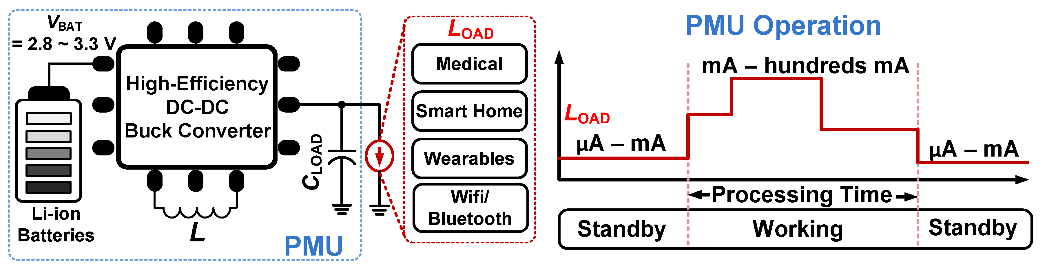
1. Introduction
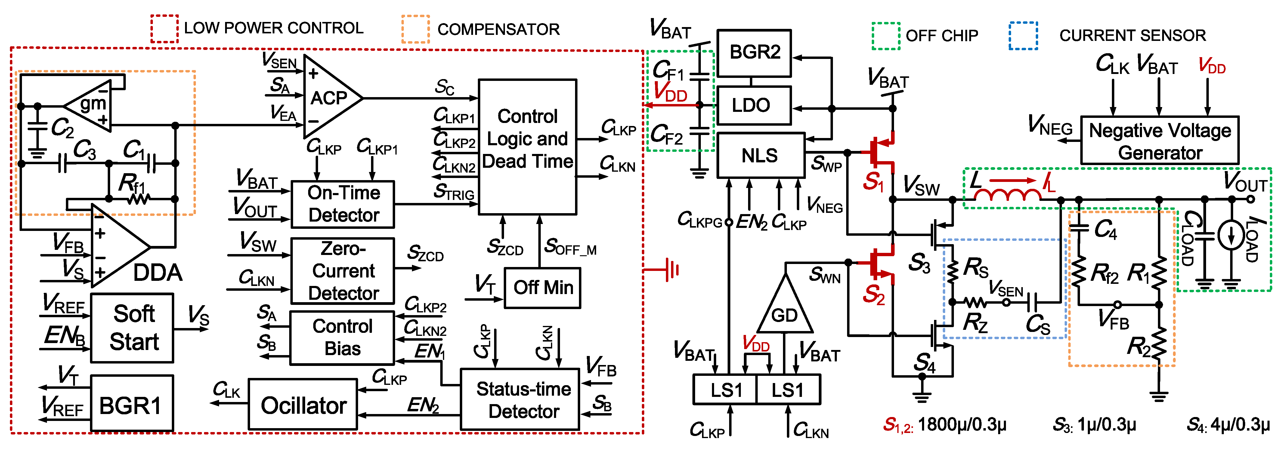
2. The AOT Control Buck Converter Architecture and Circuit Implementations
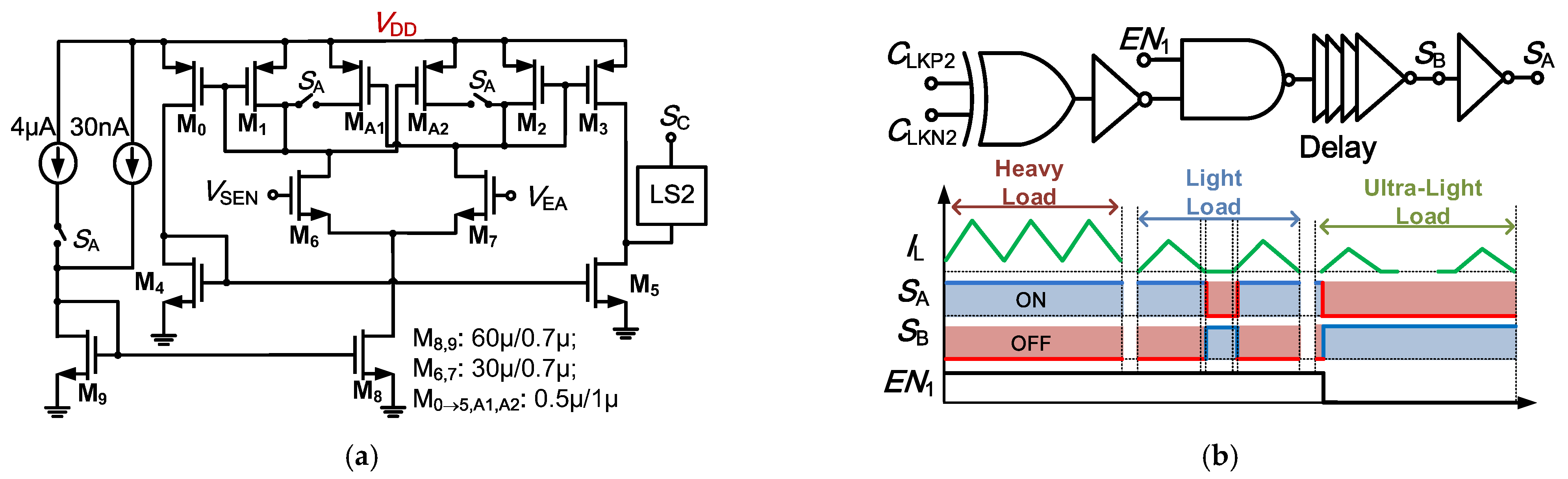
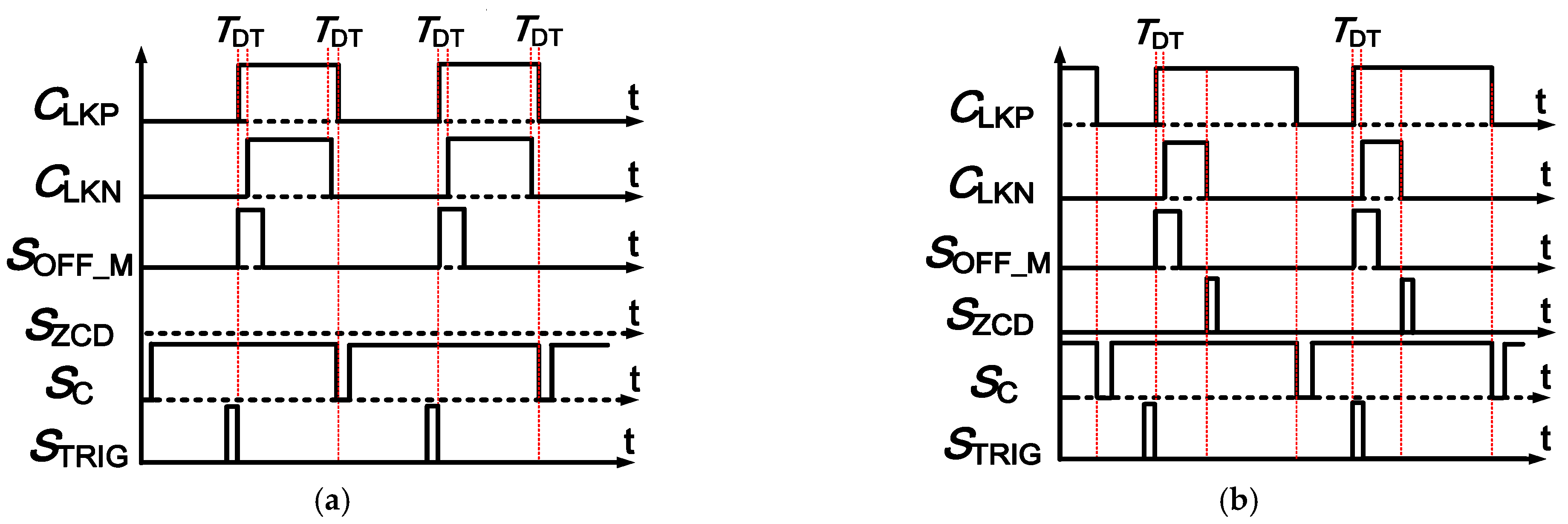
2.1. The Operating Mechanism of the Architecture
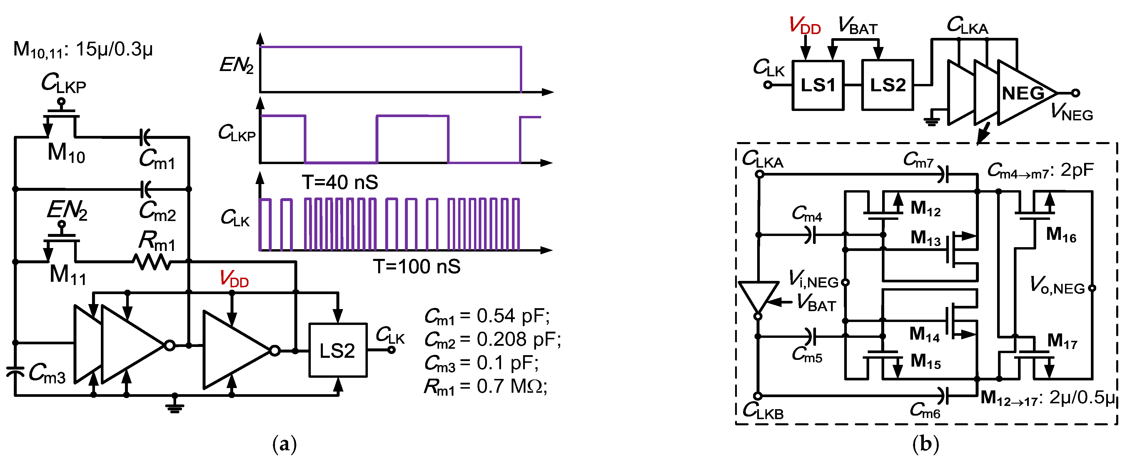
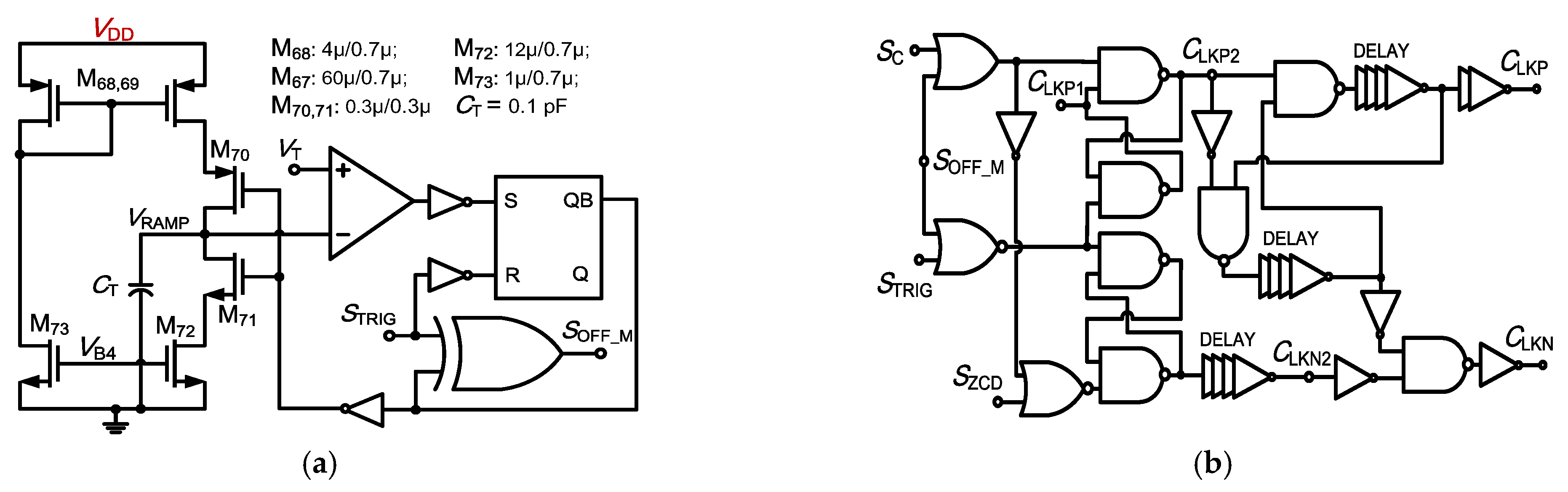
2.2. The Circuit Implementation
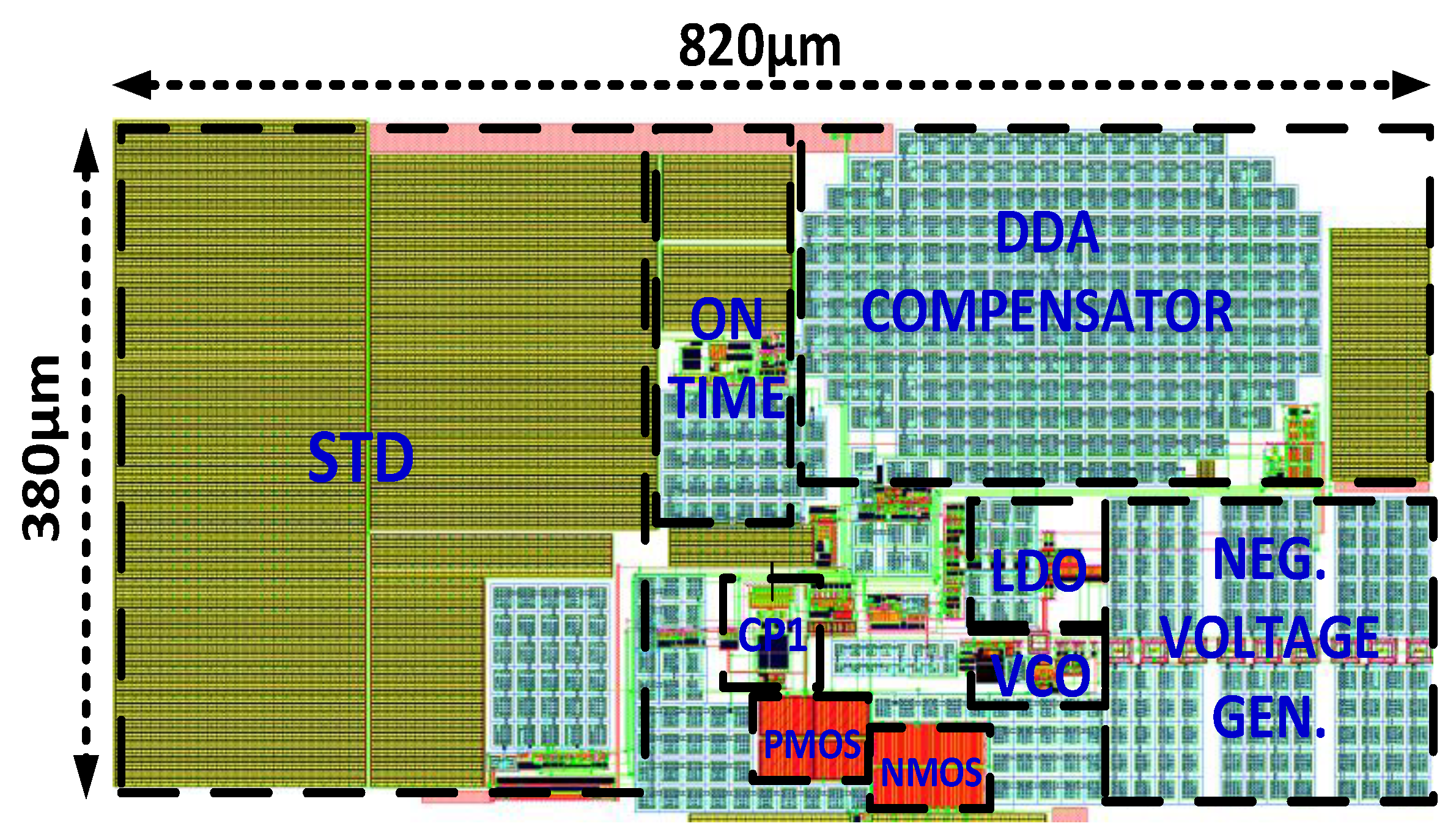
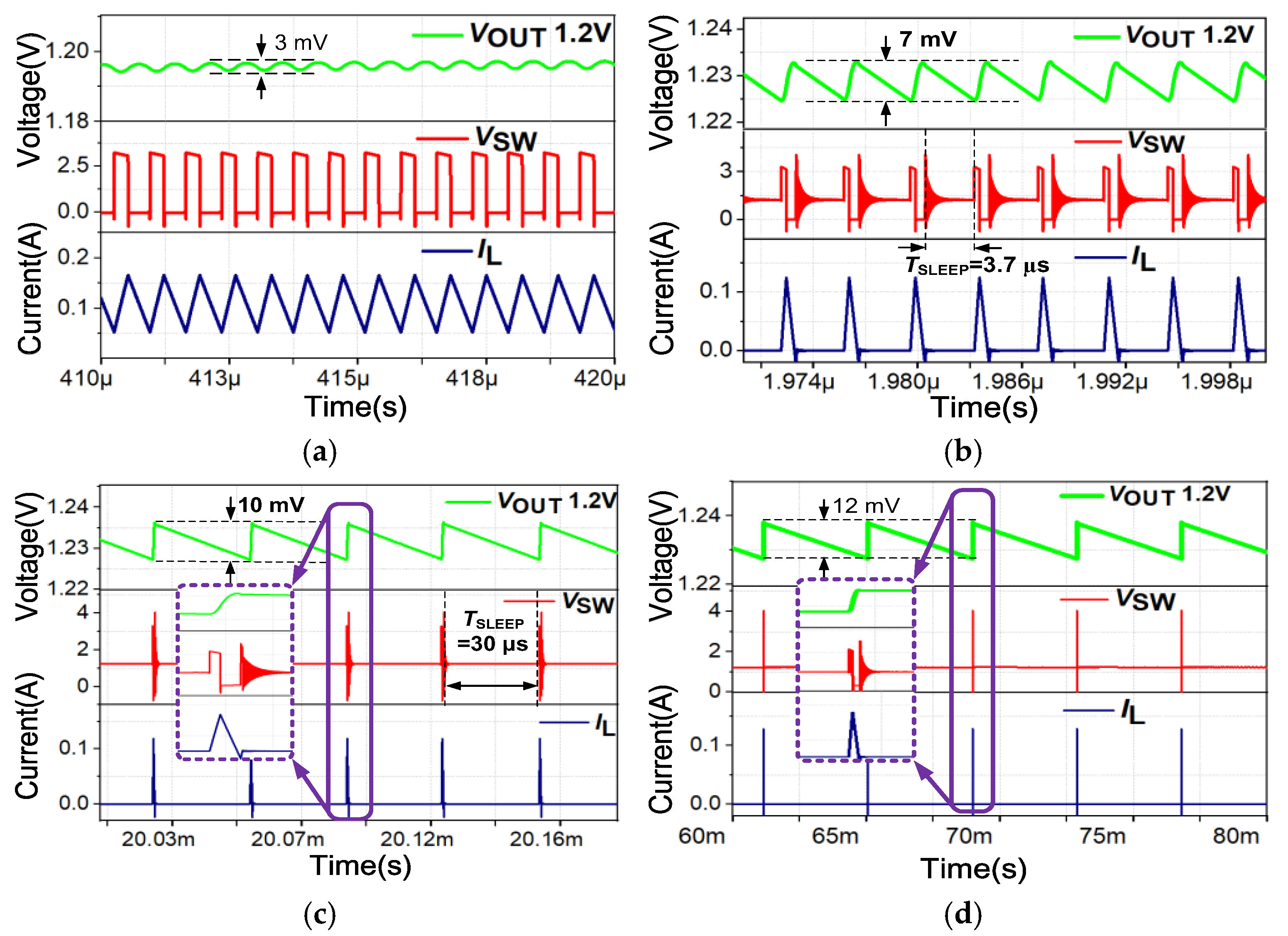
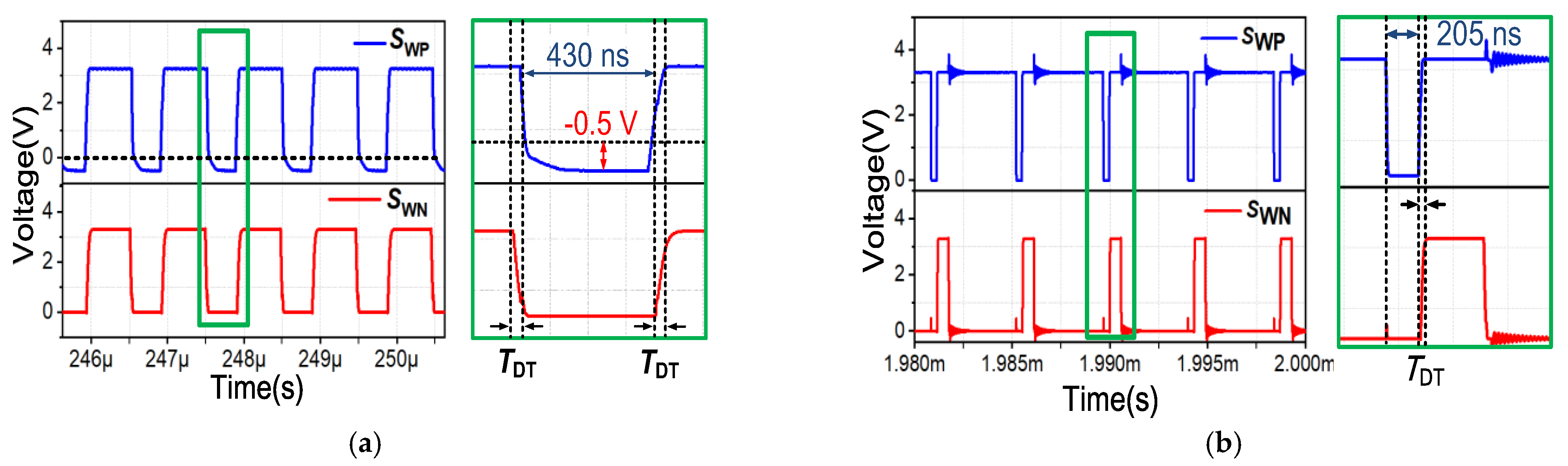
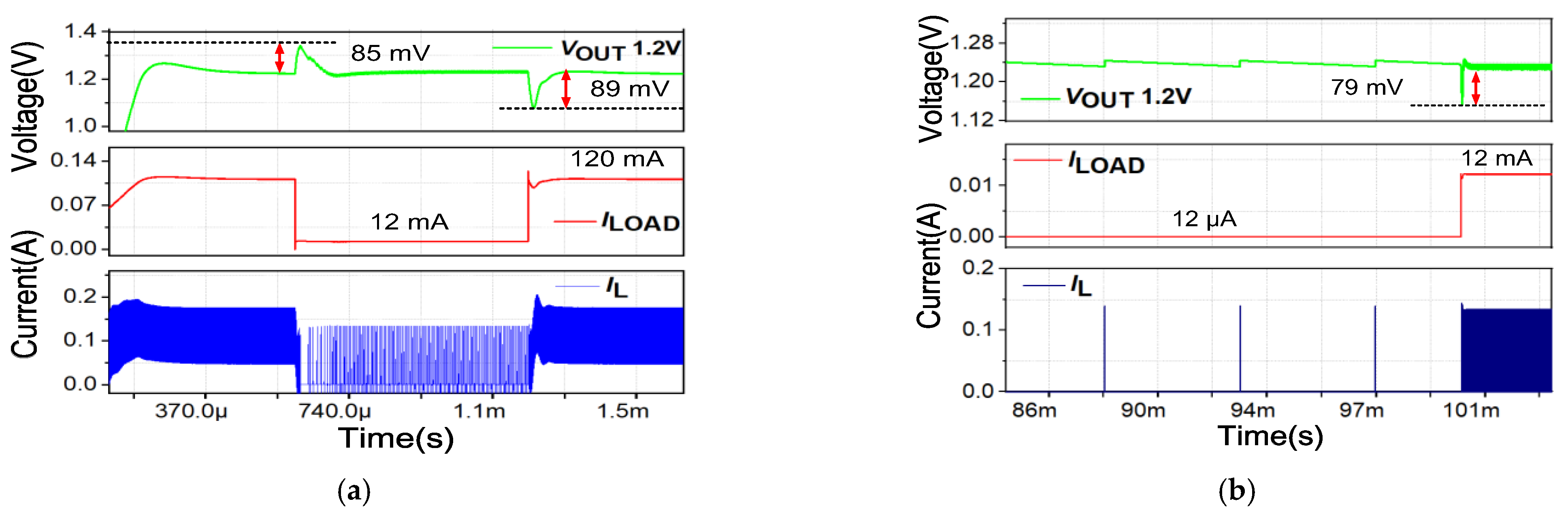
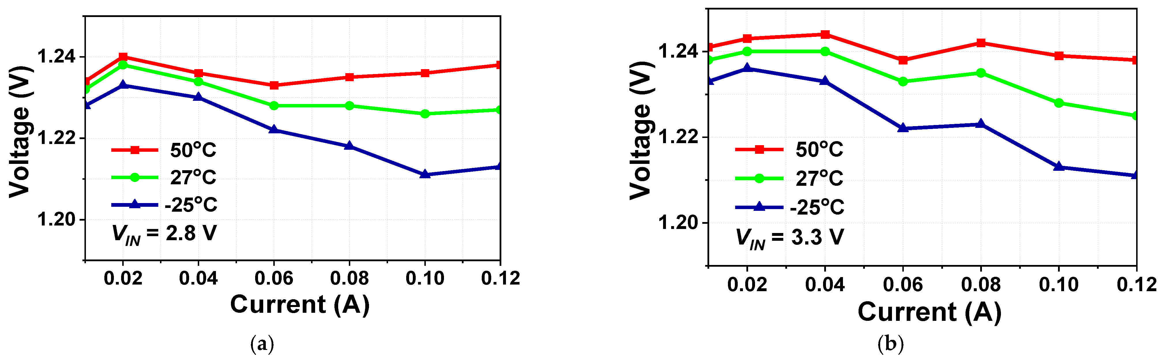
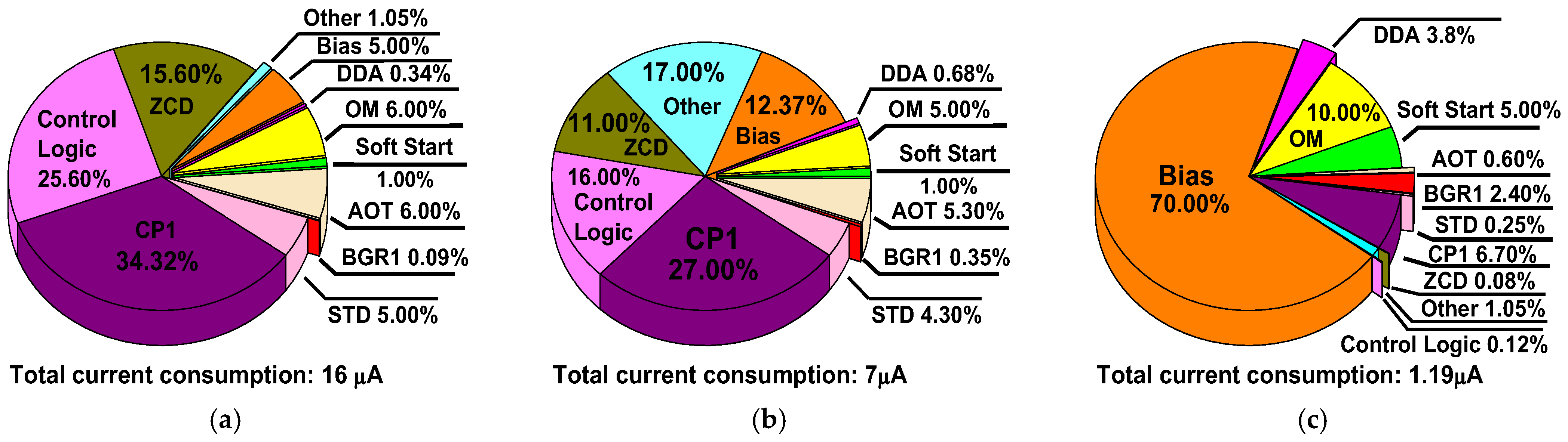
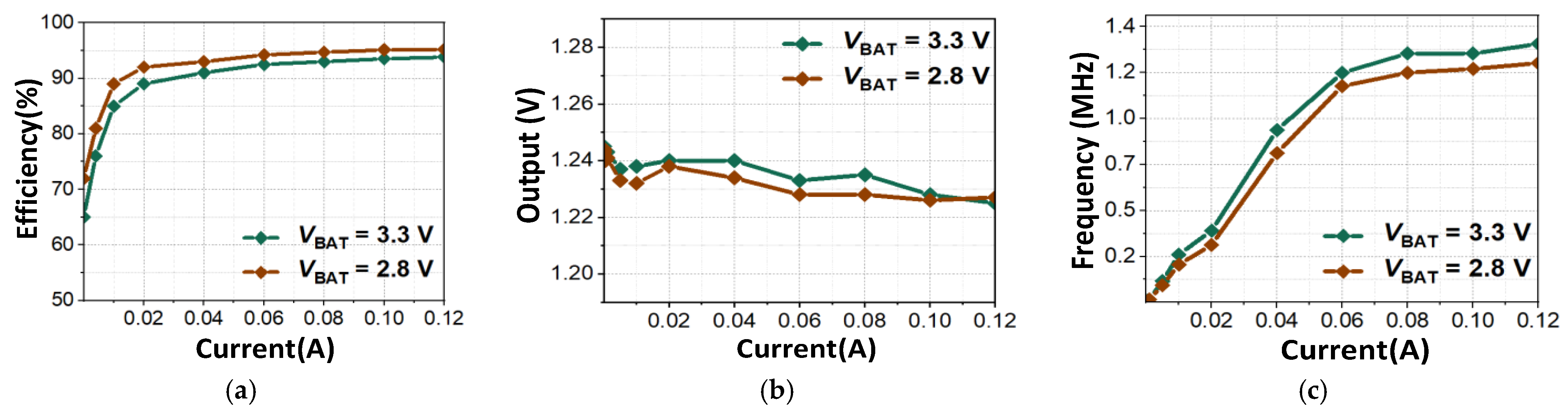
3. Simulation Results
4. Conclusions
Author Contributions
Funding
Data Availability Statement
Conflicts of Interest
References
- Blaauw, D.; Sylvester, D.; Dutta, P.; Lee, Y.; Lee, I.; Bang, S.; Kim, Y.; Kim, G.; Pannuto, P.; Kuo, Y.-S. IoT design space challenges: Circuits and systems. In Proceedings of the 2014 Symposium on VLSI Technology (VLSI-Technology): Digest of Technical Papers, Honolulu, HI, USA, 9–12 June 2014; pp. 1–2. [Google Scholar] [CrossRef]
- Roy, A.; Klinefelter, A.; Yahya, F.B.; Chen, X.; Gonzalez-Guerrero, L.P.; Lukas, C.J.; Kamakshi, D.A.; Boley, J.; Craig, K.; Faisal, M.; et al. A 6.45 µW Self-Powered SoC With Integrated Energy-Harvesting Power Management and ULP Asymmetric Radios for Portable Biomedical Systems. IEEE Trans. Biomed. Circuits Syst. 2015, 9, 862–874. [Google Scholar] [CrossRef] [PubMed]
- Pham, X.T.; Vu, T.K.; Nguyen, T.D.; Pham-Nguyen, L. A 1.2-µW 41-dB Ripple Attenuation Chopper Amplifier Using Auto-Zero Offset Cancelation Loop for Area-Efficient Biopotential Sensing. Electronics 2022, 11, 1149. [Google Scholar] [CrossRef]
- Pham, X.T.; Bo, Q.B.; Hoang, M.K.; Le, V.T.; Pham-Nguyen, L. 1.2 µW 41dB Ripple Attenuation Chopper Instrumentation Amplifier Using Auto-Zero Offset Cancellation Loop. In Proceedings of the 2021 International Conference on Advanced Technologies for Communications (ATC), Ho Chi Minh City, Vietnam, 14–16 October 2021; pp. 167–171. [Google Scholar] [CrossRef]
- Texas Instruments. 3 Quiescent-Current (Iq) Specifications to Understand. Technical Article SSZT118, November 2021. Available online: https://www.ti.com/document-viewer/lit/html/sszt118 (accessed on 1 January 2022).
- Poongan, B.; Rajendran, J.; Yizhi, L.; Mariappan, S.; Parameswaran, P.; Kumar, N.; Othman, M.; Nathan, A. A 53-µA-Quiescent 400-mA Load Demultiplexer Based CMOS Multi-Voltage Domain Low Dropout Regulator for RF Energy Harvester. Micromachines 2023, 14, 379. [Google Scholar] [CrossRef] [PubMed]
- Aguillon-Garcia, J.; Bañuelos-Sanchez, P. High-Efficiency DC-DC Converter for Large Input-Voltage Fluctuations in Solar Applications. Chin. J. Electron. 2015, 24, 502–507. [Google Scholar] [CrossRef]
- Chen, W.-C.; Ming, D.-L.; Su, Y.-P.; Lee, Y.-H.; Chen, K.-H. A Wide Load Range and High Efficiency Switched-Capacitor DC-DC Converter with Pseudo-Clock Controlled Load-Dependent Frequency. IEEE Trans. Circuits Syst. I 2014, 61, 911–921. [Google Scholar] [CrossRef]
- Hong, S.-W.; Park, S.-H.; Kong, T.-H.; Cho, G.-H. Inverting Buck-Boost DC-DC Converter for Mobile AMOLED Display Using Real-Time Self-Tuned Minimum Power-Loss Tracking (MPLT) Scheme with Lossless Soft-Switching for Light and Ultra-Light Load Mode. IEEE J. Solid-State Circuits 2015, 50, 2380–2393. [Google Scholar] [CrossRef]
- Wibben, J.; Harjani, R. A High-Efficiency DC–DC Converter Using 2 nH Integrated Inductors. IEEE J. Solid-State Circuits 2008, 43, 844–854. [Google Scholar] [CrossRef]
- Lee, C.-S.; Kim, S.-S.; Yu, J.-H. Load and Frequency Dependent CMOS Dual-Mode DC-DC Converter. Microelectron. J. 2019, 92, 104610. [Google Scholar] [CrossRef]
- Yuan, B.; Liu, M.-X.; Ng, W.T.; Lai, X.-Q. Hybrid Buck Converter with Constant Mode Changing Point and Smooth Mode Transition for High-Frequency Applications. IEEE Trans. Ind. Electron. 2020, 67, 1466–1474. [Google Scholar] [CrossRef]
- Kim, S.J.; Choi, W.-S.; Pilawa-Podgurski, R.; Hanumolu, P.K. A 10-MHz 2–800-mA 0.5–1.5-V 90% Peak Efficiency Time-Based Buck Converter with Seamless Transition Between PWM/PFM Modes. IEEE J. Solid-State Circuits 2018, 53, 814–824. [Google Scholar] [CrossRef]
- Chen, P.H.; Wu, C.S.; Lin, K.C. A 50 nW-to-10 mW Output Power Tri-Mode Digital Buck Converter with Self-Tracking Zero Current Detection for Photovoltaic Energy Harvesting. IEEE J. Solid-State Circuits 2016, 51, 523–532. [Google Scholar] [CrossRef]
- Shi, L.-F.; Jia, W.-G. Mode-Selectable High-Efficiency Low-Quiescent-Current Synchronous Buck DC–DC Converter. IEEE Trans. Ind. Electron. 2014, 61, 2278–2285. [Google Scholar] [CrossRef]
- Li, Y.; Zhu, Z. A Constant Current Control Scheme for Primary-Side Controlled Flyback Controller Operating in DCM and CCM. IEEE Trans. Power Electron. 2020, 35, 9462–9470. [Google Scholar] [CrossRef]
- Zhang, S.; Zhao, M.; Wu, X.; Zhang, H. Dual-phase DC–DC Buck Converter with Light-Load Performance Enhancement for Portable Applications. IET Power Electron. 2018, 11, 719–726. [Google Scholar] [CrossRef]
- Nguyen, M.T.; Ha, T.P.; Pham, X.T.; Hoang, M.K. High-Efficiency Buck DC-DC Converter Using Automatic PWM/PFM Mode Control Based on Load Current Variation with Digital Soft Start. In Proceedings of the Electrical, Electronics, Mechanical and Systems Engineering Session of the 2023 International Research Conference of Sri Lanka Technology Campus, Colombo, Sri Lanka, 14–15 December 2023; pp. 310–317. Available online: https://repo.sltc.ac.lk/handle/1/427 (accessed on 14 December 2023).
- Kim, M.W.; Kim, J.J. A PWM/PFM Dual-Mode DC-DC Buck Converter with Load-Dependent Efficiency-Controllable Scheme for Multi-Purpose IoT Applications. Energies 2021, 14, 960. [Google Scholar] [CrossRef]
- Santoro, F.; Kuhn, R.; Gibson, N.; Rasera, N.; Tost, T.; Graeb, H.; Wicht, B.; Brederlow, R. A Hysteretic Buck Converter with 92.1% Maximum Efficiency Designed for Ultra-Low Power and Fast Wake-Up SoC Applications. IEEE J. Solid-State Circuits 2018, 53, 1856–1868. [Google Scholar] [CrossRef]
- Huang, T.-C.; Hsieh, C.-Y.; Yang, Y.-Y.; Lee, Y.-H.; Kang, Y.-C.; Chen, K.-H.; Huang, C.-C.; Lin, Y.-H.; Lee, M.-W. A Battery-Free 217 nW Static Control Power Buck Converter for Wireless RF Energy Harvesting with α-Calibrated Dynamic on/off Time and Adaptive Phase Lead Control. IEEE J. Solid-State Circuits 2012, 47, 852–862. [Google Scholar] [CrossRef]
- Zheng, L.; Song, Z.; Guo, P.; Guo, J.; Chang, C.; Huang, P.; Lu, L. An Ultra-low Quiescent Current Tri-mode DC–DC Boost Converter with 95.6% Peak Efficiency for Internet of Things Application. IET Power Electron. 2023, 16, 1527–1537. [Google Scholar] [CrossRef]
- Gao, S.; Zhang, F.; Mei, H. Optimization Control Strategy for Light Load Efficiency of Four-Switch Buck-Boost Converter. World Electr. Veh. J. 2024, 15, 469. [Google Scholar] [CrossRef]
- Asano, H.; Hirose, T.; Kojima, Y.; Kuroki, N.; Numa, M. A Fully Integrated, Wide-Load-Range, High-Power-Conversion-Efficiency Switched Capacitor DC–DC Converter with Adaptive Bias Comparator for Ultra-Low-Power Power Management Integrated Circuit. Jpn. J. Appl. Phys. 2018, 57, 04FF03. [Google Scholar] [CrossRef]
- Hosseini, S.R.; Saberi, M.; Lotfi, R. A High-Speed and Power-Efficient Voltage Level Shifter for Dual-Supply Applications. IEEE Trans. Very Large Scale Integr. (VLSI) Syst. 2017, 25, 1154–1158. [Google Scholar] [CrossRef]
- Chandrasekhar, C.; Basha, M.M.; Das, S.M.; Hemakesavulu, O.; Dholvan, M.; Syed, J. Pass-Transistor-Enabled Split Input Voltage Level Shifter for Ultra-Low-Power Applications. Micromachines 2025, 16, 64. [Google Scholar] [CrossRef] [PubMed]
- Lee, B.; Ma, D.B. A 20 MHz On-Chip All-NMOS 3-Level DC-DC Converter with Interception Coupling Dead-Time Control and 3-Switch Bootstrap Gate Driver. IEEE Trans. Ind. Electron. 2021, 68, 6339–6347. [Google Scholar] [CrossRef]
- Liu, Z.; Cong, L.; Lee, H. Design of On-Chip Gate Drivers with Power-Efficient High-Speed Level Shifting and Dynamic Timing Control for High-Voltage Synchronous Switching Power Converters. IEEE J. Solid-State Circuits 2015, 50, 1463–1477. [Google Scholar] [CrossRef]
- Yuan, B.; Ying, J.; Ng, W.T.; Lai, X.-Q.; Zhang, L.-F. A High-Voltage DC–DC Buck Converter with Dynamic Level Shifter for Bootstrapped High-Side Gate Driver and Diode Emulator. IEEE Trans. Power Electron. 2020, 35, 7295–7304. [Google Scholar] [CrossRef]
- Park, Y.-J.; Park, J.-H.; Kim, H.-J.; Ryu, H.; Kim, S.; Pu, Y.; Hwang, K.C.; Yang, Y.; Lee, M.; Lee, K.-Y. A Design of a 92.4% Efficiency Triple Mode Control DC–DC Buck Converter with Low Power Retention Mode and Adaptive Zero Current Detector for IoT/Wearable Applications. IEEE Trans. Power Electron. 2017, 32, 6946–6960. [Google Scholar] [CrossRef]
- Cheng, L.; Tang, K.; Ki, W.-H.; Su, F. Fast-Transient Techniques for High-Frequency DC–DC Converters. J. Semicond. 2020, 41, 112402. [Google Scholar] [CrossRef]
- Nguyen-Thien, V.; Han, H.-D.; Pham-Nguyen, L.; Pham, X.T.; Hoang, M.K. 0.47-μW Multi-Stage Low Noise Amplifier Employing 0.2-V-Supply OTA. In Proceedings of the 2022 IEEE Ninth International Conference on Communications and Electronics (ICCE), Nha Trang, Vietnam, 27–29 July 2022; pp. 190–194. [Google Scholar] [CrossRef]
- Chauhan, S.; Mehra, R. CMOS Design and Performance Analysis of Ring Oscillator for Different Stages. Int. J. Eng. Trends Technol. 2016, 32, 234–237. [Google Scholar] [CrossRef]
- Lee, C.; Yim, T.; Yoon, H. A Negative Charge Pump Using Enhanced Pumping Clock for Low-Voltage DRAM. Electronics 2020, 9, 1769. [Google Scholar] [CrossRef]
- Tyagi, V.; Kalla, S.; Rana, V. Negative Voltage Generator and Current DAC Based Regulator for Flash Memory. In Proceedings of the 2021 34th International Conference on VLSI Design and 2021 20th International Conference on Embedded Systems (VLSID), Guwahati, India, 20–24 February 2021; pp. 17–22. [Google Scholar] [CrossRef]
- Zhaoxia, L.; Qingfeng, L.; Jinkun, S.; Jian, L. A research of efficiency characteristic for Buck converter. In Proceedings of the 2010 the 2nd International Conference on Industrial Mechatronics and Automation, Wuhan, China, 30–31 May 2010; pp. 232–235. [Google Scholar] [CrossRef]
- Liu, J.-M.; Wang, P.-Y.; Kuo, T.-H. A Current-Mode DC–DC Buck Converter with Efficiency-Optimized Frequency Control and Reconfigurable Compensation. IEEE Trans. Power Electron. 2012, 27, 869–880. [Google Scholar] [CrossRef]
- Park, W.; Namgoong, G.; Choi, E.; Lee, B.; Park, H.; Ma, H.; Bien, F. A 94% Peak Efficiency Dual Mode Buck Converter with Fully Integrated On-Time-Based Mode Control for Implantable Medical Devices. IEEE Trans. Circuits Syst. II 2022, 69, 4458–4462. [Google Scholar] [CrossRef]
- Zhang, Z.; Shi, H.; Lu, D.; Cao, P.; Hong, Z. An AOT Buck Converter with Adaptive TON Extender Achieving 2.5 µs Settling Time in 4A Load Transient. In Proceedings of the 2022 IEEE International Conference on Integrated Circuits, Technologies and Applications (ICTA), Xi’an, China, 28–30 October 2022; pp. 176–177. [Google Scholar] [CrossRef]
- Yu, J.; Hwang, I.; Kim, N. High performance CMOS integrated PWM/PFM dual-mode DC-DC buck converter. In Proceedings of the 2017 18th International Scientific Conference on Electric Power Engineering (EPE), Kouty nad Desnou, Czech Republic, 17–19 May 2017; pp. 1–4. [Google Scholar] [CrossRef]
- Jiang, C.; Chai, C.; Han, C.; Yang, Y. A High Performance Adaptive On-Time Controlled Valley-Current-Mode DC–DC Buck Converter. J. Semicond. 2020, 41, 062402. [Google Scholar] [CrossRef]


| Condition | Output Voltage (V) | Output Ripple (mV) | Frequency (kHz) | Efficiency (%) | Load (mA) | TSLEEP (μs) | Input Voltage (V) |
|---|---|---|---|---|---|---|---|
| Heavy load | 1.24 | 3 | 1300 | 93.35 | 120 | 0 | 3.3 |
| Light load | 1.235 | 7 | 260 | 88 | 12 | 3.7 | |
| 1.23 | 10 | 30 | 83 | 1.2 | 30 | ||
| Ultra light load | 1.228 | 12 | 0.27 | 65 | 0.012 | 3800 | |
| Heavy load | 1.231 | 2.8 | 1230 | 96.2 | 120 | 0 | 2.8 |
| Light load | 1.23 | 6.5 | 230 | 94 | 12 | 3.6 | |
| 1.228 | 9.2 | 28 | 89 | 1.2 | 28.5 | ||
| Ultra light load | 1.225 | 11.5 | 0.25 | 72 | 0.012 | 3750 |
| Parameter | [20] | [30] | [38] | [39] | [40] | [41] | This Work |
|---|---|---|---|---|---|---|---|
| Result | Meas. | Meas. | Meas. | Sim. | Sim. | Sim. | Sim. |
| Num. of Control | 1 | 3 | 2 | 1 | 2 | 1 | 1 |
| Operation Modes | AOT | PWM/PFM/RM | PWM/ PFM | AOT | PWM/ PFM | AOT | AOT |
| Process (μm) | 0.13 | 0.13 | 0.18 | 0.18 | 0.18 | 0.18 | 0.18 |
| Input Voltage (V) | 1.8–3.3 | 2.2–3.3 | 2.2–5 | 5–12 | 3.3–5 | 5 | 2.8–3.3 |
| Output Voltage (V) | 1.2 | 1.7 | 1.8 | 0.33–1.2 | 0.5–3 | 1.2 | 1.2 |
| Inductor (μH) | 4.7 | 3 | 4.7 | 2.2 | 500–3000 | 1.5 | 4.7 |
| Output Capacitor (μF) | 4.7 | 3 | 1 | 47 | 50–200 | 20 | 4.7 |
| Output Ripple Max (mV) | 30 | 180 | N/A | N/A | N/A | 5 | 3 |
| ILOAD Max (mA) | 0.0001–2.65 | 0.01–20 | 0.2–200 | 5000 | 200 | 500 | 0.012–120 |
| Efficiency (@12 μA) (%) | 62 | 74.2 | 77 | N/A | N/A | 40 | 73 |
| Peak Efficiency (%) | 92.2 | 92.4 | 94 | 96 | 90 | 95 | 96.2 |
| Chip Area (mm2) | 0.14 | 1.1 | 0.405 | N/A | N/A | N/A | 0.31 |
Disclaimer/Publisher’s Note: The statements, opinions and data contained in all publications are solely those of the individual author(s) and contributor(s) and not of MDPI and/or the editor(s). MDPI and/or the editor(s) disclaim responsibility for any injury to people or property resulting from any ideas, methods, instructions or products referred to in the content. |
© 2025 by the authors. Licensee MDPI, Basel, Switzerland. This article is an open access article distributed under the terms and conditions of the Creative Commons Attribution (CC BY) license (https://creativecommons.org/licenses/by/4.0/).
Share and Cite
Pham, X.T.; Nguyen, M.T.; Pham, C.-K.; Thuc, K.-X. Buck Converter with Improved Efficiency and Wide Load Range Enabled by Negative Level Shifter and Low-Power Adaptive On-Time Controller. Electronics 2025, 14, 2425. https://doi.org/10.3390/electronics14122425
Pham XT, Nguyen MT, Pham C-K, Thuc K-X. Buck Converter with Improved Efficiency and Wide Load Range Enabled by Negative Level Shifter and Low-Power Adaptive On-Time Controller. Electronics. 2025; 14(12):2425. https://doi.org/10.3390/electronics14122425
Chicago/Turabian StylePham, Xuan Thanh, Minh Tan Nguyen, Cong-Kha Pham, and Kieu-Xuan Thuc. 2025. "Buck Converter with Improved Efficiency and Wide Load Range Enabled by Negative Level Shifter and Low-Power Adaptive On-Time Controller" Electronics 14, no. 12: 2425. https://doi.org/10.3390/electronics14122425
APA StylePham, X. T., Nguyen, M. T., Pham, C.-K., & Thuc, K.-X. (2025). Buck Converter with Improved Efficiency and Wide Load Range Enabled by Negative Level Shifter and Low-Power Adaptive On-Time Controller. Electronics, 14(12), 2425. https://doi.org/10.3390/electronics14122425