
Model-Based Design of Contrast-Limited Histogram Equalization for Low-Complexity, High-Speed, and Low-Power Tone-Mapping Operation

Abstract
1. Introduction
2. Apparatus and Methods
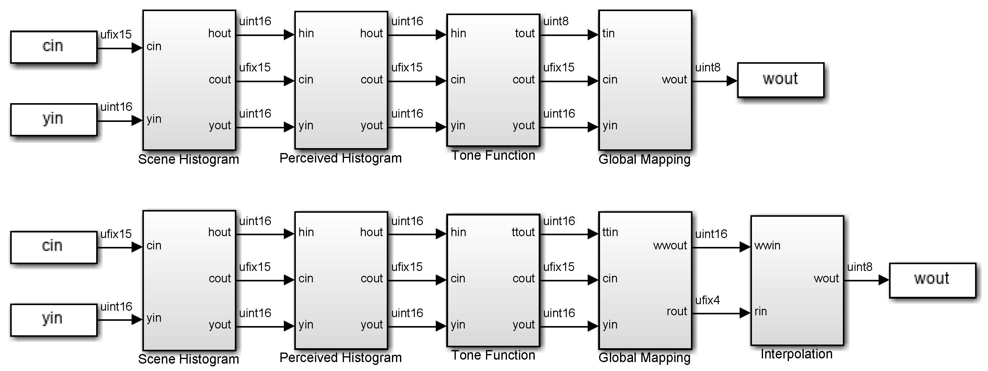
2.1. Design Overview
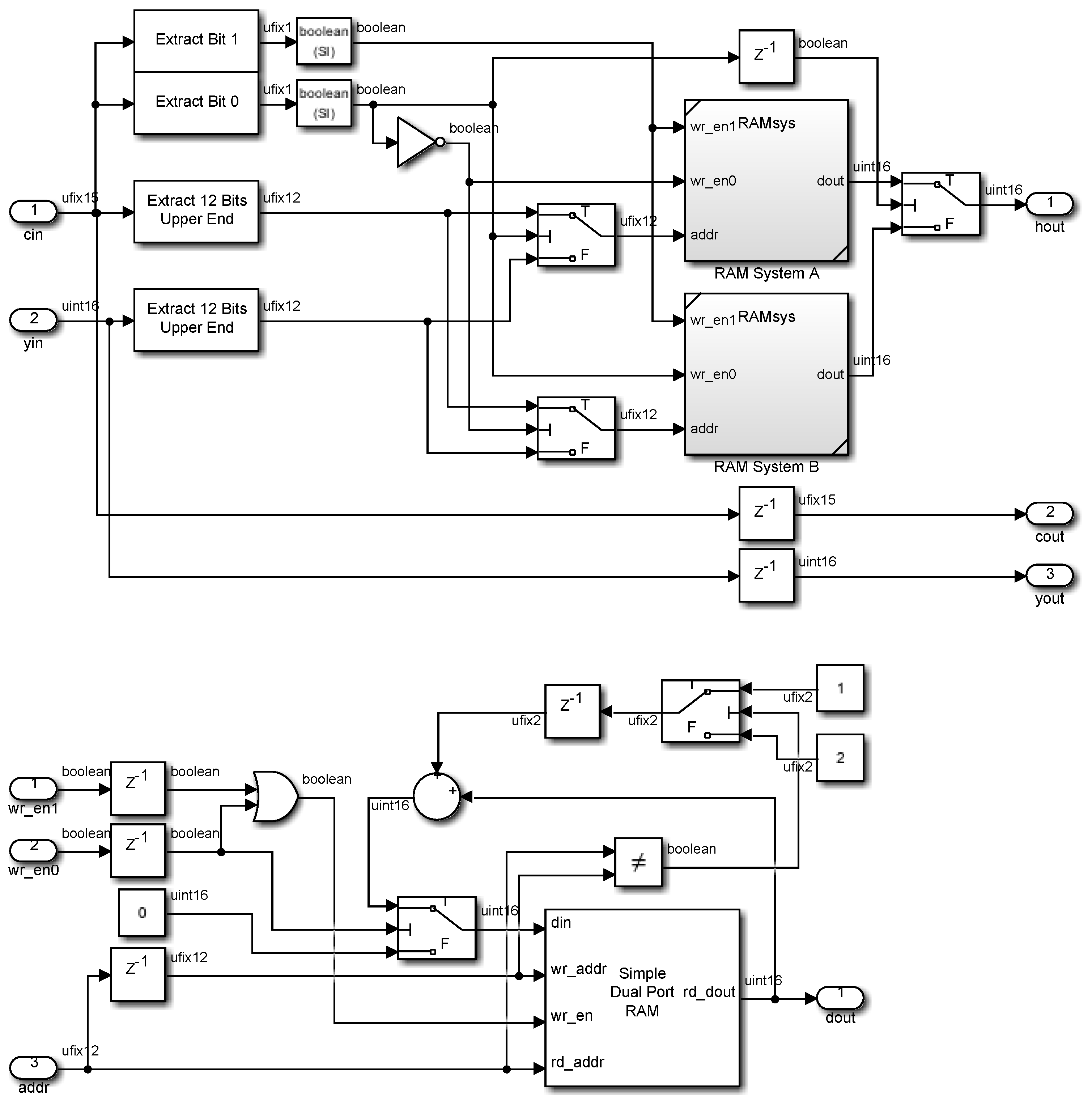
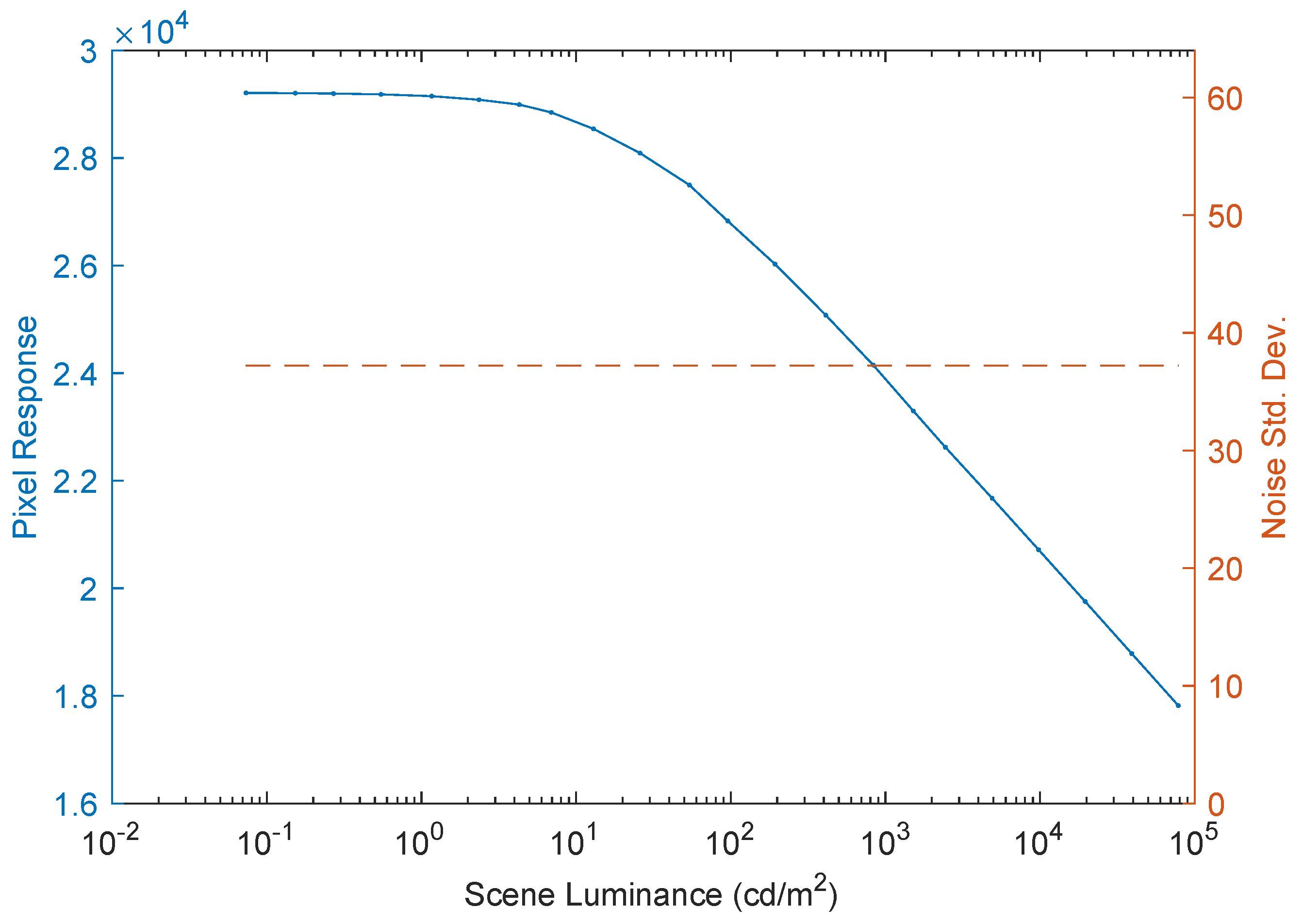
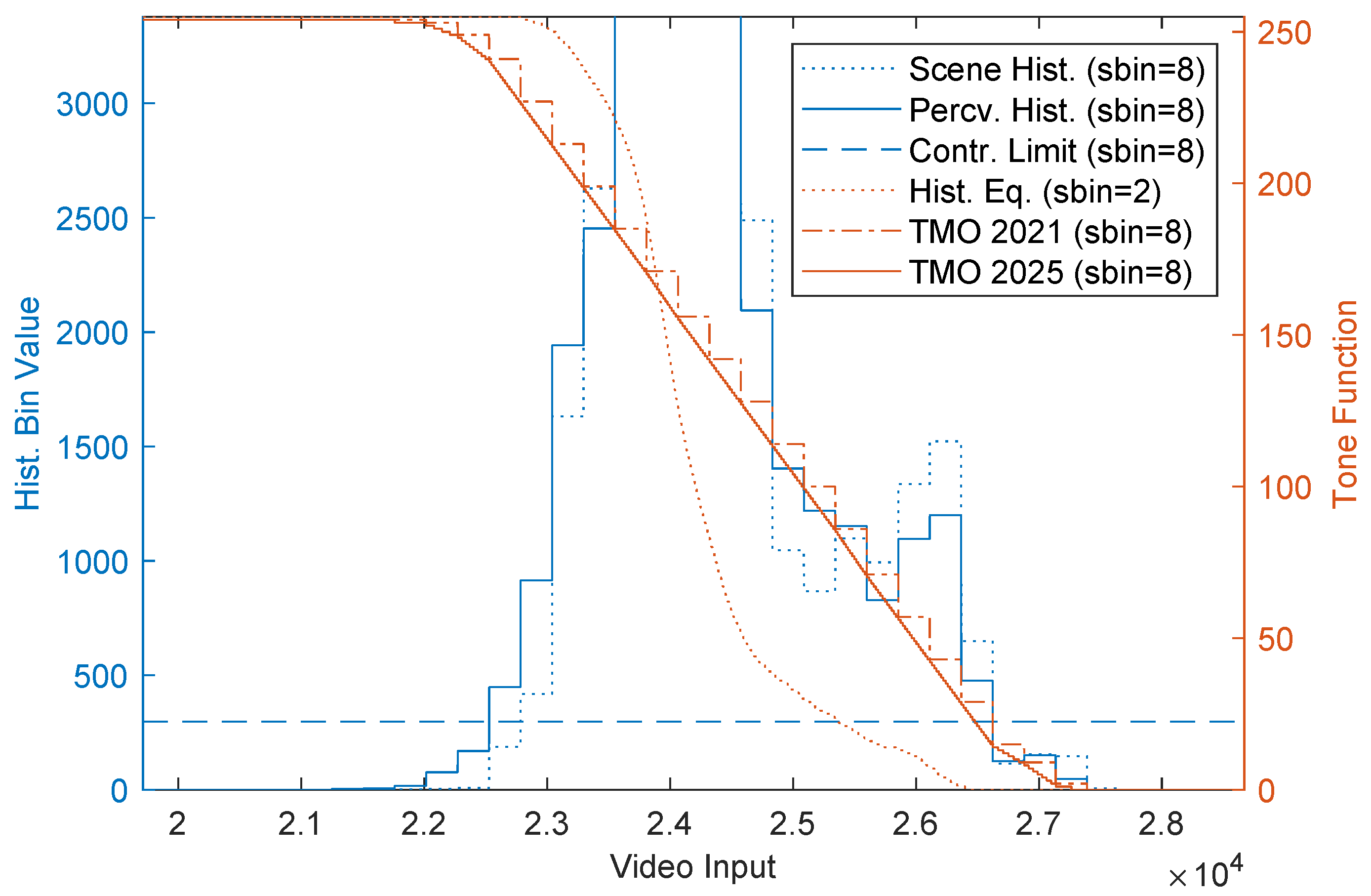
2.2. Scene Histogram
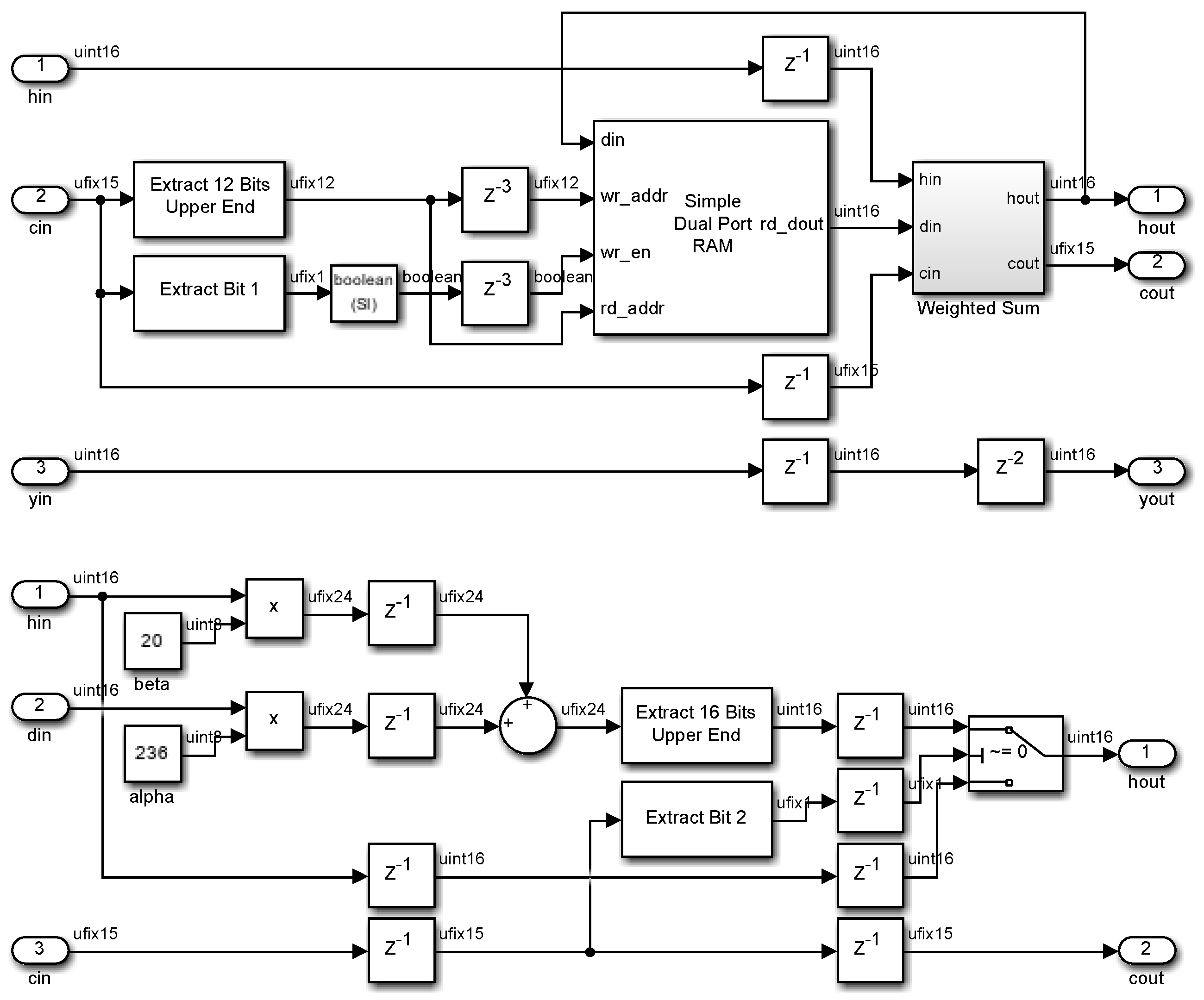
2.3. Perceived Histogram
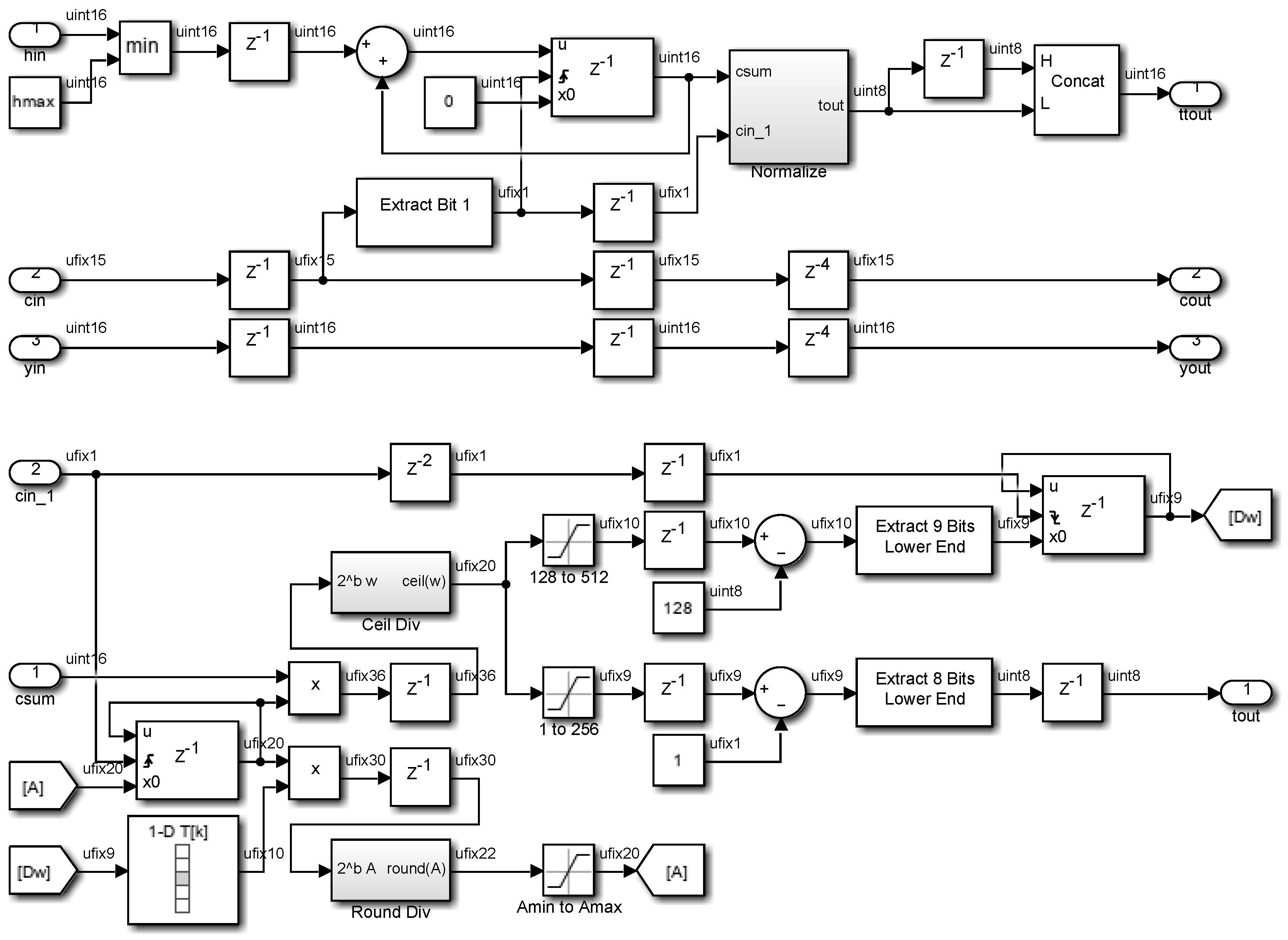
2.4. Tone Function
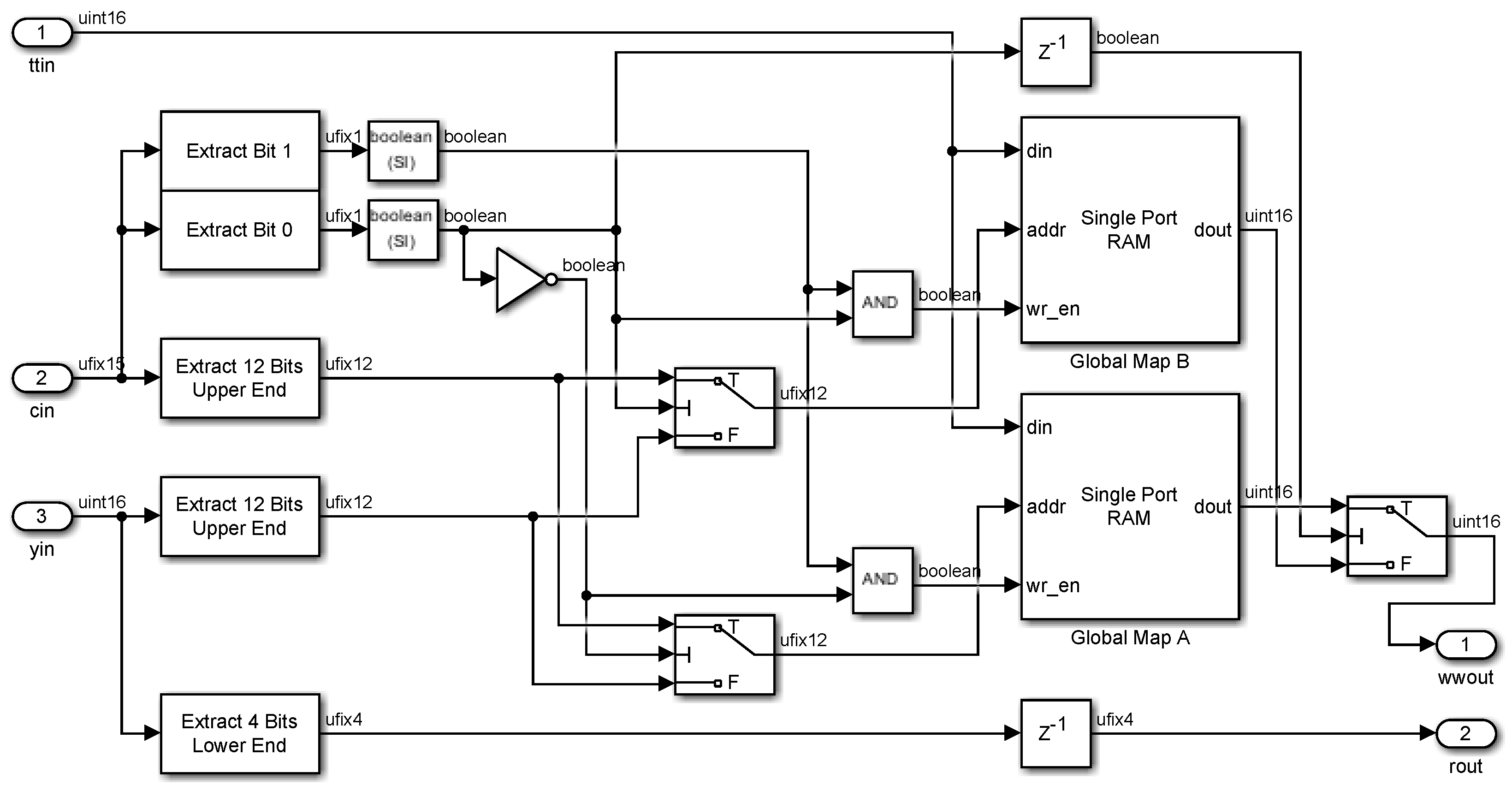
2.5. Global Mapping
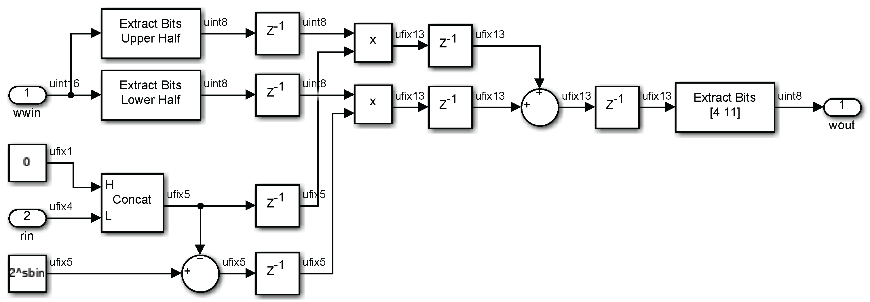
2.6. Interpolation
3. Results and Discussion
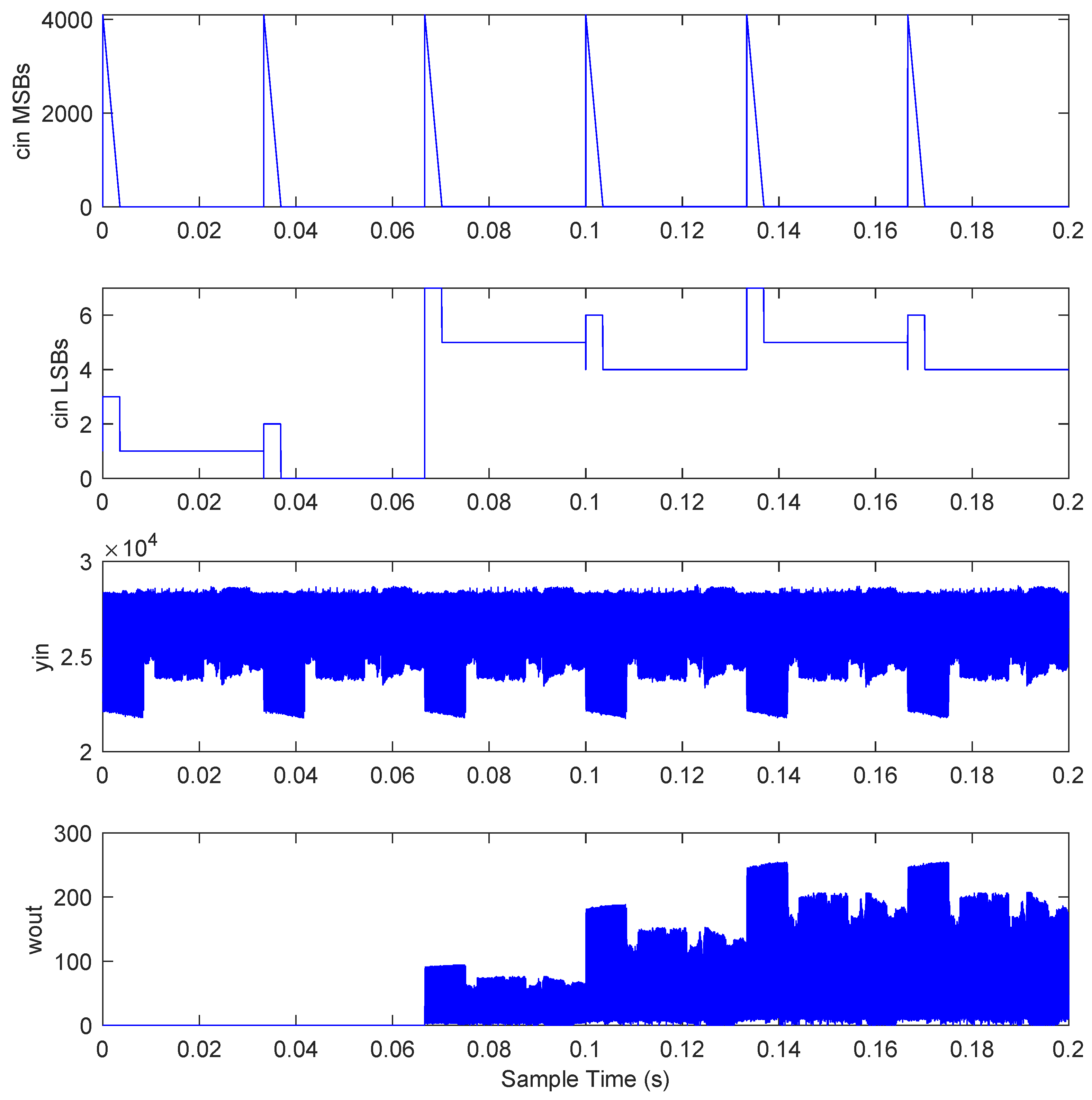
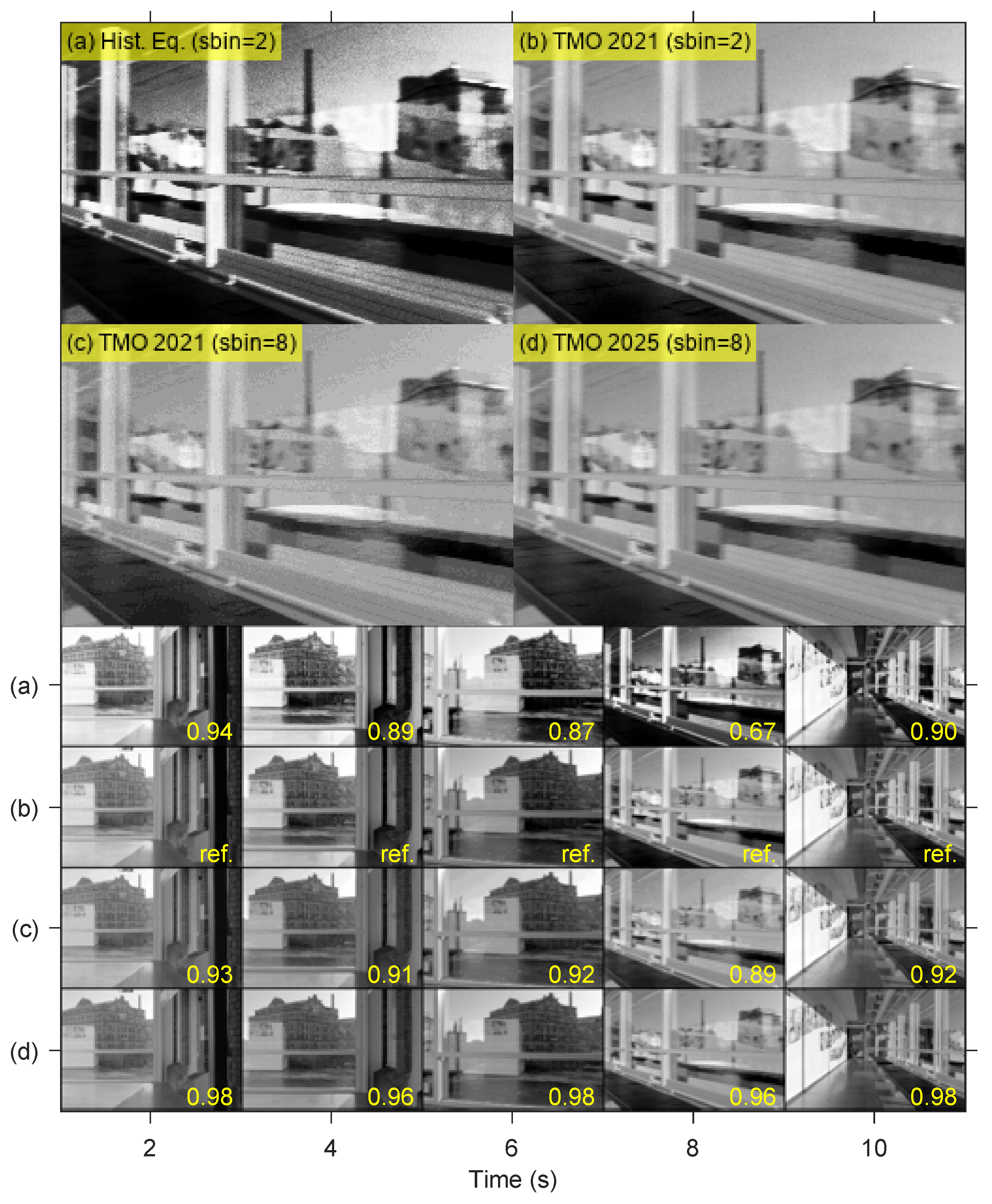
3.1. Verification
3.2. Evaluation
4. Conclusions
Author Contributions
Funding
Data Availability Statement
Acknowledgments
Conflicts of Interest
Abbreviations
| 4KUHD | 4K ultra HD |
| AMD | Advanced Micro Devices |
| APS | active pixel sensor |
| cd/m2 | candelas per metre squared |
| CMOS | complementary metal-oxide-semiconductor |
| dB | decibels |
| DPS | digital pixel sensor |
| FHD | full HD |
| FPGA | field-programmable gate array |
| fps | frames per second |
| GPU | graphics processing unit |
| HD | high-definition |
| HDL | hardware-description language |
| HDR | high-dynamic-range |
| HQVGA | half-quarter VGA |
| HVS | human visual system |
| ISE | Integrated Synthesis Environment |
| Kb | bits |
| LDR | low-dynamic-range |
| log | logarithmic |
| LPF | low-pass filter |
| LSB | least-significant bit |
| LUT | look-up table |
| MHz | megahertz |
| MSB | most-significant bit |
| mW | milliwatts |
| ns | nanoseconds |
| RAM | random-access memory |
| s | seconds |
| SD | standard-definition |
| SoC | system-on-chip |
| SSim | structural similarity |
| STA | static timing analysis |
| TMO | tone-mapping operator |
| VGA | video-graphics-array |
| VHDL | very-high-speed integrated-circuit HDL |
References
- Takayanagi, I.; Kuroda, R. HDR CMOS Image Sensors for Automotive Applications. IEEE Trans. Electron Devices 2022, 69, 2815–2823. [Google Scholar] [CrossRef]
- Brunetti, A.M.; Choubey, B. A Low Dark Current 160 dB Logarithmic Pixel with Low Voltage Photodiode Biasing. Electronics 2021, 10, 1096. [Google Scholar] [CrossRef]
- Hajisharif, S.; Kronander, J.; Unger, J. Adaptive dualISO HDR reconstruction. EURASIP J. Image Video Process. 2015, 2015, 41. [Google Scholar] [CrossRef]
- Khan, I.R.; Rahardja, S.; Khan, M.M.; Movania, M.M.; Abed, F. A Tone-Mapping Technique Based on Histogram Using a Sensitivity Model of the Human Visual System. IEEE Trans. Ind. Electron. 2018, 65, 3469–3479. [Google Scholar] [CrossRef]
- Völgyes, D.; Martinsen, A.C.T.; Stray-Pedersen, A.; Waaler, D.; Pedersen, M. A Weighted Histogram-Based Tone Mapping Algorithm for CT Images. Algorithms 2018, 11, 111. [Google Scholar] [CrossRef]
- Larson, G.W.; Rushmeier, H.; Piatko, C. A Visibility Matching Tone Reproduction Operator for High Dynamic Range Scenes. IEEE Trans. Vis. Comput. Graph. 1997, 3, 291–306. [Google Scholar] [CrossRef]
- Li, J.; Skorka, O.; Ranaweera, K.; Joseph, D. Novel Real-Time Tone-Mapping Operator for Noisy Logarithmic CMOS Image Sensors. J. Imaging Sci. Technol. 2016, 60, 020404. [Google Scholar] [CrossRef]
- Rana, A.; Valenzise, G.; Dufaux, F. Learning-Based Tone Mapping Operator for Efficient Image Matching. IEEE Trans. Multimed. 2019, 21, 256–268. [Google Scholar] [CrossRef]
- Gunawan, I.P.; Cloramidina, O.; Syafa’ah, S.B.; Febriani, R.H.; Kuntarto, G.P.; Santoso, B.I. A review on high dynamic range (HDR) image quality assessment. Int. J. Smart Sens. Intell. Syst. 2021, 14, 1–17. [Google Scholar] [CrossRef]
- Tade, S.L.; Vyas, V. Tone Mapped High Dynamic Range Image Quality Assessment Techniques: Survey and Analysis. Arch. Comput. Methods Eng. 2021, 28, 1561–1574. [Google Scholar] [CrossRef]
- Ou, Y.; Ambalathankandy, P.; Takamaeda, S.; Motomura, M.; Asai, T.; Ikebe, M. Real-Time Tone Mapping: A Survey and Cross-Implementation Hardware Benchmark. IEEE Trans. Circuits Syst. Video Technol. 2022, 32, 2666–2686. [Google Scholar] [CrossRef]
- Kashyap, S.; Giri, P.; Bhandari, A.K. Logarithmically Optimized Real-Time HDR Tone Mapping With Hardware Implementation. IEEE Trans. Circuits Syst. II Express Briefs 2024, 71, 1426–1430. [Google Scholar] [CrossRef]
- Muneer, M.H.; Pasha, M.A.; Khan, I.R. Hardware-friendly tone-mapping operator design and implementation for real-time embedded vision applications. Comput. Electr. Eng. 2023, 110, 108892. [Google Scholar] [CrossRef]
- Nascimento, M.; Li, J.; Joseph, D. Efficient Pipelined Circuits for Histogram-based Tone Mapping of Nonlinear CMOS Image Sensors. J. Imaging Sci. Technol. 2021, 65, 040503. [Google Scholar] [CrossRef]
- Xilinx. 7 Series: Product Selection Guide. Tech. Rep., Advanced Micro Devices, 2021. Available online: https://docs.amd.com/v/u/en-US/7-series-product-selection-guide (accessed on 19 March 2025).
- Xilinx. Zynq-7000 SoC: Product Selection Guide. Tech. Rep., Advanced Micro Devices, 2019. Available online: https://docs.amd.com/v/u/en-US/zynq-7000-product-selection-guide (accessed on 26 March 2025).
- Kronander, J.; Gustavson, S.; Bonnet, G.; Unger, J. Unified HDR reconstruction from raw CFA data. In Proceedings of the IEEE International Conference on Computational Photography, Cambridge, MA, USA, 19–21 April 2013; pp. 1–9. [Google Scholar] [CrossRef]
- Mahmoodi, A.; Li, J.; Joseph, D. Digital Pixel Sensor Array with Logarithmic Delta-Sigma Architecture. Sensors 2013, 13, 10765–10782. [Google Scholar] [CrossRef] [PubMed]
- Wang, Z.; Bovik, A.C.; Sheikh, H.R.; Simoncelli, E.P. Image Quality Assessment: From Error Visibility to Structural Similarity. IEEE Trans. Image Process. 2004, 13, 600–612. [Google Scholar] [CrossRef] [PubMed]
- Hai, J.C.T.; Pun, O.C.; Haw, T.W. Accelerating Video and Image Processing Design for FPGA using HDL Coder and Simulink. In Proceedings of the IEEE Conference on Sustainable Utilization and Development in Engineering and Technology, Selangor, Malaysia, 15–17 October 2015; pp. 28–32. [Google Scholar] [CrossRef]

| Video Format Acronym (Acronym Definition) | Number of Pixels, | Frame Rate, | Sample Rate, | Width of Histogram RAMs, |
|---|---|---|---|---|
| HQVGA (half-quarter VGA) | 30 fps | 1 MHz | 16 | |
| VGA (video-graphics-array) | 30 fps | 9 MHz | 19 | |
| HD (high-definition) | 30 fps | 28 MHz | 20 | |
| FHD (full HD) | 30 fps | 62 MHz | 21 | |
| 4KUHD (4K ultra HD) | 30 fps | 249 MHz | 23 |
| Video Format | System Design (Bin Size, Bits) | Logic Cells (Utilization) | Memory Bits (Utilization) | Maximum Frequency | Static Power | Dynamic Power |
|---|---|---|---|---|---|---|
| HQVGA | TMO 2021 (2) | 376 () | 1154 K () | 182 MHz | 61 mW | 1 mW |
| TMO 2021 (8) | 306 () | 91 K () | 164 MHz | 60 mW | 1 mW | |
| TMO 2025 (8) | 442 () | 92 K () | 120 MHz | 58 mW | 1 mW | |
| VGA | TMO 2021 (2) | 456 () | 1316 K () | 172 MHz | 61 mW | 12 mW |
| TMO 2021 (8) | 395 () | 92 K () | 164 MHz | 60 mW | 2 mW | |
| TMO 2025 (8) | 530 () | 92 K () | 119 MHz | 58 mW | 2 mW | |
| HD | TMO 2021 (2) | 539 () | 1424 K () | 169 MHz | 61 mW | 40 mW |
| TMO 2021 (8) | 467 () | 92 K () | 164 MHz | 60 mW | 7 mW | |
| TMO 2025 (8) | 603 () | 92 K () | 119 MHz | 58 mW | 7 mW | |
| FHD | TMO 2021 (2) | 525 () | 1478 K () | 169 MHz | 61 mW | 94 mW |
| TMO 2021 (8) | 501 () | 92 K () | 161 MHz | 60 mW | 15 mW | |
| TMO 2025 (8) | 637 () | 92 K () | 119 MHz | 58 mW | 17 mW | |
| 4KUHD | TMO 2021 (2) | 637 () | 1586 K () | 167 MHz | Max freq. | |
| TMO 2021 (8) | 565 () | 92 K () | 161 MHz | Max freq. | ||
| TMO 2025 (8) | 741 () | 92 K () | 119 MHz | Max freq. | ||
Disclaimer/Publisher’s Note: The statements, opinions and data contained in all publications are solely those of the individual author(s) and contributor(s) and not of MDPI and/or the editor(s). MDPI and/or the editor(s) disclaim responsibility for any injury to people or property resulting from any ideas, methods, instructions or products referred to in the content. |
© 2025 by the authors. Licensee MDPI, Basel, Switzerland. This article is an open access article distributed under the terms and conditions of the Creative Commons Attribution (CC BY) license (https://creativecommons.org/licenses/by/4.0/).
Share and Cite
Dong, W.; Nascimento, M.; Joseph, D. Model-Based Design of Contrast-Limited Histogram Equalization for Low-Complexity, High-Speed, and Low-Power Tone-Mapping Operation. Electronics 2025, 14, 2416. https://doi.org/10.3390/electronics14122416
Dong W, Nascimento M, Joseph D. Model-Based Design of Contrast-Limited Histogram Equalization for Low-Complexity, High-Speed, and Low-Power Tone-Mapping Operation. Electronics. 2025; 14(12):2416. https://doi.org/10.3390/electronics14122416
Chicago/Turabian StyleDong, Wei, Maikon Nascimento, and Dileepan Joseph. 2025. "Model-Based Design of Contrast-Limited Histogram Equalization for Low-Complexity, High-Speed, and Low-Power Tone-Mapping Operation" Electronics 14, no. 12: 2416. https://doi.org/10.3390/electronics14122416
APA StyleDong, W., Nascimento, M., & Joseph, D. (2025). Model-Based Design of Contrast-Limited Histogram Equalization for Low-Complexity, High-Speed, and Low-Power Tone-Mapping Operation. Electronics, 14(12), 2416. https://doi.org/10.3390/electronics14122416