
Differential-Fed Wideband Circularly Polarized SIW Cavity-Backed Slot Antenna Array


Abstract
1. Introduction
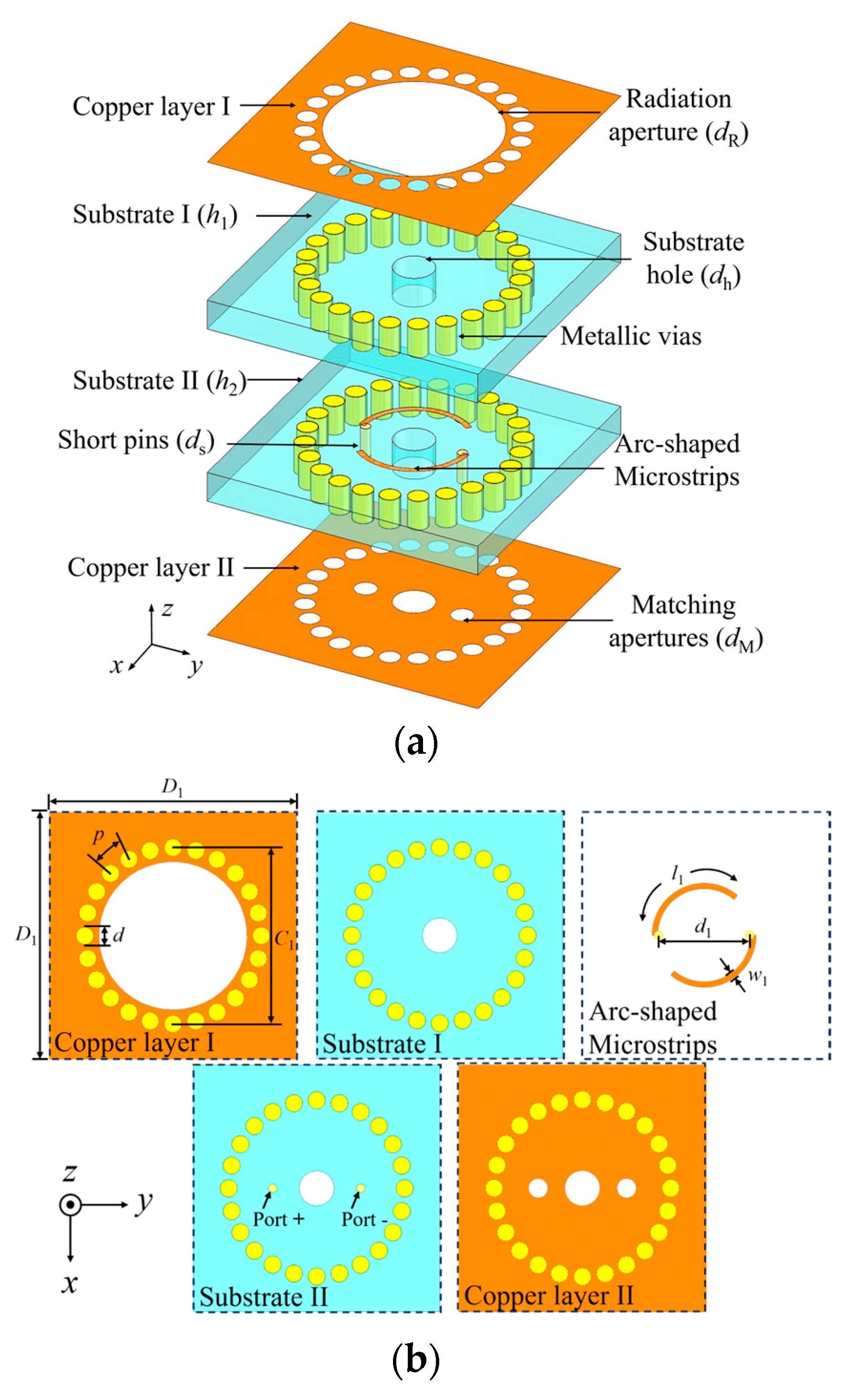
2. Antenna Element
2.1. Configuration
2.2. Evolution Process
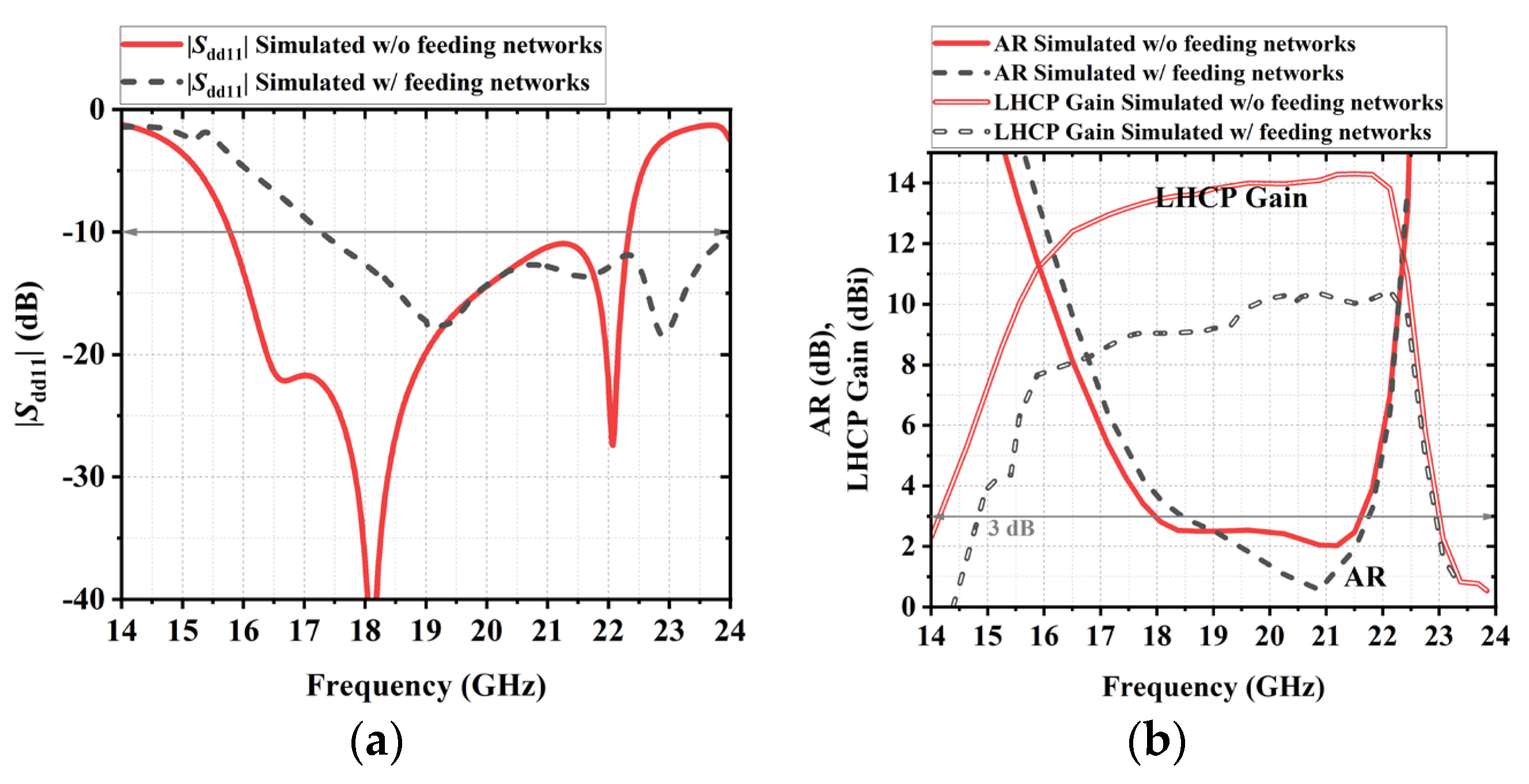
2.3. Working Principle
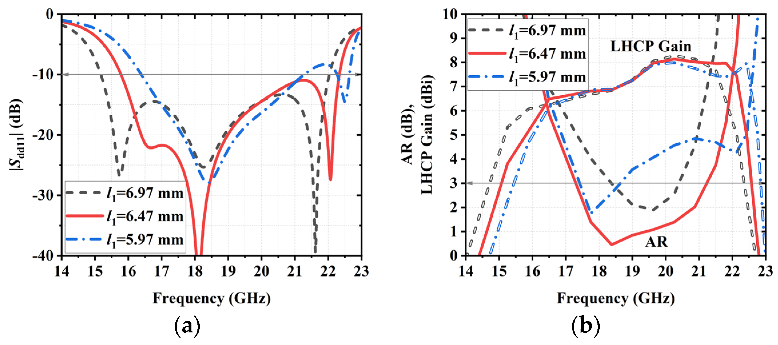
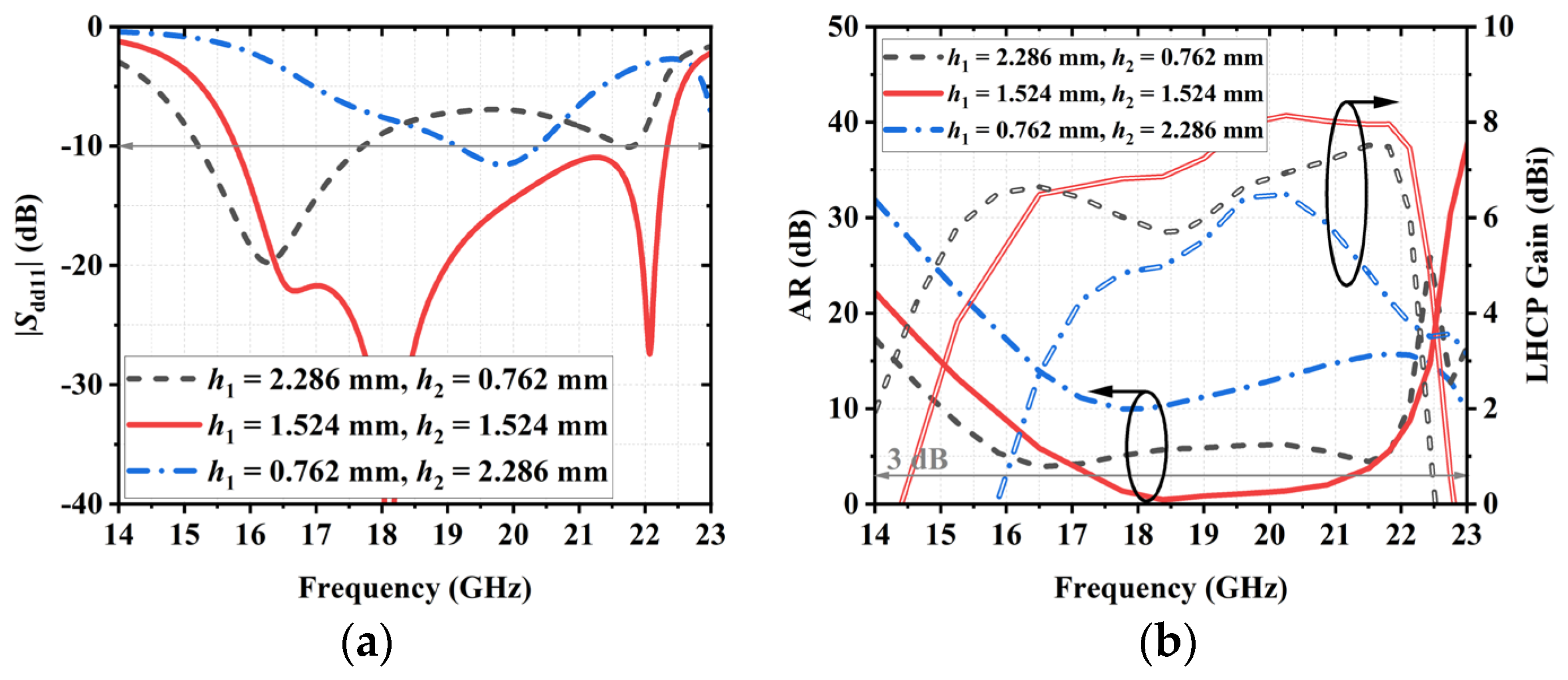
2.4. Parametric Study
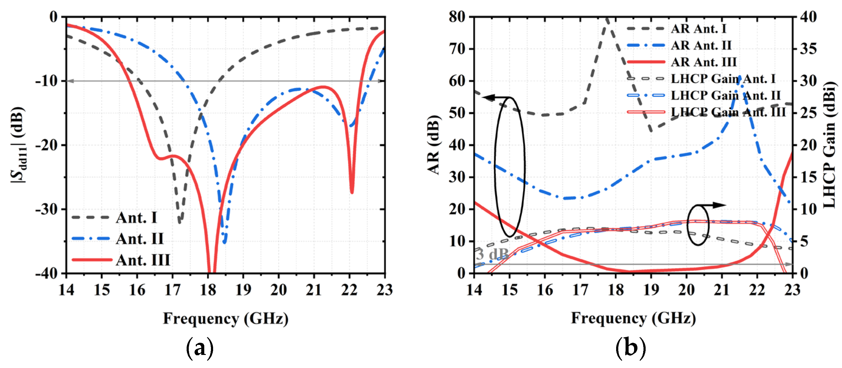
2.5. Performance
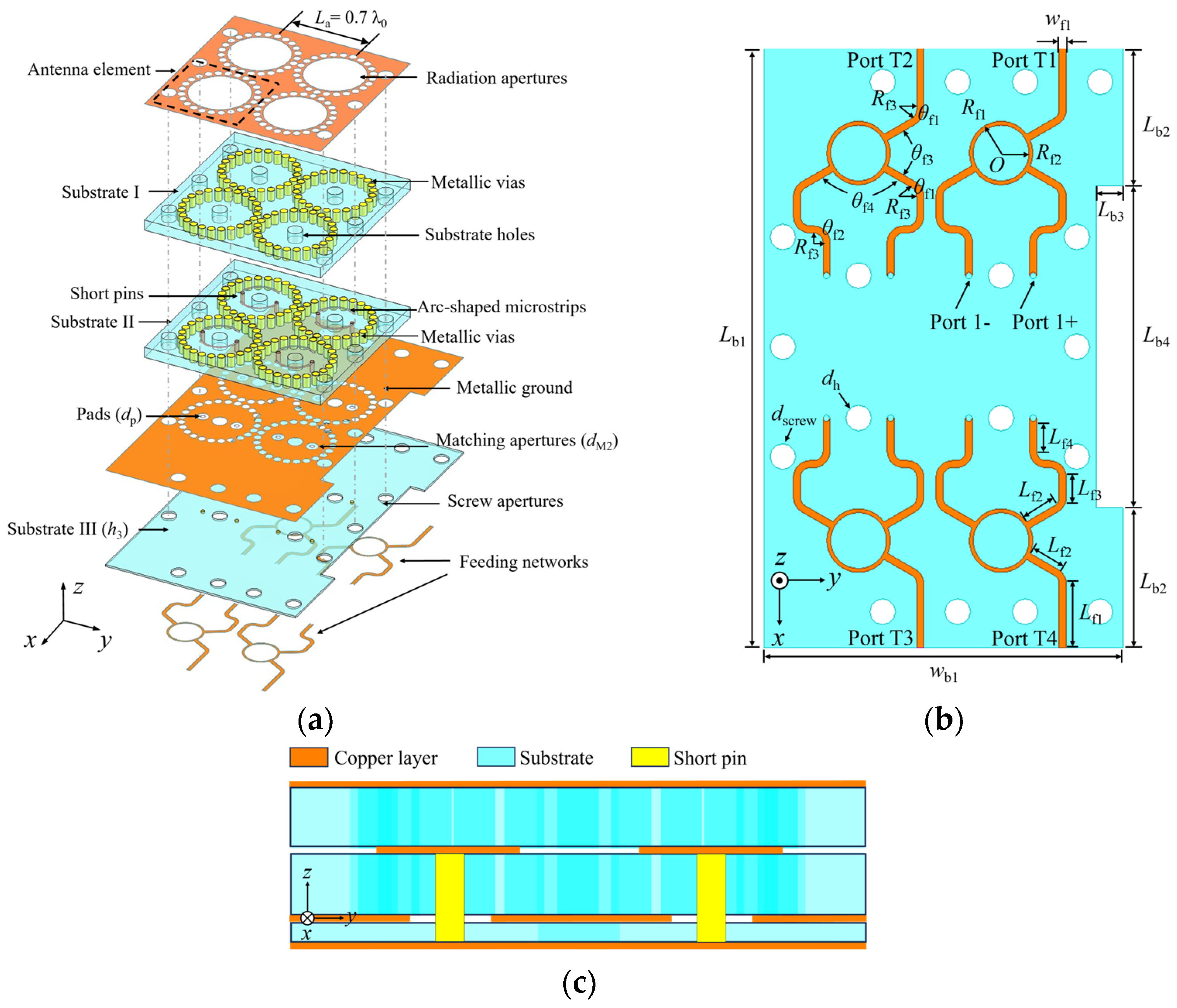
3. Antenna Array
3.1. Configuration of the Antenna Array
3.2. Differential Feeding Networks
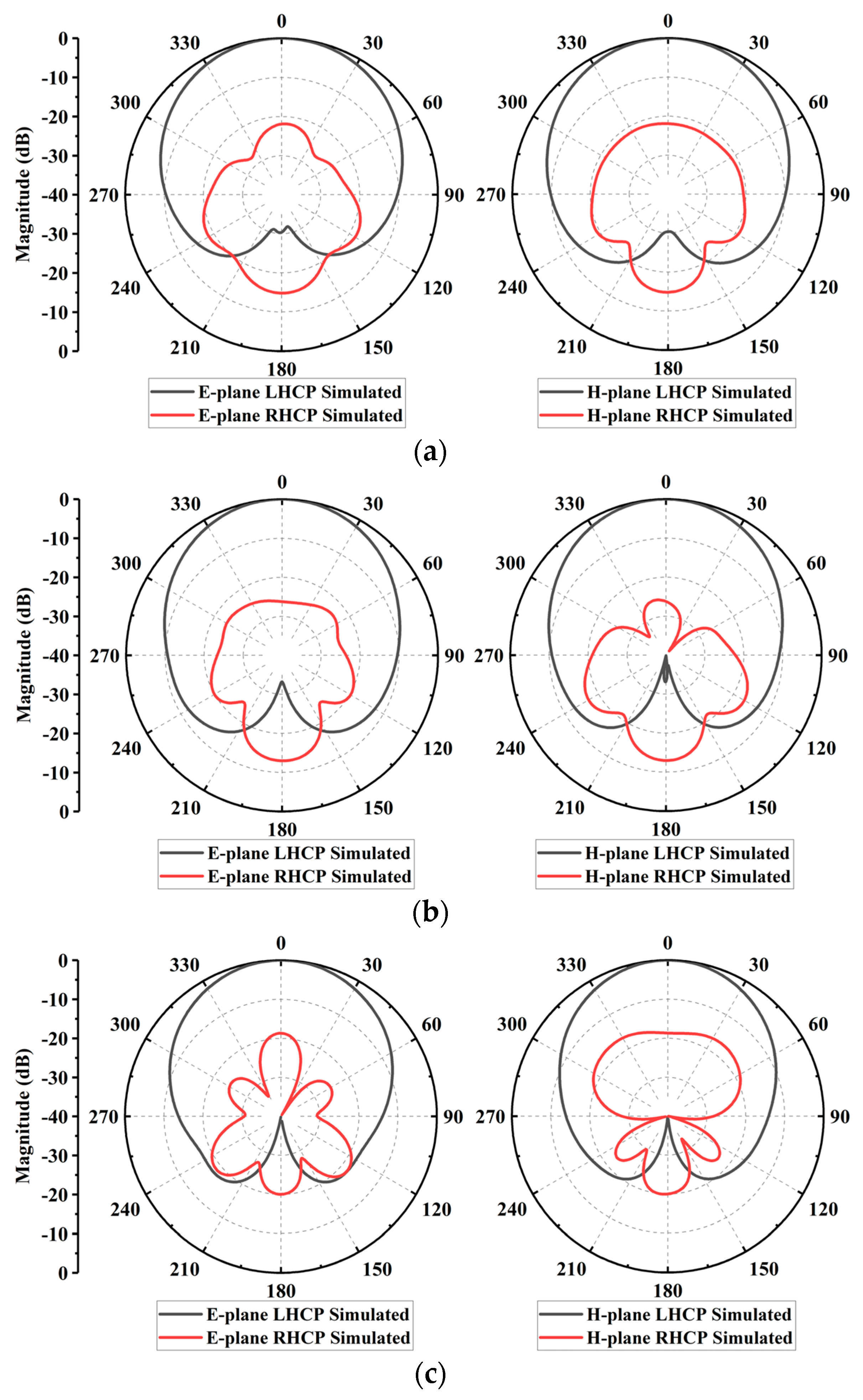
4. Experiments and Discussion
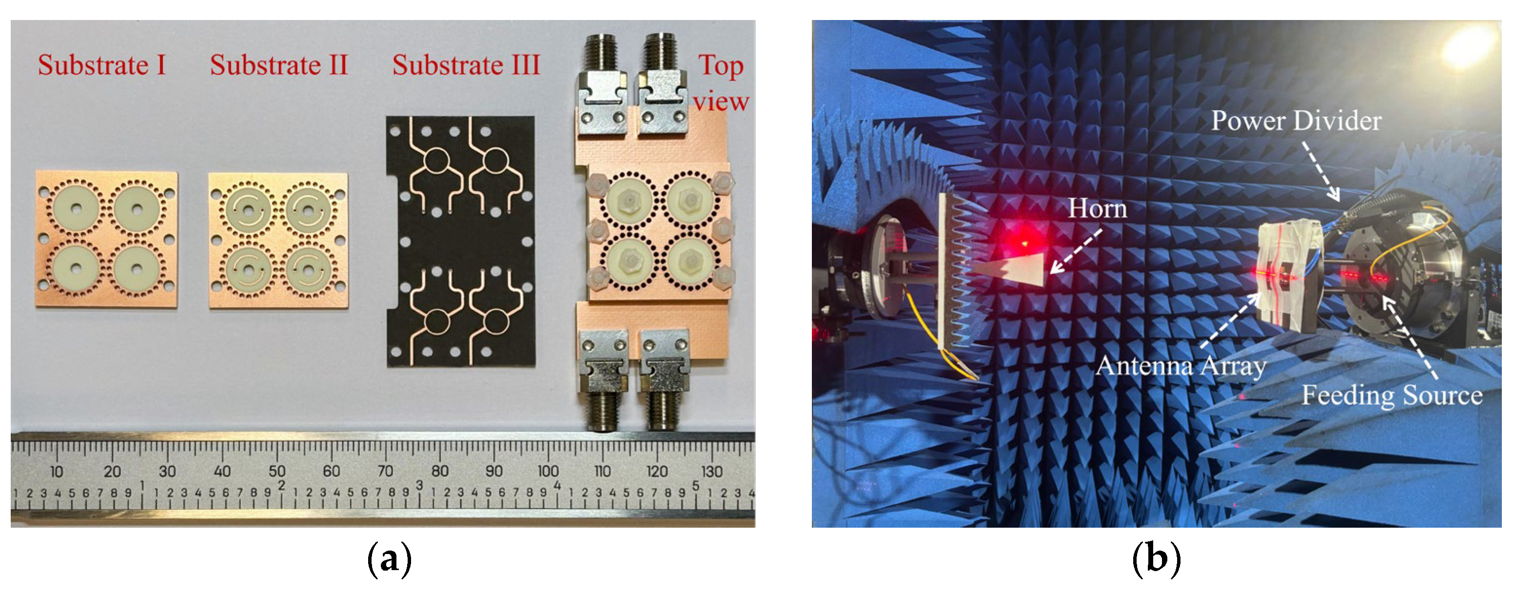
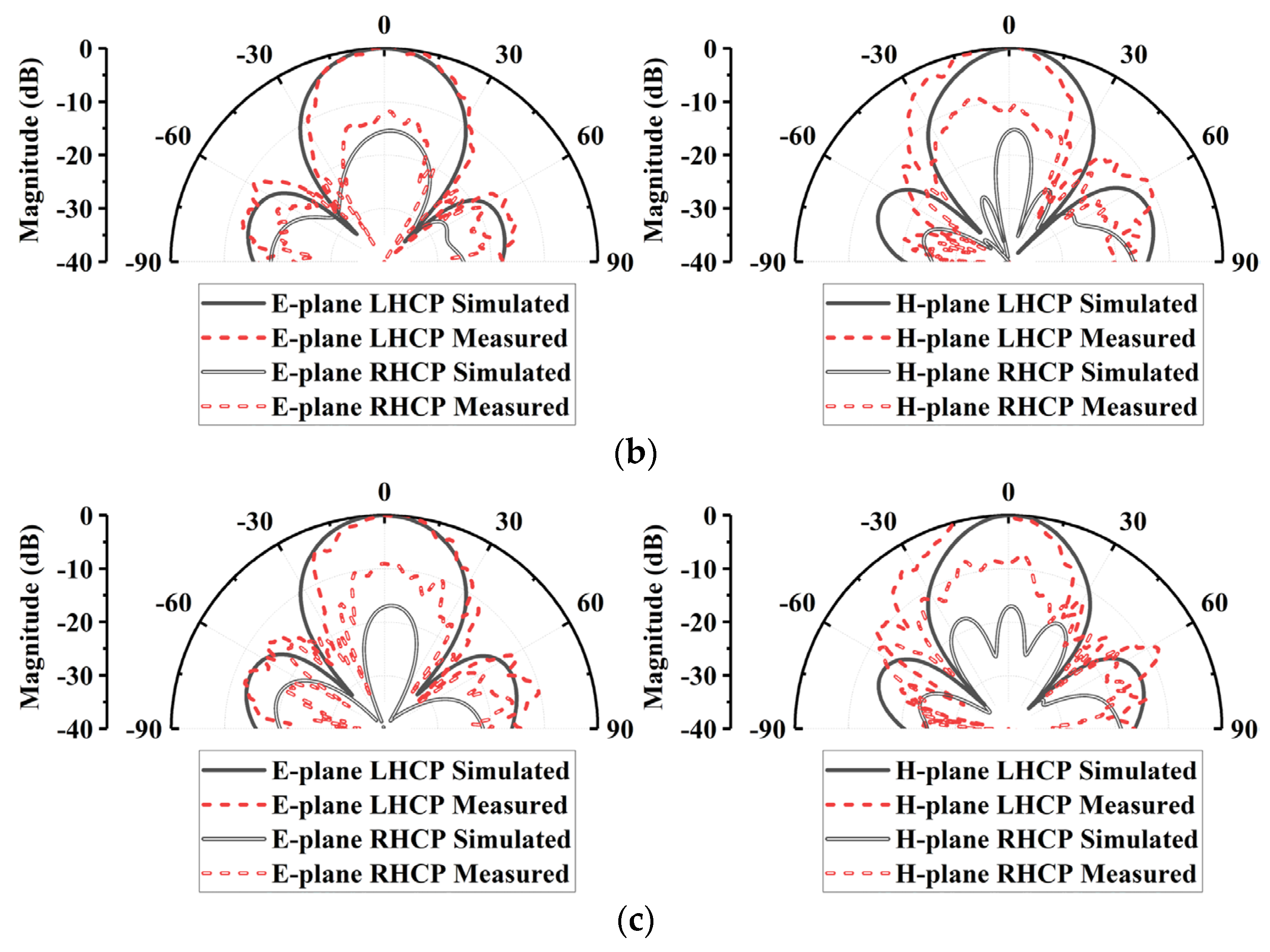
4.1. Prototype and Measurements
4.2. Inaccuracy Analysis
4.3. Comparison and Discussion
5. Conclusions
Author Contributions
Funding
Data Availability Statement
Acknowledgments
Conflicts of Interest
Abbreviations
| CP | Circularly polarized |
| SIW | Substrate-integrated waveguide |
| AR | Axial ratio |
| LP | linear polarized |
| LHCP | Left-handed circularly polarized |
| RHCP | Right-handed circularly polarized |
| Imp. BW | Impendence bandwidth |
| Cross-Pol. | Cross polarization |
| SAR | Synthetic aperture radar |
| IoT | Internet of Things |
| EMC | Electromagnetic compatibility |
References
- Zhu, J.; Liao, S.; Yang, Y.; Li, S.; Xue, Q. 60 GHz Dual-Circularly Polarized Planar Aperture Antenna and Array. IEEE Trans. Antennas Propag. 2018, 66, 1014–1019. [Google Scholar] [CrossRef]
- Albakosh, W.; Asfour, R.; Khalil, Y.; Khamas, S.K. Wideband Millimeter-Wave Perforated Hemispherical Dielectric Resonator Antenna. Electronics 2024, 13, 1694. [Google Scholar] [CrossRef]
- Hirokawa, J.; Arai, H.; Goto, N. Cavity-Backed Wide Slot Antenna. IEE Proc. H (Microw. Antennas Propag.) 1989, 136, 29–33. [Google Scholar] [CrossRef]
- Ruan, X.; Qu, S.-W.; Zhu, Q.; Ng, K.B.; Chan, C.H. A Complementary Circularly Polarized Antenna for 60-GHz Applications. IEEE Antennas Wirel. Propag. Lett. 2017, 16, 1373–1376. [Google Scholar] [CrossRef]
- Paryani, R.C.; Wahid, P.F.; Behdad, N. A Wideband, Dual-Polarized, Substrate-Integrated Cavity-Backed Slot Antenna. IEEE Antennas Wirel. Propag. Lett. 2010, 9, 645–648. [Google Scholar] [CrossRef]
- Deng, Q.J.; Pan, Y.M.; Liu, X.Y.; Leung, K.W. A Singly-Fed Dual-Band Aperture-Sharing SIW Cavity-Backed Slot Antenna with Large Frequency Ratio. IEEE Trans. Antennas Propag. 2023, 71, 1971–1976. [Google Scholar] [CrossRef]
- Wang, S.; Wan, C.; Chung, K.L.; Zheng, Y. Investigation of Compact Near-Equidistant Multimode Resonator Integrating Skyrmionic Metamaterial with SIW Cavity and Its Application in Dielectric Material Detection. IEEE Trans. Microw. Theory Tech. 2024, 1–16. [Google Scholar] [CrossRef]
- Zhang, L.; Wu, K.; Wong, S.-W.; He, Y.; Chu, P.; Li, W.; Wang, K.X.; Gao, S. Wideband High-Efficiency Circularly Polarized SIW-Fed S-Dipole Array for Millimeter-Wave Applications. IEEE Trans. Antennas Propag. 2020, 68, 2422–2427. [Google Scholar] [CrossRef]
- Wu, Q.; Yin, J.; Yu, C.; Wang, H.; Hong, W. Low-Profile Millimeter-Wave SIW Cavity-Backed Dual-Band Circularly Polarized Antenna. IEEE Trans. Antennas Propag. 2017, 65, 7310–7315. [Google Scholar] [CrossRef]
- Wang, X.-C.; Xia, Y.-J.; Yang, J.-H.; Lu, W.-Z. Wideband High-Gain Circularly Polarized Substrate Integrated Cavity Antenna Array for Millimeter-Wave Applications. IEEE Trans. Antennas Propag. 2023, 71, 1041–1046. [Google Scholar] [CrossRef]
- Yan, Y.-D.; Jiao, Y.-C.; Cheng, H.-T.; Zhang, C. A Low-Profile Dual-Circularly Polarized Wide-Axial-Ratio-Beamwidth Slot Patch Antenna with Six-Port Feeding Network. IEEE Antennas Wirel. Propag. Lett. 2021, 20, 2486–2490. [Google Scholar] [CrossRef]
- Ji, Z.; Sun, G.-H.; Wong, H. A Wideband Circularly Polarized Complementary Antenna for Millimeter-Wave Applications. IEEE Trans. Antennas Propag. 2022, 70, 2392–2400. [Google Scholar] [CrossRef]
- Wu, Q.; Wang, H.; Yu, C.; Hong, W. Low-Profile Circularly Polarized Cavity-Backed Antennas Using SIW Techniques. IEEE Trans. Antennas Propag. 2016, 64, 2832–2839. [Google Scholar] [CrossRef]
- Guan, D.-F.; Ding, C.; Qian, Z.-P.; Zhang, Y.-S.; Jay Guo, Y.; Gong, K. Broadband High-Gain SIW Cavity-Backed Circular-Polarized Array Antenna. IEEE Trans. Antennas Propag. 2016, 64, 1493–1497. [Google Scholar] [CrossRef]
- Li, Y.; Luk, K.-M. A 60-GHz Wideband Circularly Polarized Aperture-Coupled Magneto-Electric Dipole Antenna Array. IEEE Trans. Antennas Propag. 2016, 64, 1325–1333. [Google Scholar] [CrossRef]
- Wang, W.; Jin, H.; Yu, W.; Zhang, X.H.; Chin, K.-S.; Luo, G.Q. A Wideband Circularly Polarized 2 × 2 Filtenna Array With Multiple Radiation Nulls. IEEE Antennas Wirel. Propag. Lett. 2022, 21, 595–599. [Google Scholar] [CrossRef]
- Hao, Z.-C.; Liu, X.; Huo, X.; Fan, K. Planar High-Gain Circularly Polarized Element Antenna for Array Applications. IEEE Trans. Antennas Propag. 2015, 63, 1937–1948. [Google Scholar] [CrossRef]
- Zhang, Z.Y.; Guo, Y.X.; Ong, L.C.; Chia, M.Y.W. A New Wide-Band Planar Balun on a Single-Layer PCB. IEEE Microw. Wirel. Compon. Lett. 2005, 15, 416–418. [Google Scholar] [CrossRef]
- Srivastava, G.; Mohan, A. A Differential Dual-Polarized SIW Cavity-Backed Slot Antenna. IEEE Trans. Antennas Propag. 2019, 67, 3450–3454. [Google Scholar] [CrossRef]
- Hou, Y.; Zhang, Y.; Mao, J. A Wideband Polarization Grid Loaded Circularly Polarized Laminated Resonator Antenna. In Proceedings of the 2021 15th European Conference on Antennas and Propagation (EuCAP), Dusseldorf, Germany, 22–26 March 2021; pp. 1–4. [Google Scholar]
- Hou, Y.; Zhang, Y.; Mao, J. A Differential Wideband Circularly Polarized Laminated Resonator Antenna. IEEE Antennas Wirel. Propag. Lett. 2023, 22, 278–282. [Google Scholar] [CrossRef]
- Kulkarni, P.B. Wideband Circularly Polarized SIW Cavity-backed Slot Antenna with Sequential Rotation Feeding. Microw. Opt. Technol. Lett. 2016, 58, 2566–2570. [Google Scholar] [CrossRef]
- Zhu, J.; Li, S.; Liao, S.; Yang, Y.; Zhu, H. 60 GHz Substrate-Integrated-Waveguide-Fed Patch Antenna Array With Quadri-Polarization. IEEE Trans. Antennas Propag. 2018, 66, 7406–7411. [Google Scholar] [CrossRef]
- Guo, Q.-Y.; Yi, X.; Lv, R.C.; He, W.; Yang, C.F.; Shu, G.; Tian, Y.; Wong, H. A High-Gain, Wideband, Circularly Polarized Antenna With Multibeam Radiation for Millimeter-Wave Applications. IEEE Trans. Antennas Propag. 2024, 72, 1373–1384. [Google Scholar] [CrossRef]
- Hou, Y.; Shao, Z.; Zhang, Y.; Mao, J. A Wideband Differentially Fed Dual-Polarized Laminated Resonator Antenna. IEEE Trans. Antennas Propag. 2021, 69, 4148–4153. [Google Scholar] [CrossRef]
- Tong, C.-W.; Tang, H.; Qin, W.; Yang, W.-W.; Zhang, X.-F.; Chen, J.-X. Differentially Inserted-Fed Compact Dual-Band Circularly Polarized Dielectric Resonator Antenna. IEEE Antennas Wirel. Propag. Lett. 2019, 18, 2498–2502. [Google Scholar] [CrossRef]
- Snyder, A.S.; Love, J.D. Optical Waveguide Theory; Chapman and Hall: London, UK, 1983; pp. 374–399. [Google Scholar]
- Mitha, T.; Pour, M. Principles of Adaptive Element Spacing in Linear Array Antennas. Sci. Rep. 2021, 11, 5584. [Google Scholar] [CrossRef]
- Aliakbari, H.; Mosalanejad, M.; Soens, C.; Vandenbosch, G.A.E.; Lau, B.K. Wideband SIW-Based Low-Cost Multilayer Slot Antenna Array for E-Band Applications. IEEE Trans. Compon. Packag. Technol. 2019, 9, 1568–1575. [Google Scholar] [CrossRef]


| Parameter | D1 | C1 | h1 | h2 | l1 | w1 | p |
| Value | 14 | 10 | 1.524 | 1.524 | 6.47 | 0.3 | 1.53 |
| Parameter | d | d1 | dR | dh | ds | dM | - |
| Value | 1 | 5 | 4.2 | 1 | 0.5 | 1.1 | - |
| Ref. | Feeding Method | Center Frequency (GHz) | −10 dB Imp. BW (%) | 3 dB AR. BW (%) | 3 dB Gain BW (%) | Overlaid BW (%) | Size () | Cross-Pol. (dB) | Peak Gain (dBi/dBic) |
|---|---|---|---|---|---|---|---|---|---|
| [8] | Single | 30 | 43 | 36.1 | 38 (1 dB) | 36.1 | 1.0 × 1.0 × 0.315 | <−15 * | 7.5 |
| [9] | Single | 37.5; 47.8 | 1.1; 1.4 | 1.1; 1.5 | n.a. | n.a. | n.a. × 1.27 × 0.081 | <−15 * | 5.7 |
| [10] | Single | 29.17 | 24.37 | 26.14 | 33.85 | 20.36 | 0.83 × 0.83 × 0.20 | n.a. | 10.53 |
| [20] | Diff | 5.09 | 30.27 | 26.16 | >30.27 | 26.16 | 0.53 × 0.53 × 0.389 | <−10 * | 9.82 |
| [21] | Diff | 5.0 | 65.91 | 64 | 52 | 52 | 1.33 × 1.33 × 0.115 | <−20 * | 6.97 |
| [22] | Diff | 10.5 | >34 | n.a. | n.a. | n.a. | 0.53 × 0.53 × 0.137 | <−10 * | 6.0 |
| This work | Diff | 19.0 | 34.4 | 20.6 | 39.9 | 20.6 | 0.89 × 0.89 × 0.19 | −25 | 8.14 |
| Parameter | h1 | h2 | h3 | dp | dM2 | dh | dscrew |
| Value (mm) | 1.524 | 1.524 | 0.254 | 0.7 | 1.6 | 1.0 | 2.0 |
| Parameter | wf1 | wb1 | La | Lb1 | Lb2 | Lb3 | Lb4 |
| Value (mm) | 0.54 | 28.0 | 11.1 | 46.888 | 10.894 | 2.1 | 25.1 |
| Parameter | Lf1 | Lf2 | Lf3 | Lf4 | Rf1 | Rf2 | Rf3 |
| Value (mm) | 5.0 | 2.3 | 1.61 | 2.59 | 2.47 | 2.18 | 1.0 |
| Parameter | θf1 | θf2 | θf3 | θf4 | - | - | - |
| Value (deg) | 60 | 90 | 60 | 120 | - | - | - |
| Ref. | Feeding Method | Center Frequency (GHz) | −10 dB Imp. BW (%) | 3 dB AR. BW (%) | 3 dB Gain BW (%) | Overlaid BW (%) | Size () | Peak Gain (dBic/dBi) |
|---|---|---|---|---|---|---|---|---|
| [8] | Single | 30 | 27.6 | 32.7 | 30 | 27.6 | 5.90 × 5.90 × 0.4725 | 25.2 |
| [10] | Single | 29 | 21.94 | 22.07 | 29.03 | 21.72 | 6.68 × 6.68 × 0.27 | 26.1 |
| [13] | Single | 10 | 21 | 18 | 9.3 | n.a. | 3.70 × 3.70 × 0.11 | 13.2 |
| [14] | Single | 20 | 15.9 | 13.8 | >15.9 | 13.8 | 12 × 12.67 × 0.13 | 25.9 |
| [15] | Single | 61 | 18.2 | 16.4 | >18.2 | 16.4 | 6.22 × 6.92 × 0.50 | 26.1 |
| [17] | Single | 6.6175 | 3.17 | 0.98 | >0.98 | 0.98 | 3.69 × 3.69 × 0.035 | 20.1 |
| [23] | Diff | 60.5 | 11.6 | >9.8 | >11.6 | >9.8 | n.a. × n.a. × 0.45 | 12.2 |
| This work | Diff | 19.0 | 32.6 | 13.8 | 41.8 | 13.8 | 2.98 × 1.78 × 0.21 | 10.6 |
Disclaimer/Publisher’s Note: The statements, opinions and data contained in all publications are solely those of the individual author(s) and contributor(s) and not of MDPI and/or the editor(s). MDPI and/or the editor(s) disclaim responsibility for any injury to people or property resulting from any ideas, methods, instructions or products referred to in the content. |
© 2025 by the authors. Licensee MDPI, Basel, Switzerland. This article is an open access article distributed under the terms and conditions of the Creative Commons Attribution (CC BY) license (https://creativecommons.org/licenses/by/4.0/).
Share and Cite
Wang, C.; Li, X.-C.; Keezer, D. Differential-Fed Wideband Circularly Polarized SIW Cavity-Backed Slot Antenna Array. Electronics 2025, 14, 2389. https://doi.org/10.3390/electronics14122389
Wang C, Li X-C, Keezer D. Differential-Fed Wideband Circularly Polarized SIW Cavity-Backed Slot Antenna Array. Electronics. 2025; 14(12):2389. https://doi.org/10.3390/electronics14122389
Chicago/Turabian StyleWang, Chao, Xiao-Chun Li, and David Keezer. 2025. "Differential-Fed Wideband Circularly Polarized SIW Cavity-Backed Slot Antenna Array" Electronics 14, no. 12: 2389. https://doi.org/10.3390/electronics14122389
APA StyleWang, C., Li, X.-C., & Keezer, D. (2025). Differential-Fed Wideband Circularly Polarized SIW Cavity-Backed Slot Antenna Array. Electronics, 14(12), 2389. https://doi.org/10.3390/electronics14122389