Article

Optimized Submodule Capacitor Ripple Voltage Suppression of an MMC-Based Power Electronic Transformer

by
Jinmu Lai
1,*,
Zijian Wu
1,
Xianyi Jia
1,
Yaoqiang Wang
1,
Yongxiang Liu
2 and
Xinbing Zhu
2
1
The School of Electrical and Information Engineering, Zhengzhou University, Zhengzhou 450001, China
2
Xuchang Intelligent Building, Xuchang Intelligent Relay Co., Ltd., Xuchang 461111, China
*
Author to whom correspondence should be addressed.
Electronics 2025, 14(12), 2385; https://doi.org/10.3390/electronics14122385
Submission received: 14 April 2025 / Revised: 30 May 2025 / Accepted: 3 June 2025 / Published: 11 June 2025

Abstract

:
Modular multilevel converter (MMC)-based power electronic transformers (PETs) present a promising solution for connecting AC/DC microgrids to facilitate renewable energy access. However, the capacitor ripple voltage in MMC-based PET submodules hinders volume optimization and power density enhancement, significantly limiting their application in distribution networks. To address this issue, this study introduces an optimized method for suppressing the submodule capacitor ripple voltage in MMC-based PET systems under normal and grid fault conditions. First, an MMC–PET topology featuring upper and lower arm coupling is proposed. Subsequently, a double-frequency circulating current injection strategy is incorporated on the MMC side to eliminate the double-frequency ripple voltage of the submodule capacitor. Furthermore, a phase-shifting control strategy is applied in the isolation stage of the dual-active bridge (DAB) to transfer the submodule capacitor selective ripple voltages to the isolation stage coupling link, effectively eliminating the fundamental frequency ripple voltage. The optimized approach successfully suppresses capacitor ripples without increasing current stress on the isolated-stage DAB switches, even under grid fault conditions, which are not addressed by existing ripple suppression methods, thereby reducing device size and cost while ensuring reliable operation. Specifically, the peak-to-peak submodule capacitor ripple voltage is reduced from 232 V to 10 V, and the peak current of the isolation-stage secondary-side switch is limited to ±90 A. The second harmonic ripple voltage on the LVDC bus can be decreased from ±5 V to ±1 V with the proposed method under the asymmetric grid voltage condition. Subsequently, a system simulation model is developed in MATLAB/Simulink. The simulation results validated the accuracy of the theoretical analysis and demonstrated the effectiveness of the proposed method.

1. Introduction

With the increasing integration of renewable energy sources and the rising prevalence of electric vehicles, energy storage units, and uncontrollable loads, diversified power supply systems centered around distributed generation present new challenges to conventional grid infrastructure. The conventional top-down distribution system relying on traditional transformers cannot satisfy these evolving requirements. Transitioning to a multivoltage level AC/DC hybrid distribution network architecture can significantly enhance the simplicity of the system structure and flexibility of equipment integration. The power electronic transformer (PET), also called a solid state transformer or energy router, represents a category of power electronic devices that link medium and low voltage systems through high-frequency transformers (HFTs). Owing to its adaptability in accommodating renewable energy sources and its precise control over power flow, port voltage, and current, the PET is a potential solution for AC/DC hybrid distribution grids. A typical DC distribution network architecture based on a PET is illustrated in Figure 1 [1,2].
The three-stage PET exhibits excellent controllability, flexibility, and technological maturity, making it a subject of extensive research and practical application. Based on the connection form with the medium voltage alternating current (MVAC) port, the PET can be divided into a cascaded H-bridge (CHB)-based PET, modular multilevel converter-based PET (MMC–PET), and neutral point clamped (NPC) technology-based PET. Nevertheless, the absence of a medium voltage direct current (MVDC) port in CHB-based PET configurations restricts their utilization within smart grid systems [3,4]. Both the NPC-based PET and MMC-PET can offer four output ports. However, as the AC voltage level increases, the NPC converter tends to exhibit a subpar modular performance. In contrast, the MMC technology is extensively employed in the input stage of the PET system owing to its modular design, high scalability, low harmonics, and reduced switching losses [5]. The phase-shifted DAB converter is applied to the intermediate isolation stage because of its simple control method [6], while the three-phase full-bridge inverter is applied to the output stage. A typical PET topology is shown in Figure 2. The low voltage direct current (LVDC) port can be connected to distributed renewable energy systems, energy storage systems, and DC loads. The MVDC port can achieve DC distribution, which provides a promising solution for large-scale renewable energy grid connections. Therefore, the multiple output ports provided by the PET (MVAC, MVDC, LVDC, and LVAC) are indispensable in new energy distribution systems [7].
The constant voltage value of the submodule capacitor in the MMC is a prerequisite for the stable operation of the PET. The MMC arm current generates a low-frequency ripple on the submodule capacitor through switching devices. To solve this problem, the DAB unit found in the later stage of the MMC submodule can be used to transfer the ripple power flowing into the submodule capacitor to the low voltage side through the power control of the DAB, such that all submodule ripple power can be coupled and offset, thus achieving full suppression of the low-frequency capacitor voltage ripple [8]. However, this method will cause a corresponding ripple in the high-frequency current amplitude of the isolation stage DAB converter, and an excessive ripple will increase the conduction loss and current stress on the switching devices in the isolation stage [8]. Reference [9] proposed a voltage closed-loop ripple control scheme for the MMC–PET based on ripple power transmission. In this method, a voltage closed-loop decoupling control structure is constructed under dual rotating coordinates, effectively suppressing fundamental and second harmonic capacitor ripples. Simultaneously, an optimal partial ripple power transmission-based operating strategy that optimizes the current stress of the DAB is proposed. Optimizing the modulation strategy of DAB converters can also reduce current stress. Reference [10] proposed an extended phase shift (EPS) control strategy integrated with coupled inductors, which eliminates backflow power (BFP) by decoupling the direct power transfer (DPT) path and dynamically adjusting current slopes. This approach extends the zero-voltage switching (ZVS) range to light-load conditions while reducing conduction losses and current stress, thereby enhancing efficiency in bidirectional converters with wide voltage variations. Reference [11] proposed a peak current feedforward control to accelerate dynamic response in phase-shifted full-bridge converters, while [12] optimized triple phase shift modulation to minimize transformer losses via harmonic suppression, collectively advancing high-efficiency power conversion under variable operating conditions.
In addition, injecting a zero-sequence voltage or current can also effectively suppress the ripple voltage of submodules. Reference [13] proposed a zero-sequence voltage injection control strategy, which reduces the current stress of the isolation stage switching device by injecting a zero-sequence voltage into the cascaded H-bridge converter on the AC side. Reference [14] proposed circulating current injection methods based on open-loop estimation and closed-loop control for reducing the double-frequency ripple voltage in a capacitor. However, this method did not eliminate the fundamental frequency ripple occupying a larger proportion in the capacitor nor optimize the current stress of the MMC arm. Reference [15] proposed injecting a suitable amplitude and phase of the third-order common-mode voltage with the second circulating current, and selecting an optimal modulation ratio, such that the ripple capacitor voltage in the objective function and the capacitance value can be minimized under a certain fluctuation rate of capacitor voltage. However, further improvements are required when this method is applied to multiport PETs.
In this study, a modified MMC–PET topology with interstage high-frequency coupling (ISHFC) was designed, and a coordinated ripple suppression strategy combining partial ripple voltage suppression (PRVS) in the MMC stage and selective ripple voltage suppression (SRVS) in the DAB stage was proposed to eliminate the submodule capacitor voltage ripple and the LVDC bus voltage ripple considering asymmetric grid voltage operation conditions. The contributions of this paper are summarized as follows:
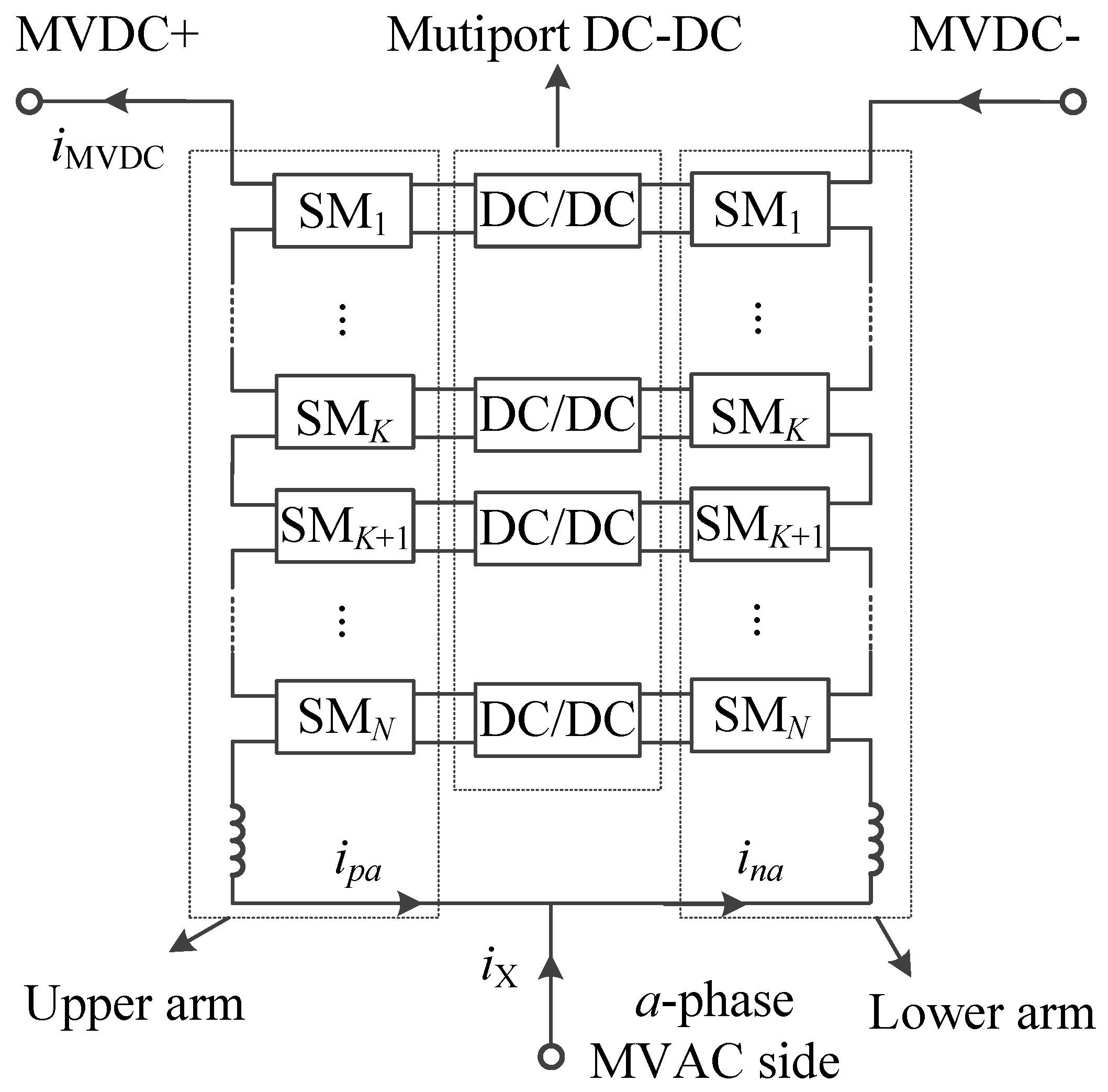
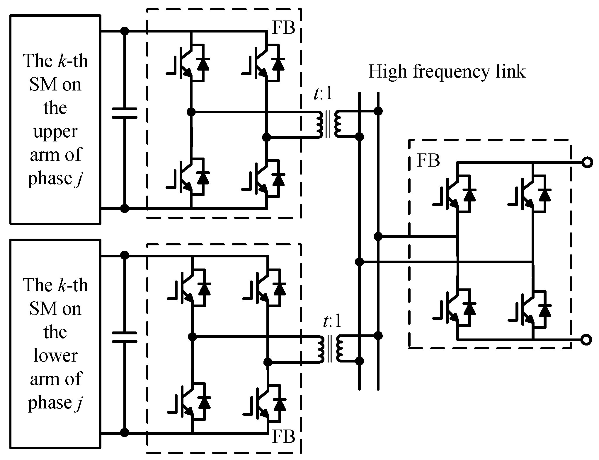
  • This article proposes an MMC-type PET topology with high-frequency coupling of upper and lower arms in the isolation stage, which reduces the number of full-bridge modules and makes the structure more compact.
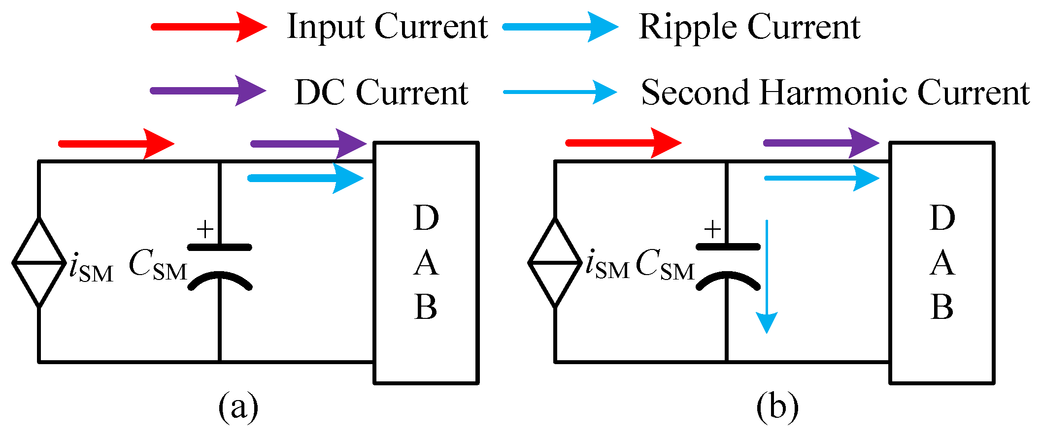
  • The submodule capacitor ripple voltage coupling characteristics of the modified MMC-PET were analyzed considering symmetry and asymmetry grid voltage conditions. It is found that, under the asymmetry grid voltage condition, an unbalanced second-order ripple current can flow into the LVDC with the fully ripple voltage suppression in the DAB stage, causing a certain ripple in the LVDC side voltage.
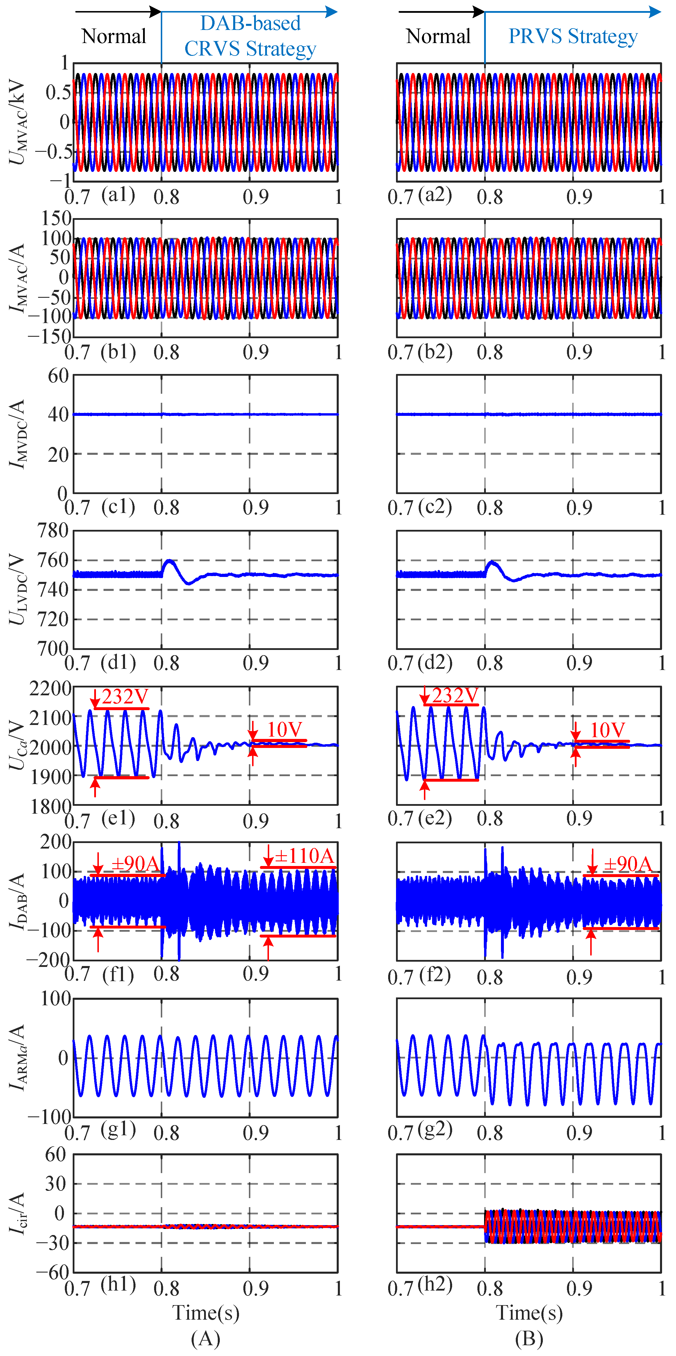
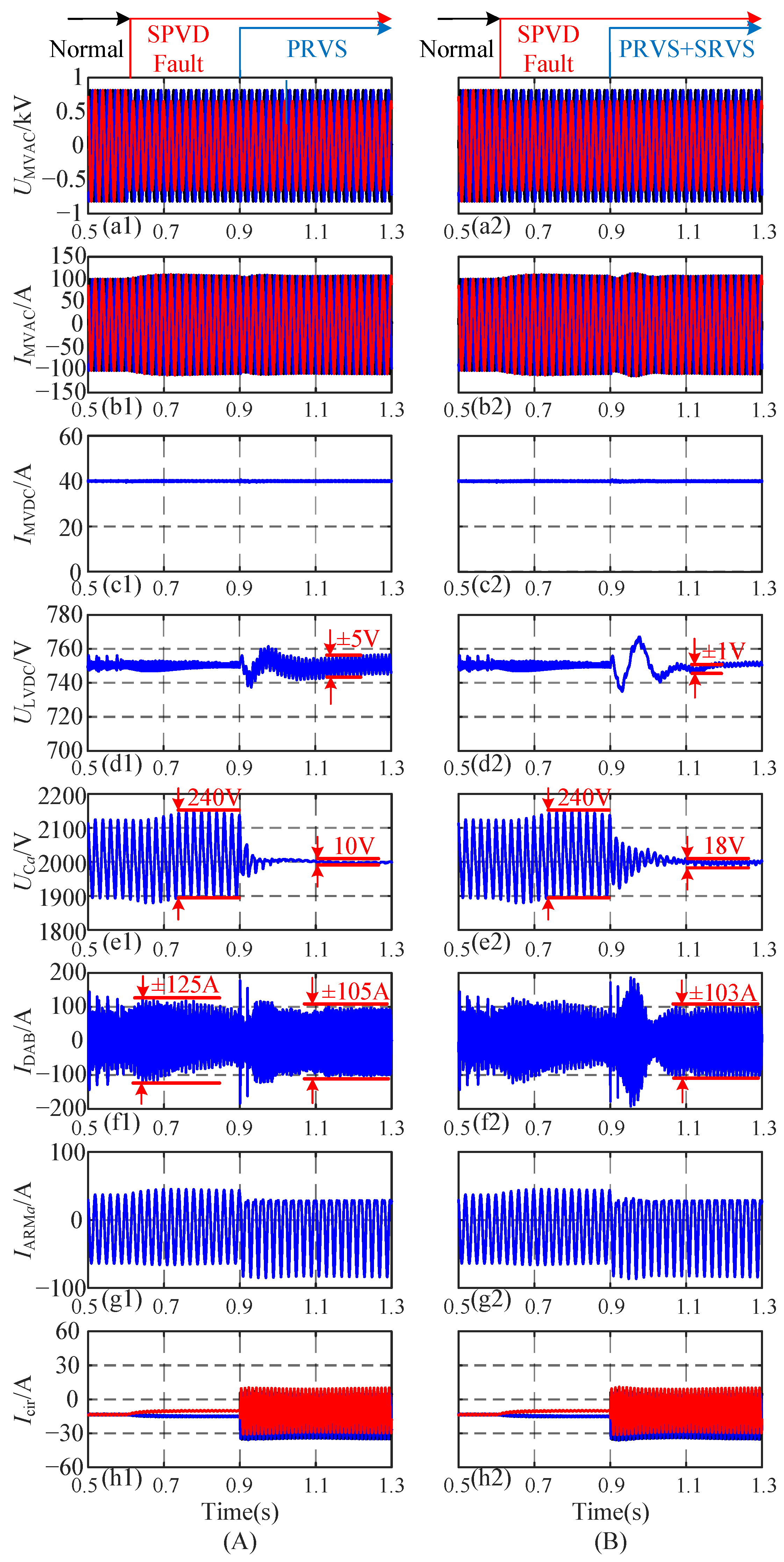
  • A coordinated ripple suppression strategy combining PRVS in the MMC stage and SRVS in the DAB stage was designed to eliminate both the submodule capacitor voltage ripple and the LVDC bus voltage ripple considering asymmetric grid voltage operation conditions. The proposed PRVS + SRVS strategy can effectively suppress both the fundamental and second-order harmonic components of the submodule capacitor ripple voltage without increasing the current stress on the isolation-stage DAB switches. The simulation results showed that the peak-to-peak submodule capacitor ripple voltage was reduced from 232 V to 10 V, while the peak current of the isolation stage secondary side (ISSS) switch was limited to ±90 A. The second harmonic ripple voltage on the LVDC bus can be decreased from ±5 V to ±1 V with the proposed SRVS method under the asymmetric grid voltage condition.
  • The improved phase shift modulation strategy of PRVS for the DAB stage was designed based on a proportional repetitive controller, which enables real-time multi-frequency ripple suppression and successfully transfers ripple power to the LVDC bus, significantly improving voltage quality. Under both normal and asymmetric grid conditions, the method ensured stable operation of the LVDC side with minimal ripple.
The rest of the paper is organized as follows: First, this study proposes an MMC–PET topology with upper and lower arm coupling. Then, based on the ripple power transfer strategy, the coupling characteristics of the submodule ripple power under symmetrical and asymmetrical grid side voltages of this topology are analyzed. Next, an MMC-based PRVS method coordinated with the DAB-based SRVS method is proposed. Finally, the simulation results are verified.

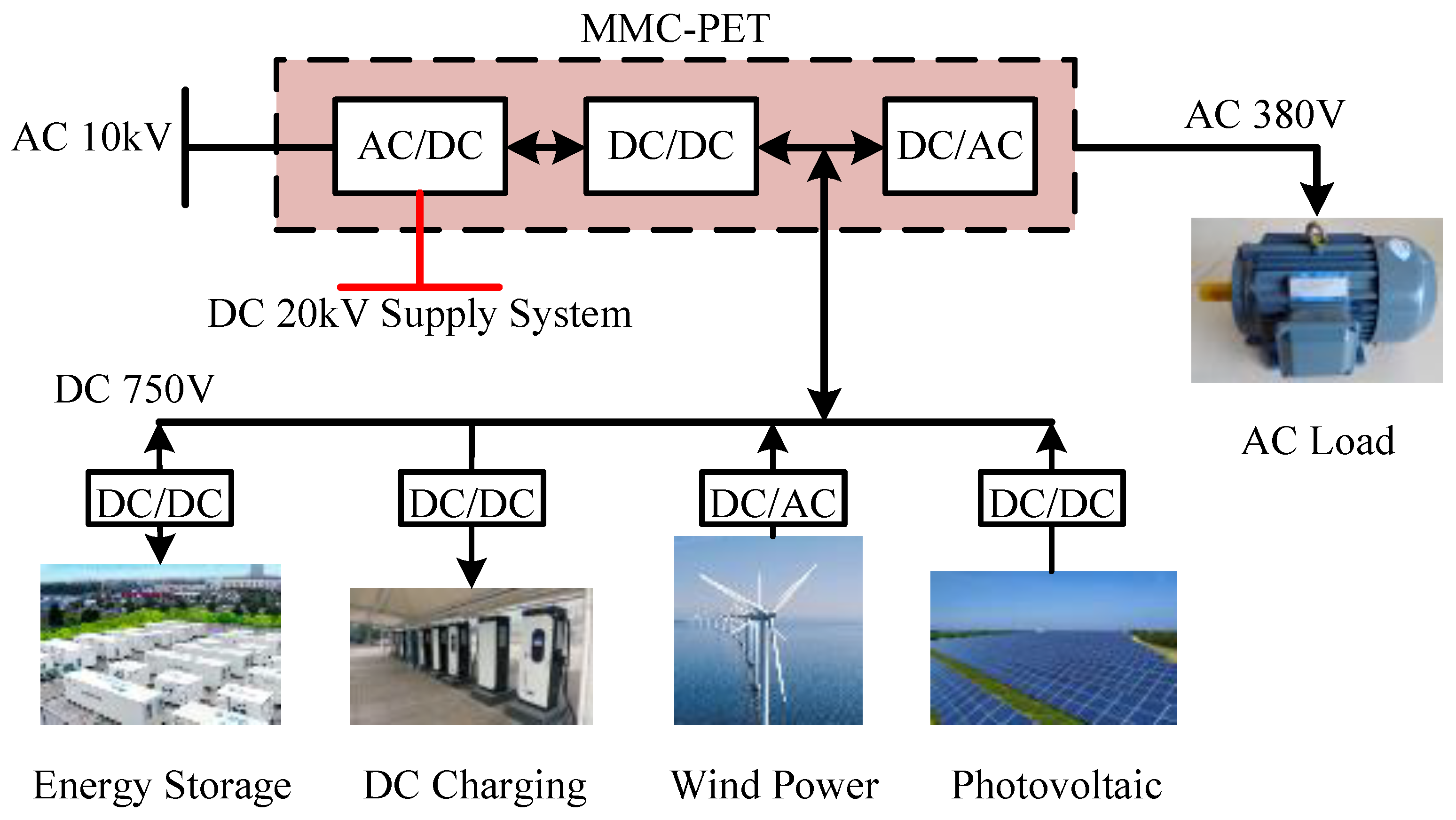
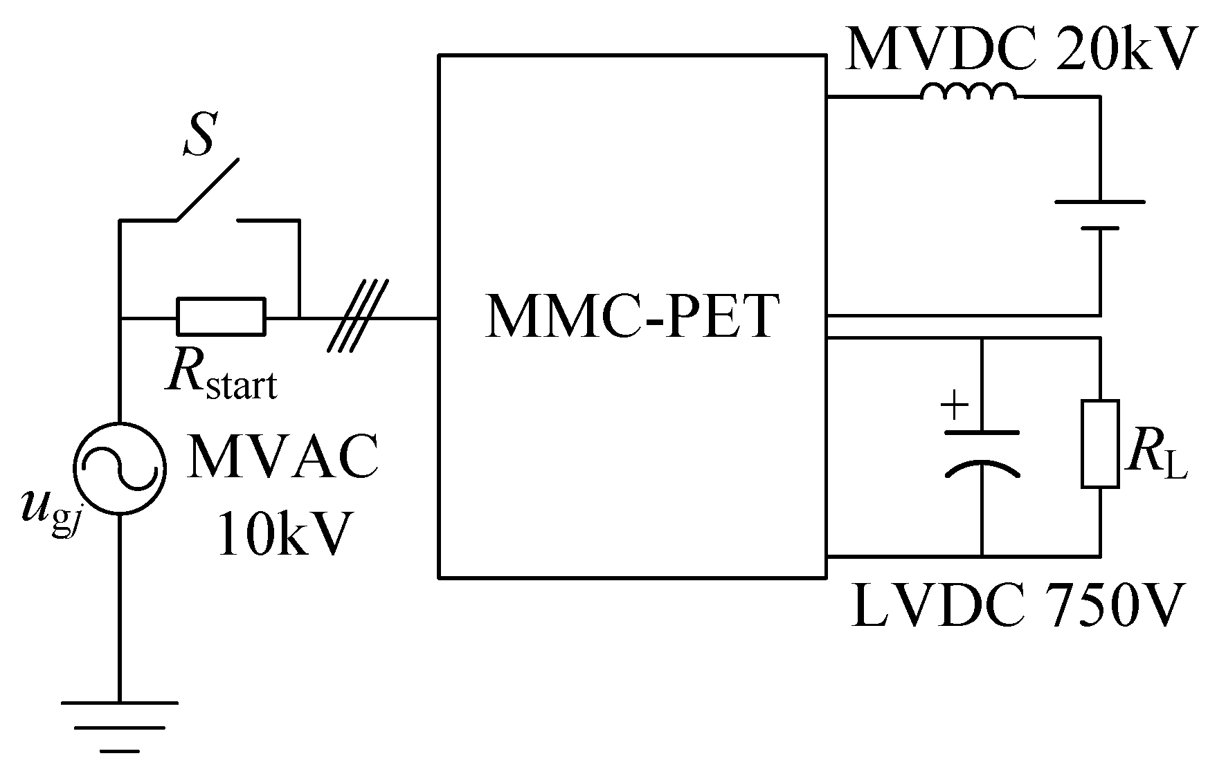
2. Topology and Coupling Characteristic Analysis of the MMC-Type PETs with Upper and Lower Arm Coupling

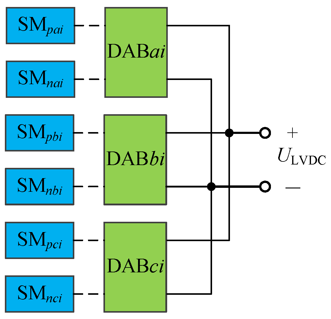
2.1. MMC–PET Topology

Based on the topology illustrated in Figure 1, this study proposes an MMC-type multiport PET topology employing isolation stage high-frequency coupling (ISHFC) between the upper and lower arms. This topology restricts a high-frequency interconnection to the corresponding submodules of the same phase in the upper and lower arms, which not only solves the problem of excessive capacitor volume in MMC submodules, but also reduces the number of full-bridge modules. The schematic diagram of its structure is shown in Figure 3, where i MVDC denotes the MVDC bus current, i p a denotes the upper arm current of phase a, and i n a denotes the lower arm current of phase a. i X is the grid side current.
The MMC-type multiport PET topology with the ISHFC of upper and lower arms includes an MMC and several multiport DC–DC converters. The MMC consists of three phases with the same input structure. Each phase of the MMC includes one upper arm, one lower arm, and two arm inductors. Each arm comprises N series-connected full-bridge modules, designated as 1,..., N. The multiport DC–DC converter consists of three power modules and two dual-winding HFTs. There are N multiport DC–DC converters per phase in the MMC. To couple and cancel the fundamental frequency ripple power of the submodule capacitors in an MMC, the DC side of the full-bridge module connected on the primary side of the dual-winding transformer in the k-th multiport DC–DC converter is connected to the DC side of the k-th submodule of the upper and lower arms in the MMC. All LVDC sides of multiport DC–DC converters are connected in parallel to form an LVDC output port, which is suitable for accessing the energy storage port, distributing the new energy unit, or connecting to a three-phase inverter. The schematic diagram of the k-th multiport DC–DC structure is shown in Figure 4.

2.2. Analysis of Ripple Voltage Coupling Characteristics Under Symmetry and Asymmetry Grid Voltage Conditions

To fully evaluate the performance of the proposed MMC–PET topology, it is essential to consider the impact of both symmetrical and asymmetrical grid voltage conditions on the submodule capacitor ripple voltage and to analyze the associated coupling characteristics. Ignoring the differences in HFTs, and taking the k-th multiport DC–DC converter of phase j as an example, the equivalent model of the multiport DC–DC converter can be obtained as shown in Figure 5. The gray area represents the load normalized to the primary side from the secondary side of the DAB.
Neglecting DAB switch losses, according to the principle of DAB power conservation,
U C p j k i DABH 1 + U C n j k i DABH 2 = U LVDC i DABL
Among them, U C is the submodule capacitor voltage, including upper and lower arm voltages U C p j k and U C n j k . i DABH is the high-voltage side input current of the DAB, composed of upper and lower branch currents i DABH 1 and i DABH 2 . U LVDC is the output voltage on the low voltage side, and i DABL is the output current on the low voltage side of the DAB. Consequently, the current stress on the switch devices on the primary side of the DAB is relatively small, compared to that on the secondary side and can be ignored. Next, we will discuss the impact of the proposed topology on the current stress of the DAB secondary side switch device.
Three-phase voltage on the grid side can be expressed as follows:
u a = x U X sin ω t u b = y U X sin ω t 120 u c = z U X sin ω t + 120
where U X is the amplitude of the grid voltage, and x, y, and z are the three-phase voltage drop coefficients, ranging from zero to one. Consequently, the average switching function of the arm submodules on each phase is as follows:
S p a ( t ) = 1 2 1 x m sin ( ω t ) S p b ( t ) = 1 2 1 y m sin ( ω t 120 ) S p c ( t ) = 1 2 1 z m sin ( ω t + 120 )
Under the unbalanced operation condition on the grid side, the control strategy described in reference [16] is adopted, which adds the AC-side current symmetry control to the phase capacitor voltage balance control. By adjusting the distribution of the DC bus current among the MMC three-phase legs, the three-phase symmetry of the AC-side current can be ensured. For further analysis, this article considers a single phase voltage drop as an example. Assuming that the voltages of phases a and b remain constant, a single phase voltage drop fault occurs in phase c that is x = 1, y = 1, and z = α .
Under the ripple power transmission method, the second harmonic circulating current on the MMC arm is automatically suppressed. Simultaneously, the reduced DC power of the faulty phase is jointly borne by phases a and b. Meanwhile, reference [17] indicates that with the PRC of arm current control, the arm current only consists of DC and fundamental frequency components; therefore, the current on the upper arm of phases a, b, and c is expressed as follows:
i p a ( t ) = ( 1 3 i M V D C + Δ I 2 ) 1 2 I X sin ( ω t + θ ) i p b ( t ) = ( 1 3 i M V D C + Δ I 2 ) 1 2 I X sin ( ω t + θ 120 ) i p c ( t ) = ( 1 3 i M V D C Δ I ) 1 2 I X sin ( ω t + θ + 120 )
where Δ I is the reduced DC of phase c, I X represents the amplitude of the grid side current, i MVDC represents the value of the MVDC side current, and θ is the power factor angle.
In addition, according to the power conservation between AC and DC sides, amplitude I X of the fundamental frequency current will increase during grid fault.
According to the formula of the input current on the DC side of the j-phase arm submodule,
i SM i j ( t ) = S i j ( t ) i i j ( t )
where i represents the upper or lower arm, which can be p or n.
Then, the input current on the DC side of the three-phase upper arm submodule can be expressed as follows:
i SM p a ( t ) = m I X 8 cos ( θ ) i MVDC 6 Δ I 4 + ( i MVDC 6 + Δ I 4 ) m sin ω t I X 4 sin ( ω t + θ ) m I X 8 cos ( 2 ω t + θ ) i SM p b ( t ) = m I X 8 cos ( θ ) i MVDC 6 Δ I 4 + ( i MVDC 6 + Δ I 4 ) m sin ω t 120 I X 4 sin ( ω t + θ 120 ) m I X 8 cos ( 2 ω t + θ + 120 ) i SM p c ( t ) = α m I X 8 cos ( θ ) i MVDC 6 + Δ I 2 + ( i MVDC 6 Δ I 2 ) α m sin ω t + 120 I X 4 sin ( ω t + θ + 120 ) α m I X 8 cos ( 2 ω t + θ 120 )
The isolation stage’s equivalent impedance is typically relatively high within the DAB’s control bandwidth. Therefore, the low-frequency component of the DC side input current of the submodule mainly flows into the submodule capacitors, with a little going to the DAB. In a theoretical analysis, the ripple capacitor voltage can be assumed to be entirely caused by the low-frequency component flowing into the submodule capacitor. Therefore, the ripple voltage of the submodule capacitor in phase a can be expressed as follows:
U ˜ C p a ( t ) = ( m i MVDC 6 ω cos ( ω t ) I X 4 ω cos ( ω t + θ ) ) m I X 16 ω sin ( 2 ω t + θ ) U ˜ C n a ( t ) = m i MVDC 6 ω cos ( ω t ) I X 4 ω cos ( ω t + θ ) m I X 16 ω sin ( 2 ω t + θ )
Equation (7) shows that the fundamental ripple voltage amplitude of the upper and lower arm submodule capacitor in the same phase is the same, while their phases are opposite. Conversely, the amplitude and phase of the second harmonic ripple voltage are the same.
The proposed topology builds a coupling path between the corresponding submodule of the upper and lower arms, pairing it with an additional power phase-shifting control strategy. As shown in Equation (6), when applying the power transfer method, the expression for the LVDC stress envelope of the three phases (a, b, and c) can be expressed as follows:
i DAB a L = N r t m I X 4 cos ( θ ) i MVDC 3 Δ I 2 m I X 4 cos ( 2 ω t + θ ) i DAB b L = N r t m I X 4 cos ( θ ) i MVDC 3 Δ I 2 m I X 4 cos ( 2 ω t + θ + 120 ) i DAB c L = N r t α m I X 4 cos ( θ ) i MVDC 3 + Δ I α m I X 4 cos ( 2 ω t + θ 120 )
where t is the transformer ratio and N r represents the number of submodules in a single arm.
After superimposing the LVDC side current corresponding to the three phases, the total current on the LVDC side can be expressed as follows:
i LVDC ( t ) = N r t 2 + α 4 m I X cos ( θ ) i MVDC + ( 1 α ) m I X 4 cos ( 2 ω t + θ 120 )
The above analysis reveals that the transmission of ripple power will make the fundamental frequency component of the ripple power cancel out on the coupling link in any operating condition. Therefore, the LVDC side current is only composed of DC and the second harmonic components; however, the LVDC side voltage exhibits different characteristics under different operation conditions.
(1)
Under the balanced operation condition of the grid side voltage, there is
x = y = α = 1 Δ I = 0
Then, by substituting the values in Equation (10) into Equation (9), we obtain
i LVDC ( t ) = N r t 3 4 m I X cos ( θ ) i MVDC
The equation shows that the proposed topology has a constant voltage on the LVDC side under ripple power transmission, which has no effect on the stable operation of the LVDC side.
(2)
Under the unbalanced operation condition of the grid side voltage, the second harmonic current flowing through the LVDC side capacitor will cause a certain ripple in the LVDC side voltage, and this ripple is proportional to the degree of voltage drop. To solve this problem, it can be considered to only transmit the line-frequency ripple voltage of the submodule capacitor without the second harmonic ripple. Then, the LVDC side voltage will not contain the second-order harmonic ripple under asymmetric operating conditions of the grid voltage.
In Equation (8), the current stress of the ISSS switch contains many second harmonic currents when the proposed topology adopts a power transfer strategy. To solve the problem of excessive current stress, a coordinated suppression method for the capacitor ripple voltage of the MMC-based PET submodule will be discussed.

3. Optimized Suppression Method for Capacitor Ripple Voltage in an MMC–PET Submodule Considering Grid Fault Conditions

After analyzing the coupling characteristics of submodule capacitor voltage ripple under symmetrical and asymmetrical grid voltage conditions, it is necessary to introduce corresponding control strategies to effectively suppress the ripple voltage, especially under fault conditions involving grid asymmetry. Reference [18] claims that there is an interaction between the arm current and submodule capacitor voltage, resulting in a multifrequency ripple in the voltage of the capacitor, and the lower the frequency, the greater the amplitude. Based on the MMC–PET topology with upper and lower arm coupling shown in Figure 3, an MMC-based PRVS method coordinated with the DAB-based SRVS method is proposed to completely suppress the capacitor ripple voltage without significantly increasing the current stress of ISSS switches. The input stage MMC incorporates a circulating current injection strategy to suppress the second harmonic ripple voltage of the submodule capacitor. Subsequently, an additional phase-shifting control strategy is added to the isolation stage DAB for transmitting the ripple voltage of the submodule capacitor to the isolation stage coupling link, thereby eliminating the line-frequency ripple voltage of the submodule capacitor. Other ripples can be eliminated by merging into the LVDC bus. Considering the unbalanced operation condition of the grid voltage, the SRVS is designed to filter out the second-order ripple voltage of the submodule capacitor, ensuring the LVDC bus voltage without the second-order ripple component.

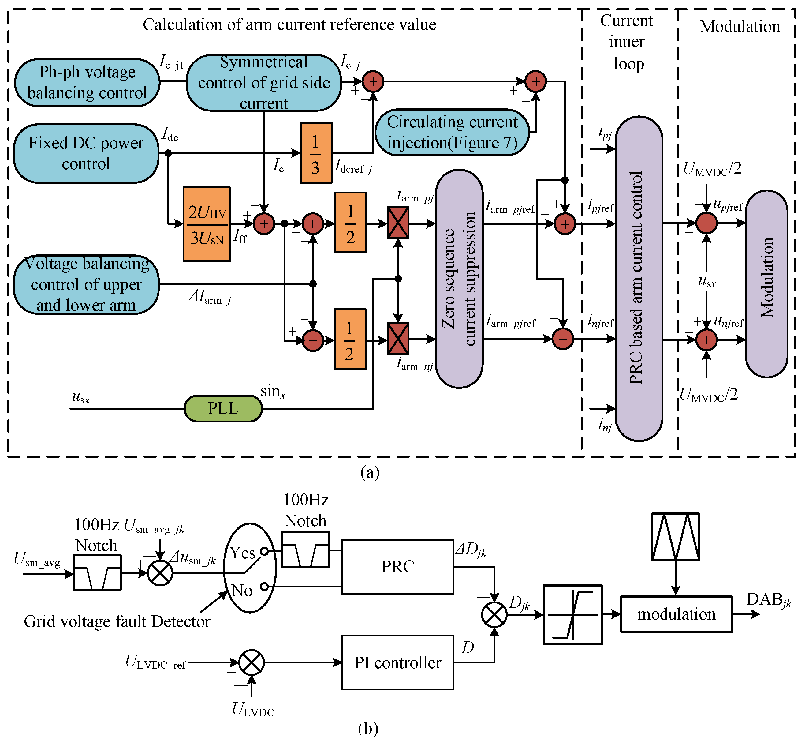
3.1. MMC-Based PRVS Strategy

(1)
Balance operation condition of the grid side voltage.
Reference [19] suggests that the ripple voltage of the submodule capacitor can be suppressed by appropriately selecting the amplitude and phase angle of the injected second harmonic circulating current. Considering phase a, after injecting the second harmonic circulating current, the current of the upper and lower arms can be expressed as follows:
i p a ( t ) = 1 3 i MVDC 1 2 I X sin ( ω t + θ ) I c cos ( 2 ω t + φ ) i n a ( t ) = 1 3 i MVDC + 1 2 I X sin ( ω t + θ ) I c cos ( 2 ω t + φ )
where I c represents the amplitude of the injected second harmonic circulating current, θ represents the power factor angle, and ϕ represents the phase angle of the injected second harmonic circulating current. According to Equation (9), the input current on the DC side of the submodule is as follows:
i SM p a ( t ) = S p a ( t ) i p a ( t ) = m I X 8 cos ( θ ) i MVDC 6 + m i MVDC 6 sin ( ω t ) I X 4 sin ( ω t + θ ) m I c 4 sin ( ω t + φ ) m I X 8 cos ( 2 ω t + θ ) I c 2 cos ( 2 ω t + φ ) + m I c 4 sin ( 3 ω t + φ )
Therefore,
I c = m I X 4 φ = θ
The second harmonic current flowing into the capacitor is zero, i.e., the second harmonic ripple voltage of the capacitor is zero. However, the injected second harmonic circulating current reference requires the amplitude and phase angle of the AC; therefore, it is based on online calculation methods, which can easily result in errors. For example, if there is a distortion in the DC or AC voltage, the circulation current obtained from the equation will also be inaccurate. To address the shortcomings of this methods, the capacitor second harmonic ripple voltage suppression method based on closed-loop control can be adopted as shown in Figure 6. First, the average voltage of 2N submodules in the same phase is monitored in real time. Then, it is subtracted from the reference value of the capacitor voltage to obtain the magnitude of the second harmonic fluctuation of the capacitor voltage. Then, the PI controller is used to obtain the circulating current reference for suppressing the second harmonic capacitor ripple voltage. In theory, the second harmonic ripple voltage cannot be fully eliminated because the PI controller cannot accurately track periodic signals.
Furthermore, to address the shortcomings of the PI controller and avoid introducing a double-frequency ripple on the MVDC side, the reference value of the circulating current output was symmetrized by the PI controller. The improved control strategy is shown in Figure 7.
(2)
Unbalanced operation condition of the grid voltage
Considering the voltage drop of phase c as an example, when the voltage asymmetry fault occurs on the grid side, the voltage amplitude of the submodule capacitor also drops proportionally under the symmetrical control of the grid side current. To maintain the symmetry of the three-phase circulating current injection, the circulating current amplitude injected by phases a and b should be consistent with that of phase c. The circulating current injection method shown in Figure 8 satisfies the requirement.

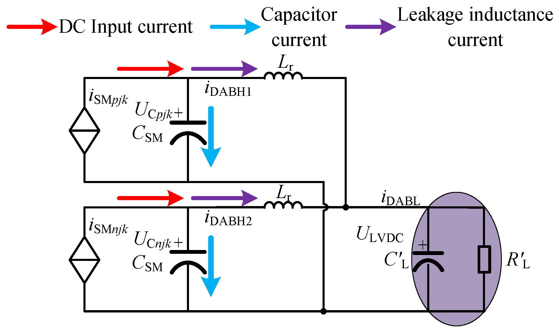
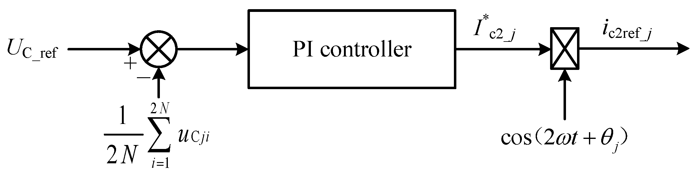
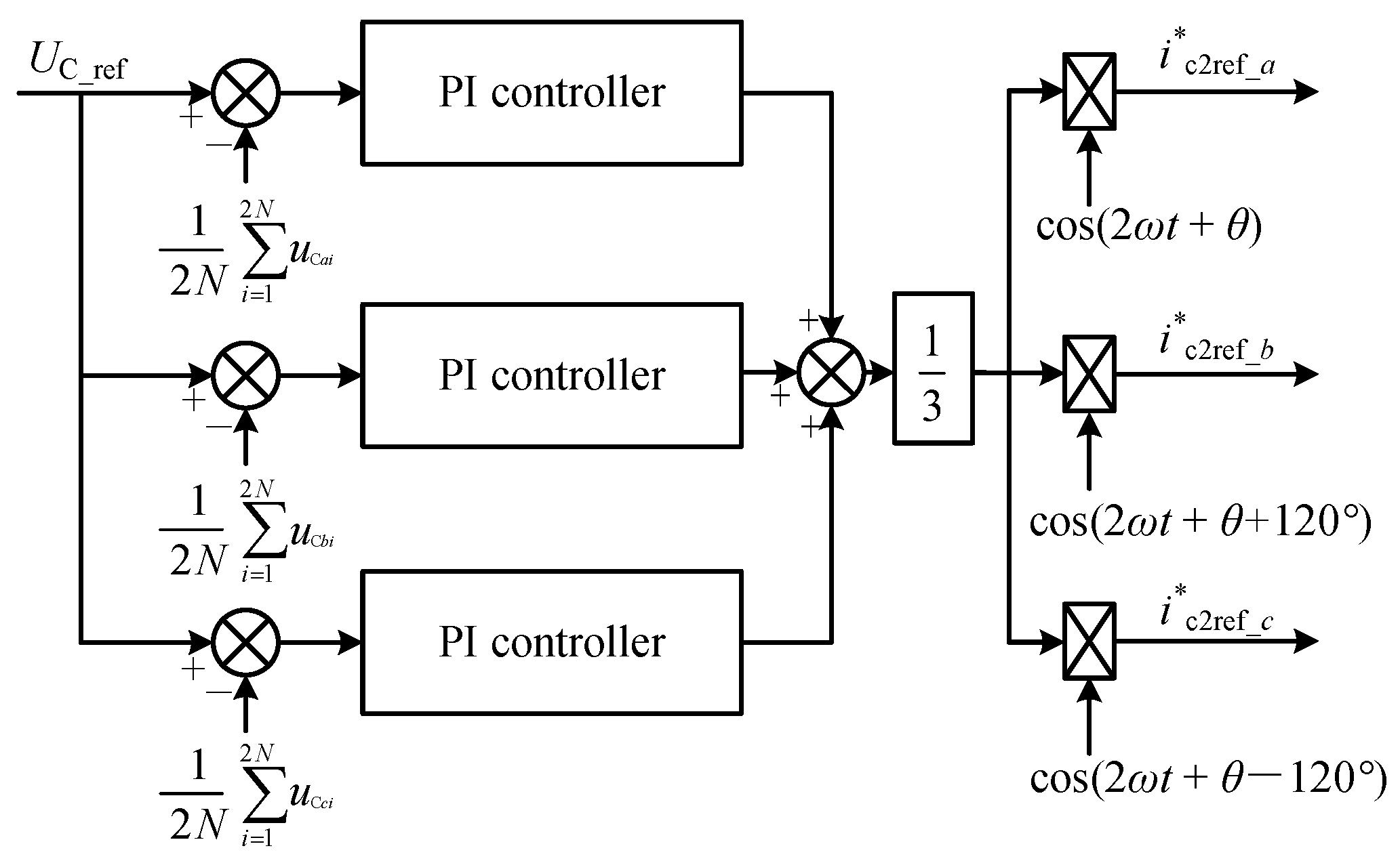
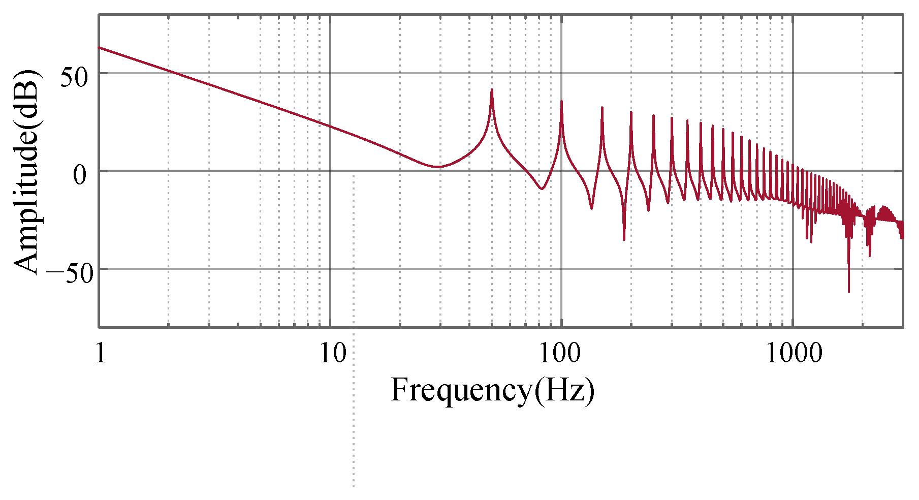
3.2. DAB-Based SRVS Strategy

Based on the above analysis, an ripple power transfer method in a balanced or unbalanced grid side voltage condition is proposed, as shown in Figure 8.
This strategy can transfer the low-frequency ripple current, which originally flows into the SM capacitor, to the LVDC load [8]. The coupling path of the capacitor ripple in the i-th submodule of each phase is upper and lower arm is shown in Figure 9. According to the symmetry of each phase is upper and lower arm, when the ripple power of the corresponding submodule of the upper and lower arm is transmitted to the coupling link, the fundamental frequency ripple component accounting for a large proportion of the DAB current will cancel out on its own. Other frequency ripples can be eliminated by merging into the LVDC bus.
We can adjust the magnitude and direction of the transfer power by changing the phase shift angle ϕ . Therefore, adopting an additional phase-shifting control strategy based on capacitor voltage closed-loop can transmit the ripple power. The repetitive controller (RC) is based on the internal model principle and has an infinite gain at periodic signals. The discrete transfer function G RC of the RC can be expressed as follows:
G RC z = K r S ( z ) z N RC + k RC 1 Q ( z ) z N RC
where K r is the gain coefficient of the RC; S ( z ) is the transfer function of the low-pass filter in the system; N RC is the number of sampling points; Q ( z ) is the transfer function of the filter used to the enhance system stability; and k RC is the number of compensations. As shown in Figure 10, PRC can suppress a multifrequency capacitor voltage ripple. Therefore, this study adopts an improved ripple suppression strategy based on PRC for MMC–PET. This method fully suppresses the capacitor ripple through the real-time feedback correction of capacitor voltage error signals at various frequencies. The PRC control parameters used are shown in Table 1.

3.3. Overall Control Strategy

The comprehensive control strategy of the MMC–PET based on arm current control is shown in Figure 11. The DC capacitor decouples MMC and DAB such that the control of both can be designed separately. For the control of MMC, this study adopts an arm current control strategy based on PRC. The strategy is simple in design and suitable for the asymmetric operation condition for the grid side voltage, including phase-locked loop, outer loop control, inner loop control, capacitor voltage balance control, and modulation. Among them, the outer loop voltage control adopts fixed power control. The inner loop control adopts arm current direct feedback control based on PRC, which can achieve zero tracking error and harmonic suppression of multifrequency arm currents (AC-side current, DC circulating current, and injected second harmonic AC circulating current). The capacitor voltage balance control adopts a hierarchical method for control. One is the phase capacitor voltage balanced control based on the DC circulating current, which can make the AC-side current symmetrical by adjusting the distribution of the DC bus power within the MMC three-phase arms when the grid voltage is asymmetric. Another approach is based on zero-sequence current suppression for arm current balance, which can eliminate the impact of inconsistent three-phase losses and zero-sequence circulating current on the MVDC side. The modulation scheme adopts phase-shifted carrier modulation with a full-bridge submodule. Specific functions of each part are discussed in reference [16].
Figure 11b shows an improved DAB phase-shifting modulation strategy. The control loop of the DAB converter includes three parts: LVDC side voltage control, ripple power control, and modulation. Voltage control based on reference voltage V LVDC_ref provides a universal phase shift angle ϕ for all DAB modules, realizing the average distribution of load power in DAB modules. PRC-based ripple power control will detect a real-time capacitor error signal and the corresponding additional phase shift angle. The modulation part adopts a triangular wave-based phase shift modulation strategy, which can obtain the square waveform for the DAB primary side through m-function programming, achieving the transmission of DC and ripple power. Because the current within the same arm remains consistent and the capacitor ripple overlaps, the additional phase shift angle used by each DAB unit within the same arm is uniform. In addition, when an asymmetric fault occurs, to maintain the stability of the LVDC side voltage during power transmission, the capacitor voltage error signal must be switched to the second harmonic notch filter position, that is a power transfer strategy conversion from the conventional ripple voltage suppression (CRVS) strategy to the SRVS strategy at this time. According to the control characteristics, the triggering signals of the DAB corresponding to different arms are different. Owing to the DAB of the upper and lower arm submodules sharing the secondary full bridge, the synthesized triggering signal should be sent to the primary side switch.
The secondary side DAB can use a unified triggering signal. The average value of all submodules U sm_avg and average value of each arm submodule U sm_avg_ jk are expressed as the following equations:
U sm _ a v g = 1 6 N sm j = a , b , c k = p , n i = 1 N sm U sm _ j k i
U sm_avg_ jk = 1 N sm j = a , b , c ; k = p , n ; i = 1 N sm U sm_ j k i

4. Simulation Verification and Analysis

4.1. Balance Operation Condition of the Grid Side Voltage

To verify the effectiveness of the coordinated suppression method for capacitor ripple voltage in the MMC–PET submodule proposed in this article, an MMC–PET topology structure based on the ISHFC of upper and lower arms shown in Figure 1 was designed on the MATLAB/Simulink simulation platform to validate this method. The high voltage AC port of the MMC–PET was connected to the MVAC distribution network. The MVDC side was replaced by a DC voltage source. A resistive load is connected to the LVDC side, and the specific simulation parameters are shown in Table 2. The simulation schematic diagram is shown in Figure 12.
The simulation timing is set as follows: when t = 0.8 s, the CRVS in [8] and proposed PRVS + SRVS strategies are added to the MMC–PET. When t = 1 s, simulation ends. The simulation results are shown in Figure 13.
Figure 13 shows that the system can operate stably before and after applying the capacitor ripple voltage suppression strategy. Picture (e1) of Figure 13A shows that the DAB-based CRVS method strategy can suppress all the submodule capacitor ripple voltage. Figure 13A(f1) shows that the current stress of the DAB secondary side switch increased from 90 A to 110 A. To solve this problem, an optimized PRVS strategy proposed in the second part is added to the simulation. Figure 13(h2) shows that the second harmonic circulating current can be correctly injected into the MMC arm current. Figure 13e,f show that the optimized suppression strategy can completely suppress the capacitor ripple voltage without significantly increasing the current stress of the ISSS switches. As shown in Figure 13B(g2), the only drawback is that the injection of circulating current leads to an increase in the arm current.

4.2. Unbalanced Condition of the Grid Side Voltage

Under the asymmetric voltage condition on the grid side, the simulation timing is as follows: when t = 0.5–0.6 s, the system operates normally, the MMC side adopts the arm current control strategy based on PRC, and the DAB adopts a single phase-shift control strategy; When t = 0.6 s, the voltage of phase c drops to 0.8 p.u.. When t = 0.9 s, the PRVS and proposed PRVS + SRVS strategies are added to the MMC–PET.
Figure 14a,b show the voltage and current waveforms on the three-phase MVAC side, respectively. Under this simulation timing, the AC-side current can achieve a stable transition under different working conditions and always maintain a symmetrical operating state, verifying the effectiveness of the AC-side symmetrical control. In Figure 14c,h, the current on the MVDC side remains relatively stable—the second harmonic ripple voltage suppression strategy based on the symmetrical circulating current injection method under symmetry or asymmetry grid side voltage conditions hardly introduces ripple currents to the MVDC side. Figure 14(d1,d2) show that the second harmonic ripple voltage on the LVDC bus decreases from ±5 V to ±1 V when the ripple suppression strategy switches to power transmission without a second harmonic ripple voltage, which verifies the effectiveness of the theoretical analysis and proposed strategy. The submodule capacitor voltage of phase a and the current stress of the ISSS switch after the application of the proposed strategy are shown in Figure 14e,f, respectively. The submodule capacitor voltage is effectively suppressed without causing an increase in the current stress of the ISSS switch regardless of whether the grid side voltage is balanced.

5. Conclusions

This study proposed an optimized method combining MMC-based PRVS with DAB-based SRVS to suppress the submodule capacitor ripple voltage in MMC-based PET systems under normal and grid fault conditions, without increasing the current stress on the ISSS switch. The following conclusions can be drawn:
  • This study proposed a modified MMC–PET topology with the ISHFC of upper and lower arms, which reduced the number of full-bridge modules and made the structure more compact.
  • The MMC-based PRVS method coordinated with the DAB-based SRVS strategy based on PRC can provide real-time feedback correction for multiple frequency capacitor ripple voltages, and then the ripple power is transmitted to the LVDC bus by the DAB, significantly improving the suppression effect of voltage ripple in the submodule capacitor and second-order voltage ripple in the LVDC bus under normal and grid fault conditions. The second harmonic ripple voltage on the LVDC bus can be decreased from ±5 V to ±1 V with the proposed SRVS method under the asymmetric grid voltage condition.
  • The proposed method can effectively eliminate the fundamental and second harmonic components of the submodule capacitor ripple voltage without increasing the current stress of the ISSS switch, thereby reducing the volume and cost of the device; simulation results showed that the peak-to-peak submodule capacitor ripple voltage was reduced from 232 V to 10 V, while the peak current of the isolation-stage secondary side (ISSS) switch was limited to 90 A.

Author Contributions

Conceptualization, J.L. and Y.W.; methodology, J.L.; software, X.J.; validation, X.J. and Z.W.; formal analysis, X.J. and Z.W.; investigation, X.J., Y.L. and X.Z.; writing—original draft preparation, X.J.; writing—review and editing, Z.W., Y.L. and X.Z.; supervision, J.L. All authors have read and agreed to the published version of the manuscript.

Funding

This research was funded by the National Natural Science Foundation of China under Grant No. 52307148.

Data Availability Statement

The original contributions presented in this study are included in the article. Further inquiries can be directed to the corresponding author.

Conflicts of Interest

Authors Yongxiang Liu and Xinbing Zhu were employed by the company Xuchang Intelligent Building, Xuchang Intelligent Relay Co., Ltd. The remaining authors declare that the research was conducted in the absence of any commercial or financial relationships that could be construed as a potential conflict of interest.

References

  1. Núñez, R.A.; Posada, J.; Unsihuay-Vila, C.; Pinzón-Ardila, O. Review of Smart Transformer-Based Meshed Hybrid Microgrids: Shaping, Topology and Energy Management Systems. IEEE Access 2023, 11, 130165–130185. [Google Scholar]
  2. Deng, J.; Wang, X.; Tao, C.; Meng, F. An Energy Router Based on Multi-Hybrid Energy Storage System with Energy Coordinated Management Strategy in Island Operation Mode. Renew. Energy 2023, 212, 274–284. [Google Scholar] [CrossRef]
  3. Ma, D.; Chen, W.; Shu, L.; Qu, X.; Hou, K. A MMC-Based Multiport Power Electronic Transformer With Shared Medium-Frequency Transformer. IEEE Trans. Circuits Syst. II 2021, 68, 727–731. [Google Scholar] [CrossRef]
  4. Lu, S.; Deng, J.; Li, S.; Shao, Y.; Li, K. A Multiport Power Electronic Transformer Based on Three-Phase Four-Arm Full-Bridge Modular Multilevel Converter. IEEE Trans. Power Electron. 2024, 39, 16174–16186. [Google Scholar] [CrossRef]
  5. Li, Z.; Pei, Y.; Lu, C.; Wang, L.; Cao, W.; Leng, Z. An Analytical Closed-Loop Steady-State Model for Modular Multilevel Converters. IEEE Trans. Ind. Electron. 2025, 1–11. [Google Scholar] [CrossRef]
  6. Fawzi, M.; Abdelsalam, I.; Ahmed, A.A.; Maksoud, S.A.A. A Modified Phase Shift Control of the Dual Active Bridge-Based Modular Power Electronic Transformer to Minimize the LVdc Side Voltage Ripples Under Unbalanced Load Conditions. IEEE Access 2022, 10, 81309–81322. [Google Scholar] [CrossRef]
  7. Zhu, X.; Hou, J.; Zhang, B. A Multiport Power Electronic Transformer With MVDC Integration Interface for Multiple DC Units. IEEE Trans. Ind. Electron. 2024, 71, 10704–10715. [Google Scholar] [CrossRef]
  8. Zhou, J.; Zhang, J.; Wang, J.; Zang, J.; Shi, G.; Feng, X. Design and Control of Power Fluctuation Delivery for Cell Capacitance Optimization in Multiport Modular Solid-State Transformers. IEEE Trans. Power Electron. 2021, 36, 1412–1427. [Google Scholar] [CrossRef]
  9. Li, Z.; Pei, Y.; Wang, L.; Zhao, L.; Pei, L.; Cao, W. A Comprehensive Closed-Loop Voltage Ripple Control Scheme for Modular Multilevel Converter-Based Power Electronic Transformers. IEEE Trans. Power Electron. 2023, 38, 15225–15241. [Google Scholar] [CrossRef]
  10. Goudarzitaemeh, S.; Pahlevani, M. Extended Phase Shift Control of a Novel Bidirectional DC–DC Converter With Direct Power Transfer. IEEE J. Emerg. Sel. Top. Power Electron. 2024, 12, 4521–4537. [Google Scholar] [CrossRef]
  11. Liu, B.; Yu, T.; Ge, L.; Niu, J. Feedforward Compensation for Phase-Shifted Full-Bridge DC–DC Converter Under Peak Current Mode Control. IEEE Trans. Power Electron. 2024, 39, 6840–6851. [Google Scholar] [CrossRef]
  12. Akbar, S.M.; Hasan, A.; Watson, A.J.; Wheeler, P. Based Transformer Loss Analysis for Dual Active Bridge DC–DC Converter Using Triple Phase Shift Modulation. IEEE J. Emerg. Sel. Top. Power Electron. 2022, 10, 4347–4360. [Google Scholar] [CrossRef]
  13. Hu, Y.; Li, Z.; Zhang, H.; Zhao, C.; Gao, F.; Luo, L. High-Frequency-Link Current Stress Optimization of Cascaded H-Bridge-Based Solid-State Transformer With Third-Order Harmonic Voltage Injection. IEEE J. Emerg. Sel. Top. Power Electron. 2021, 9, 1027–1038. [Google Scholar] [CrossRef]
  14. Bandaru, T.; Samajdar, D.; Varma, P.B.S.; Bhattacharya, T.; Chatterjee, D. Optimum Injection of Second Harmonic Circulating Currents for Balancing Capacitor Voltages in Hybrid MMC during Reduced DC Voltage Conditions. IEEE Trans. Ind. Appl. 2020, 56, 1649–1660. [Google Scholar] [CrossRef]
  15. Xu, J.; Deng, W.; Gao, C.; Lu, F.; Liang, J.; Zhao, C. Dual Harmonic Injection for Reducing the Submodule Capacitor Voltage Ripples of Hybrid MMC. IEEE J. Emerg. Sel. Top. Power Electron. 2021, 9, 3622–3633. [Google Scholar] [CrossRef]
  16. Ou, Z.; Wang, G.; Zhang, L. Modular Multilevel Converter Control Strategy Based on Arm Current Control Under Unbalanced Grid Condition. IEEE Trans. Power Electron. 2018, 33, 3826–3836. [Google Scholar] [CrossRef]
  17. Liu, D.; Wang, G.; Ou, Z.; Liu, J. A Control Strategy of MMC Battery Energy Storage System Based on Arm Current Control. In Proceedings of the 2018 International Power Electronics Conference (IPEC-Niigata 2018 -ECCE Asia), Niigata, Japan, 20–24 May 2018; pp. 1376–1380. [Google Scholar]
  18. Song, Q.; Liu, W.; Li, X.; Rao, H.; Xu, S.; Li, L. A Steady-State Analysis Method for a Modular Multilevel Converter. IEEE Trans. Power Electron. 2013, 28, 3702–3713. [Google Scholar] [CrossRef]
  19. Vasiladiotis, M.; Cherix, N.; Rufer, A. Accurate Capacitor Voltage Ripple Estimation and Current Control Considerations for Grid-Connected Modular Multilevel Converters. IEEE Trans. Power Electron. 2014, 29, 4568–4579. [Google Scholar] [CrossRef]
Figure 1. Distribution grid based on a PETs.
Electronics 14 02385 g001
Figure 2. Typical topology of the MMC-PET.
Electronics 14 02385 g002
Figure 3. Schematic diagram of the MMC–PET topology with upper and lower arm coupling.
Electronics 14 02385 g003
Figure 4. Schematic diagram of the k-th multiport DC–DC structure.
Electronics 14 02385 g004
Figure 5. Equivalent model of a multiport DC–DC converter.
Electronics 14 02385 g005
Figure 6. Circulating current injection method based on capacitor voltage closed-loop.
Electronics 14 02385 g006
Figure 7. Symmetric circulating current injection method based on capacitor voltage closed-loop control.
Electronics 14 02385 g007
Figure 8. Ripple power transfer method in a balanced or unbalanced grid side voltage condition. (a) Balanced operating condition (b) Unbalanced operating condition.
Electronics 14 02385 g008
Figure 9. Coupling path of a capacitor ripple in the i-th submodule of each phase’s upper and lower arm.
Electronics 14 02385 g009
Figure 10. Bode diagram of the transfer function for proportional repetitive control.
Electronics 14 02385 g010
Figure 11. Upper and lower arm coupling-based MMC–PET comprehensive control strategy. (a) Arm current control strategy for MMC (b) Improved DAB phase shift modulation strategy with SRVS.
Electronics 14 02385 g011
Figure 12. Diagram of the simulation model.
Electronics 14 02385 g012
Figure 13. Simulation waveforms based on the MMC–PET topology shown in Figure 1 with (A) CRVS strategy; (B) proposed PRVS strategy; (a1,a2) voltage on the three-phase MVAC side; (b1,b2) current on the three-phase MVAC side; (c1,c2) current on the MVDC side; (d1,d2) voltage on the LVDC side; (e1,e2) submodule capacitor voltage of phase a; (f1,f2) the current stress of the DAB secondary side switch; (g1,g2) upper arm current stress of phase a in the MMC; (h1,h2) circulating currents of phases (a1,a2c1,c2).
Electronics 14 02385 g013
Figure 14. Simulation waveforms based on the MMC–PET topology structure shown in Figure 1 under the asymmetric grid voltage condition with (A) proposed PRVS strategy; (B) proposed PRVS + SRVS strategy; (a1,a2) voltage on the three-phase MVAC side; (b1,b2) current on the three-phase MVAC side; (c1,c2) current on the MVDC side; (d1,d2) voltage on the LVDC side; (e1,e2) submodule capacitor voltage of phase a; (f1,f2) the current stress of the DAB secondary side switch; (g1,g2) upper arm current stress of phase a in MMC; (h1,h2) circulating currents of phases (a1,a2c1,c2).
Electronics 14 02385 g014
Table 1. Parameters of the PRC.
ParametersValue in Improved DAB Phase Shift Modulation StrategyValue in Arm Current Control
N rc 200200
K r 0.970.97
k RC 113
S ( z ) 0.02088 z 2 + 0.04176 z + 0.02088 z 2 1.651 z + 0.7342 0.287 z + 0.1435 z 2 + 0.3213 z 0.891
K p 0.11.5
Table 2. MMC–PET model simulation and control parameters.
ParametersValue
Rated power S N /MW1.5
Medium voltage AC line voltage/kV10
Medium voltage DC voltage/kV20
Number of arm submodules10
Submodule DC voltage/V2000
Submodule capacitance/μF600
Arm inductance/mH10
Grid side inductance/mH10
Grid side resistance/ Ω 0.001
Arm inductance/mH40
Arm resistance/ Ω 0.05
MMC submodule switching frequency/kHz1
MMC modulation methodSPWM
Transformer isolation stage parameters
Low voltage DC voltage/V750
DAB switching frequency/kHz5
DAB leakage inductance/mH0.5
HFT conversion ratio2.67:1
Low voltage DC-side capacitance/mF30
Load resistance/ Ω 1.8
Control parameters
PI of Ph-ph voltage balancing control1, 40
PI of Circulating current injection1.33, 41.6
PI of Fixed DC power control0.003, 1000
PI of voltage balancing control of upper and lower arm1.33, 41.6
PI of LVDC voltage control0.03, 10
Disclaimer/Publisher’s Note: The statements, opinions and data contained in all publications are solely those of the individual author(s) and contributor(s) and not of MDPI and/or the editor(s). MDPI and/or the editor(s) disclaim responsibility for any injury to people or property resulting from any ideas, methods, instructions or products referred to in the content.

