Next Article in Journal
One Possible Path Towards a More Robust Task of Traffic Sign Classification in Autonomous Vehicles Using Autoencoders
Previous Article in Journal
Safety Management Technologies for Wireless Electric Vehicle Charging Systems: A Review
Previous Article in Special Issue
Insight into Optimally Noise- and Signal-Matched Three-Stage LNAs and Effect of Inter-Stage Mismatch
 
 
Due to scheduled maintenance work on our database systems, there may be short service disruptions on this website between 10:00 and 11:00 CEST on June 14th.
Article

A Low-Power Differential Temperature Sensor with Chopped Cascode Transistors and Switched-Capacitor Integration

by
Junyi Yang
1,
Thomas Gourousis
1,
Mengting Yan
2,
Ruyi Ding
1,
Ankit Mittal
1,
Milin Zhang
1,
Francesco Restuccia
1,
Aatmesh Shrivastava
1,
Yunsi Fei
1 and
Marvin Onabajo
1,*
1
Department of Electrical and Computer Engineering, Northeastern University, Boston, MA 02115, USA
2
Analog Devices Inc., Chandler, AZ 85225, USA
*
Author to whom correspondence should be addressed.
Electronics 2025, 14(12), 2381; https://doi.org/10.3390/electronics14122381
Submission received: 21 March 2025 / Revised: 5 June 2025 / Accepted: 6 June 2025 / Published: 11 June 2025
(This article belongs to the Special Issue Advances in RF, Analog, and Mixed Signal Circuits)

Abstract

:
Embedded differential temperature sensors can be utilized to monitor the power consumption of circuits, taking advantage of the inherent on-chip electrothermal coupling. Potential applications range from hardware security to linearity, gain/bandwidth calibration, defect-oriented testing, and compensation for circuit aging effects. This paper introduces the use of on-chip differential temperature sensors as part of a wireless Internet of Things system. A new low-power differential temperature sensor circuit with chopped cascode transistors and switched-capacitor integration is described. This design approach leverages chopper stabilization in combination with a switched-capacitor integrator that acts as a low-pass filter such that the circuit provides offset and low-frequency noise mitigation. Simulation results of the proposed differential temperature sensor in a 65 nm complementary metal-oxide-semiconductor (CMOS) process show a sensitivity of 33.18 V / ° C within a linear range of ± 36.5 m ° C and an integrated output noise of 0.862 mV rms (from 1 to 441.7 Hz) with an overall power consumption of 0.187 mW . Considering a figure of merit that involves sensitivity, linear range, noise, and power, the new temperature sensor topology demonstrates a significant improvement compared to state-of-the-art differential temperature sensors for on-chip monitoring of power dissipation.

1. Introduction

Electrothermal coupling is a natural phenomenon that occurs due to the power dissipation of circuits on a die surface. It occurs when there is a transfer of heat between the circuit and the semiconductor substrate due to the circuit’s power consumption ( Power = Voltage × Current ) and the Joule effect [1,2]. This physical phenomenon generates a temperature change relative to the ambient chip temperature in the vicinity of the circuit. As part of the electrothermal coupling, there is a multiplication of voltages and currents within on-chip devices, which in turn creates power/temperature components at DC and various other frequencies. As experimentally validated in [3], thermal coupling has low-pass filtering characteristics, and measurements are usually performed up to 10 kHz. Furthermore, various approaches have been proposed to model and simulate electrothermal coupling effects using standard circuit simulators, such as in [1,4,5]. In these approaches, the silicon substrate is typically modeled with a thermal resistor–capacitor (RC) network for joint electrothermal coupling simulations with the electrical circuits under evaluation. As a result, the thermal profile of a fabricated integrated circuit (IC) can be a valuable source of information in monitoring the operation states and the performance of on-chip devices [1,2]. To monitor the slowly varying temperature gradients, on-chip differential temperature sensors can be employed, which are often found in applications such as tracking and compensating for the aging effects of power amplifiers [6], defect-oriented circuit testing [7], measuring the center frequency and 3 dB bandwidth of amplifiers [8,9], monitoring radio frequency (RF) circuit power and linearity [10], and on-chip hardware Trojan detection [11,12,13]. In the above-mentioned applications, the differential temperature sensors utilize bipolar junction transistors (BJTs) in order to sense the temperature gradients on-chip. Nevertheless, metal-oxide-semiconductor field-effect transistor (MOSFETs) also naturally have temperature-dependent parameters [14], such as their threshold voltage ( V TH ) and electron mobility ( μ ), and they can be utilized as the sensing elements for differential temperature sensors [15,16,17]. Compared with conventional thermal/power profile extraction approaches that require the use of either infrared imaging of the exposed die surface [18] or active power-path current measurements [19], on-chip differential temperature sensors provide a non-invasive monitoring solution that does not require any electrical connections to the circuit under test (CUT), thereby avoiding the connection of any devices or switches along the signal path [12]. Furthermore, there is no need for any additional off-chip connections, which eases integration into SoCs. Since the information of interest is located at low frequencies, flicker noise and DC offsets are the key sources of errors, which require additional design considerations. One more important aspect to note is that in differential temperature sensors, the temperature difference is amplified with a high gain due to the differential operation, whereas the ambient chip temperature is suppressed because it appears as a common-mode signal [1].
The proposed two-stage fully differential temperature sensor is shown in Figure 1. The power dissipated from the CUT activities leads to a temperature change ( T s ), relative to the ambient chip temperature, within its adjacent area, which modulates the base-emitter ( V BE ) voltage of the sensing bipolar junction transistor (BJT) [1,10] labeled as Q 1 in Figure 1. In the first stage, a differential current ( I in = i IN + i IN ) is generated due to the temperature imbalance of Q 1 and Q 2 ( Q 1 and Q 2 are at different locations on the die), which is further amplified by the cascode differential amplifier with chopper stabilization (i.e., stage 1). In contrast to previous designs [10,11,12,13], the proposed circuit generates an output voltage by means of a cascode amplifier structure instead of using feedback resistors, which avoids the noise generated by the feedback resistors while achieving high sensitivity with low power and noise. Furthermore, in this design, the flicker noise of the cascode load is reduced significantly with the help of chopper stabilization. The second stage consists of a switched-capacitor integrator that suppresses the up-converted low-frequency noise.
This paper is organized as follows: In Section 2, a target application for the proposed differential temperature sensor is described as an example of the emerging opportunities for non-invasive power-based monitoring. In Section 3, the proposed differential temperature sensor is analyzed, and a discussion of key insights and design considerations is provided. To validate the circuit’s performance, simulation results are presented in Section 4. Section 5 provides the concluding remarks.

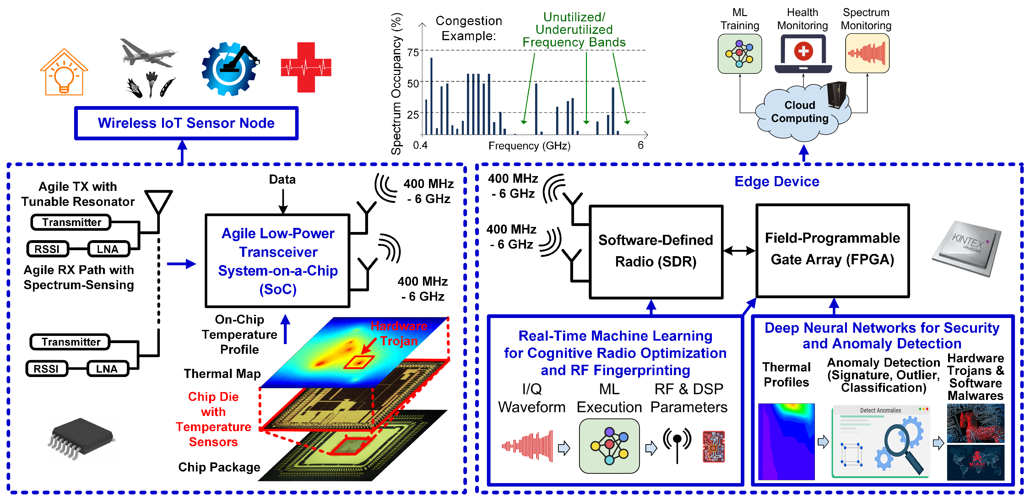
2. Target Application

Figure 2 depicts a potential application for the aforementioned differential temperature sensing approach, which is a system under development. This envisioned system incorporates a resilient, spectrum-agile low-power Internet of Things (IoT) System-on-Chip (SoC) with RF spectrum sensing at the sensor node, together with coordinated optimization and enhanced security at the edge device. On the wireless IoT sensor node side, the temperature change of the CUT is monitored for potential anomalous behavior with the help of multiple sensing BJT devices that are placed across the die and multiplexed to a single sensor circuit core as in [13]. In this approach, only one sensing BJT is selected at a time using analog multiplexers and decoders as in [12,13], which implies that the sensing BJTs are time-sharing one sensor core. The measured temperature gradients are wirelessly transmitted to the edge device where a machine learning (ML) algorithm, running on a Field-Programmable Gate Array (FPGA), processes the data to identify potential undesirable behaviors. More specifically, it was established in prior work [20] that an Autoencoder-based ML algorithm can identify the presence and potential location of HTs with 90% accuracy when the Trojan power consumption is as low as 2.5% of the CUT. In addition, besides its possible utilization for hardware Trojan detection in the discussed SoC, the differential temperature sensing approach can also be used as part of a broader anomaly detection system to monitor different RF circuit performance metrics such as the aging effects of power amplifiers [6], potential defects in low-noise amplifiers (LNAs) [7], the linearity of amplifiers [10], and the center frequency and 3 dB bandwidth of power amplifiers [8,9]. In such applications and in the envisioned SoC, the on-chip temperature sensors allow the detection of local differential temperature variations through electrothermal coupling due to the power dissipation in nearby devices, thereby serving as power detectors.
With regard to the capabilities of spectrum sensing in the envisioned system, it was demonstrated in [21] that by leveraging an on-chip analog spectrum sensor and a deep learning (DL) algorithm, empty spectrum can be identified in less than 1 μ s to opportunistically initiate communication in available frequency bands. Additionally, fine-grained signal detection among channels in the 0.4 6 GHz range can be achieved for a number of different modulation signals. In IoT applications, a variety of different transceiver architectures have been reported with a wide range of power consumption (e.g., from 80 μ W to 7 mW in [22,23,24,25]). It is envisioned that the measurements with the sensors will be performed periodically instead of continuously in many applications in order to save power.
The block diagram of the anticipated sensor signal processing path for the agile low-power SoC is displayed in Figure 3. It includes the proposed differential temperature sensor (i.e., stage 1 and stage 2 in Figure 1), an analog-to-digital converter (ADC), and a radio frequency transmitter (RF-TX). The differential signal generated in stage 1 by the BJT-based differential amplifier with cascode gain stage is further amplified by the integrator gain in stage 2. Implementing stage 2 of the differential temperature sensor with a switched-capacitor integrator enables the ability to reuse the clock signal of the ADC by deriving the switching and reset frequencies with on-chip digital dividers. In practice, an RF-TX can be employed to transmit the sensed data to the edge device in Figure 2 for the detection of hardware Trojans and, potentially, other anomalies.

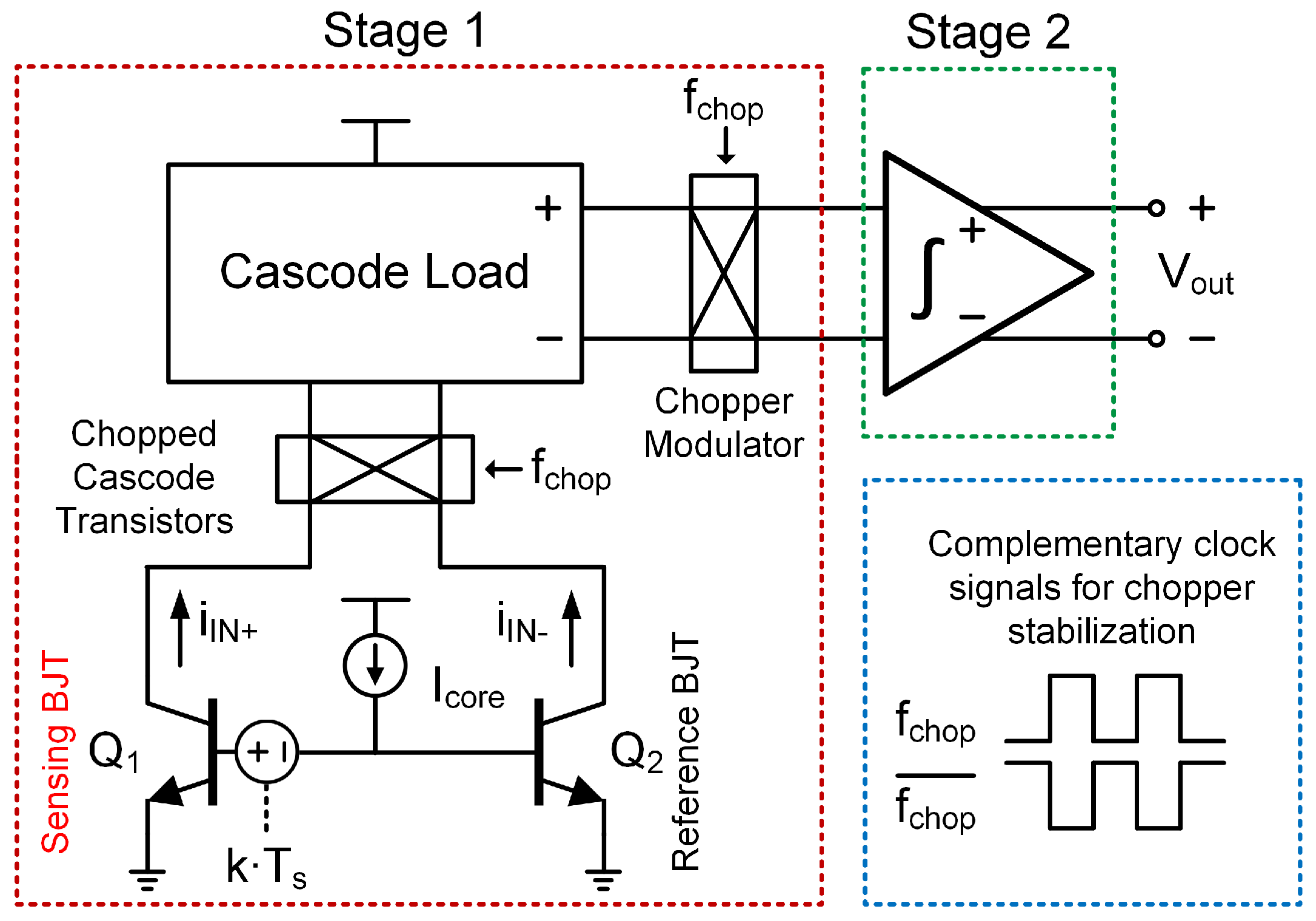
3. Differential Temperature Sensor Design

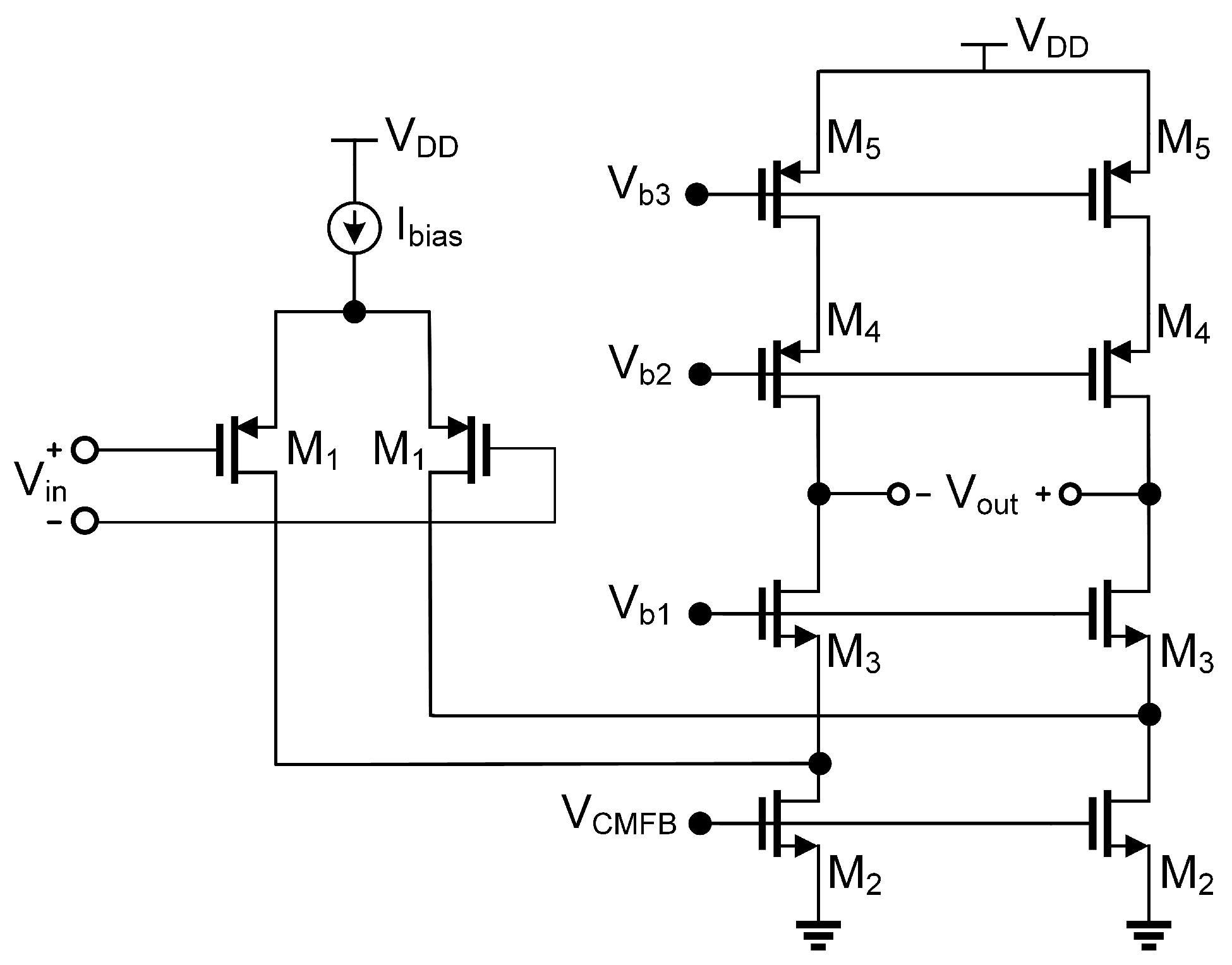
3.1. BJT-Based Cascode Differential Amplifier

Figure 4a depicts the schematic of the proposed BJT-based cascode differential amplifier, consisting of M 1 , M 2 , M 3 , and two vertical N+ diffusion/Pwell/deep-Nwell (NPN) BJTs that are available in standard 65 nm CMOS processes. In addition, there are two calibration current sources: I CAL + and I CAL . Sensing device Q 1 is located close to the CUT, while Q 2 , which is identical to Q 1 , is placed at a reference location with a steady ambient chip temperature. More specifically, as with other differential temperature sensors [1,10,13], Q 2 should be placed at least 150   μ m away from digital circuits with high switching activity and from analog circuits with high dynamic power levels. Thermal coupling effects from the CUT lead to a temperature change ( T s ) at the sensor location in the adjacent area of the CUT. To mimic such temperature change using a standard electrical simulator [26], an ideal voltage-controlled voltage source with a gain of k = 1.4 mV / K is employed to model the temperature-dependent base-emitter voltage ( V BE ) of the BJTs [1].
The sensing and reference BJTs form a differential pair in the first amplification stage, where the temperature difference is the effective input signal as it leads to changes of the base-emitter voltages that ultimately change the differential collector currents. The collector currents flow through the high output impedance ( R out ) of the amplifier that is approximated by Equation (1), thus generating a differential output voltage. The temperature-to-voltage gain ( A v 1 ) of this structure is given by Equation (2), where g m 1 , g m 2 , g m 3 , g mQ , r ds 1 , r ds 2 , r ds 3 , and r ce are the transconductances and output resistances (drain-to-source or collector-to-emitter) of MOSFETs and BJTs, respectively.
R o u t ( g m 2 r d s 2 r d s 1 / / g m 3 r d s 3 r c e )
A v 1 V o u t T s k · g m Q · R o u t
A common-mode feedback (CMFB) circuit similar to [10] was designed to regulate the output common-mode voltage of the sensor by controlling the gate voltages of the transistors labeled M 1 . Various approaches have been reported for robust process–voltage–temperature (PVT)-insensitive generation of a stable power supply ( V DD ), bias voltages, and bias currents over wide temperature ranges [27,28,29,30,31,32]. These voltage/current references cover a temperature range from 20   ° C all the way to 100   ° C with a temperature coefficient of less than 100 ppm / ° C , both with and without trimming. For this reason, the bias currents and voltages in this design are assumed constant during the temperature measurement. Furthermore, as can be observed from the simulation results in Section 4, any differential DC offsets from bias variations are suppressed by the calibration prior to the measurement.

3.2. Noise Analysis of the BJT-Based Cascode Differential Amplifier

The drain-to-source current-referred thermal and flicker noise contributions of M 1 ( i n , M 1 2 ¯ = 4 k B T γ g m 1 + K p g m 1 2 W 1 L 1 C ox f ), when referred to the output of the BJT-based cascode differential amplifier, can be expressed by Equations (3) and (4), where k B is the Boltzmann’s constant, T is the absolute temperature in Kelvin, γ is the noise coefficient of M 1 , W 1 and L 1 are the width and length of M 1 , K p is a manufacturing process-dependent constant, C ox is the gate oxide capacitance per unit area, and f stands for frequency. The noise contributions of M 2 and M 3 can be ignored because they are cascode transistors with high drain-to-source resistance and as such have negligible impact on the overall output noise [33]. The noise contributions of the calibrations currents can be modeled as i n , CAL 2 ¯ , which when referred to the output of stage 1, can be described by Equation (5).
The collector-referred noise current density of Q 1 , 2 ( i n , Q 1 , 2 2 ¯ ) can be expressed by Equation (6) based on [34]. I B and I C are the base and collector currents, respectively. K is a manufacturing process-dependent constant, and β is the common-emitter current gain. In this design, I B = I core / 2 = 10 μ A and β = 6.2. The BJT noise current flows into the output impedance of the proposed amplifier to generate the output-referred noise contribution of Q 1 , 2 that is estimated using Equation (7).
V M 1 , t h e r m a l 2 ¯ 8 k B T γ g m 1 · ( g m 2 r d s 2 r d s 1 / / g m 3 r d s 3 r c e ) 2
V M 1 , f l i c k e r 2 ¯ 2 K p g m 1 2 W 1 L 1 C o x f · ( g m 2 r d s 2 r d s 1 / / g m 3 r d s 3 r c e ) 2
V n , C A L 2 ¯ i n , C A L 2 ¯ · ( g m 2 r d s 2 r d s 1 / / g m 3 r d s 3 r c e ) 2
I n , Q 1 , 2 2 ¯ 2 q I B β 2 + K I B f β 2 + 2 q I C
V n , Q 1 , 2 2 ¯ I n , Q 1 , 2 2 ¯ · ( g m 2 r d s 2 r d s 1 / / g m 3 r d s 3 r c e ) 2
Based on simulations, the flicker noise (i.e., Equation (4)) from M 1 is the dominant noise source of the BJT-based cascode differential amplifier. To reduce the noise generated by M 1 , a chopper stabilization technique is applied [35]. In Figure 4, M 3 A and M 3 B are identical to M 3 , and they replace M 3 in the first amplifier stage. These cascode transistors ( M 3 A and M 3 B ) are activated in an alternating fashion with a chopping frequency of f chop and thus form the chopped cascode transistors. Therefore, the chopped cascode transistors act as a modulator that up-converts the signal generated by Q 1 and Q 2 and the calibration currents ( I CAL + , I CAL ) to the frequency band around f chop . The gate voltages of M 3 A and M 3 B are alternately biased between V b 2 (900 mV ) and 0 V, driven by the non-overlapping clock signals, f chop and f chop ¯ . More specifically, as can be seen in Figure 4b, V G A = 0 V and V G B = 900 mV , which implies that M 3 B transistors are activated while M 3 A transistors are disabled. In Figure 4c, V G A = 900 mV and V G B = 0 V such that M 3 A transistors are activated while M 3 B transistors are disabled. Note that when the cascode transistors are activated, they have the same operating point (biased in the saturation region) as regular cascode transistors instead of operating in the triode region as would be the case with standard switches used for chopping. On the other hand, the control switches, S 1 and S 2 , alternate between cutoff and triode regions of operation. Switches labeled S 1 are implemented with PMOS transistors, and switches labeled S 2 are realized with NMOS transistors. Conventionally, the up-converting chopper modulator would be located in series with the cascode transistors ( M 3 ) [36,37,38]. However, typical switching transistors tend to be large in size to achieve acceptable series resistance. For example, in this design, transistors in a conventional up-converting chopper modulator would require a 20 times larger W / L ratio than the cascode transistors ( M 3 ) to maintain a voltage drop of less than 10 mV across the chopper modulator. In contrast, reusing M 3 A and M 3 B as chopped cascode transistors to form the up-converting chopper modulator excludes the resistance of the conventional chopper modulator from the signal path to save area and voltage headroom. The output chopper modulator is placed at the drain of the M 2 transistors in Figure 4 in order to down-convert the temperature information. Since the flicker noise in Equation (4) of M 1 is only modulated by the down-converting chopper modulator, its equivalent output-referred noise is converted to odd harmonics of f chop and hence can be filtered out by the switched capacitor integrator in stage 2. According to [39], the output noise of stage 1 can be estimated as
V n , o u t , s t 1 2 ¯ 8 π 2 ( V M 1 , f l i c k e r 2 ¯ + V M 1 , t h e r m a l 2 ¯ ) · ( 1 + f c f c h o p ) + V Q 1 , 2 , B J T 2 ¯ + V n , C A L 2 ¯
where f c is the corner frequency of the flicker noise of M 1 , and f c h o p = 10 kHz in this design.

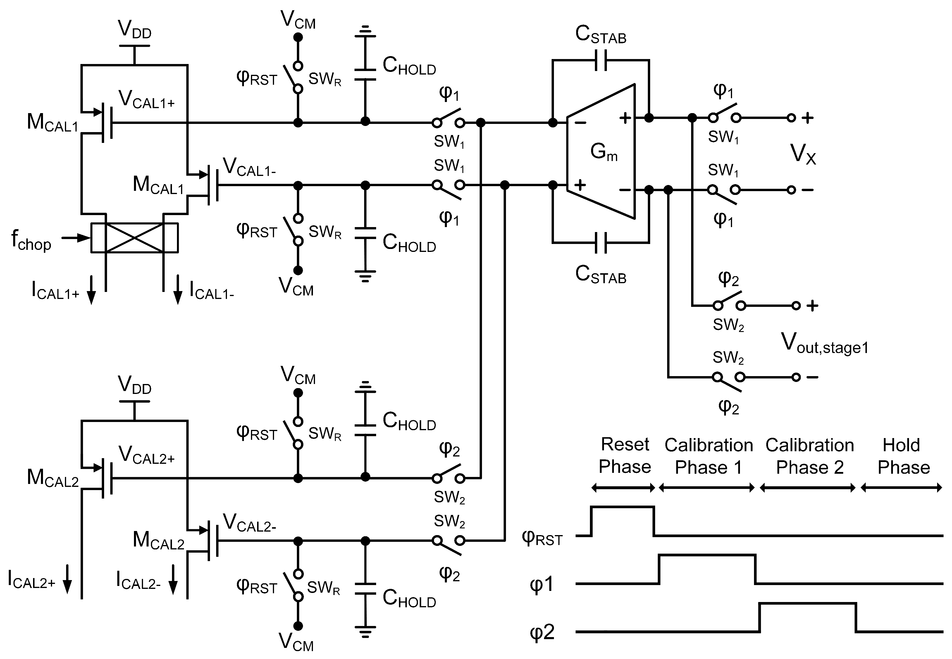
3.3. On-Chip Calibration Circuit

Mismatch due to process variation and on-chip thermal gradient can generate signal offsets, which in turn can saturate the high gain differential temperature sensor. Thus, prior to each temperature measurement, an on-chip calibration circuit is utilized to compensate for stage 1 mismatch.
The calibration circuit with its control signals is depicted in Figure 5. The calibration circuit consists of the following three components: three sets of switches labeled SW 1 , SW 2 and SW 3 to activate and deactivate the calibration circuits; two pairs of transistors ( M CAL 1 and M CAL 2 ) that inject calibration currents (in Figure 4: I CAL + = I CAL 1 + + I CAL 2 + , and I CAL = I CAL 1 + I CAL 2 ) into the BJT-based cascode differential amplifier; and a two-stage calibration amplifier that senses the differential signal from the first stage and generates two pairs of differential gate control voltages ( V CAL 1 and V CAL 2 ) for M CAL 1 and M CAL 2 in Figure 5, along with a pair of holding capacitors ( C HOLD ) to maintain V CAL during regular operation of the differential temperature sensor.
As shown in Figure 5, three main control signals define the four phases of the calibration. In the reset phase, I CAL 1 and I CAL 2 are reset to 0 A. During this phase, ϕ R S T is high, while ϕ 1 and ϕ 2 are low, which closes SW R and opens SW 1 and SW 2 . In this phase, C HOLD is connected to V CM . Next, in calibration phase 1, the offset contributions of the chopped PMOS cascode load devices are suppressed. During this phase, ϕ 1 is high, while ϕ R S T and ϕ 2 are low, which closes SW 1 and opens SW R and SW 2 . The calibration amplifier is connected to V X = V X + V X in Figure 4. The amplifier generates a calibration voltage V CAL 1 ; hence, M CAL 1 inject a calibration current I CAL 1 into stage 1. A down-converting chopper modulator is placed in series with M CAL 1 transistors in order to modulate I CAL 1 with the same chopping frequency f chop as in the main amplifier. In calibration phase 2, the electrical offset contributions of the BJT devices and any sensed on-chip thermal gradients are reduced through the calibration without chopping. During this phase, ϕ 2 is high, while ϕ R S T and ϕ 1 are low, which closes SW 2 and opens SW R and SW 1 . The calibration amplifier is connected to the output of stage 1, sensing the down-converted signal after the modulator. The amplifier generates a calibration voltage V CAL 2 . Consequently, I Cal 2 is produced by M CAL 2 and injected into stage 1. In the hold phase, ϕ R S T , ϕ 1 , and ϕ 2 are low, which opens SW R , SW 1 , and SW 2 . The calibration amplifier is disconnected as well, and the holding capacitors ( C HOLD ) retain the gate control voltages ( V CAL 1 and V CAL 2 ). In this phase, the differential temperature sensor is activated for temperature-sensing measurements.
This calibration loop is similar to the one of the prototype chips measured in [13] but is designed specifically for this new sensor circuit. The calibration amplifier is a two-stage amplifier (Figure 6) similar to [13], with a common-mode feedback circuit such as the one in [10]. The amplifier has a simulated gain of 78.46 dB with a −3 dB frequency of 13.08 kHz and a unity-gain frequency of 18.88 MHz. The calibration loop exhibits an 84.2 dB gain with a unity-gain frequency of 1.26 kHz and a phase margin of 47.6 ° . The switches SW R , SW 1 , and SW 2 are implemented using transmission gates. The holding capacitors ( C HOLD ) are realized with 40 pF metal–insulator–metal (MIM) capacitors, which correspond to a layout area of 70 × 70 μ m 2 for each capacitor. A pair of 4 pF feedback capacitors ( C STAB in Figure 5) is employed across the calibration amplifier to generate a dominant pole at the output of stage 1 during the calibration phase.

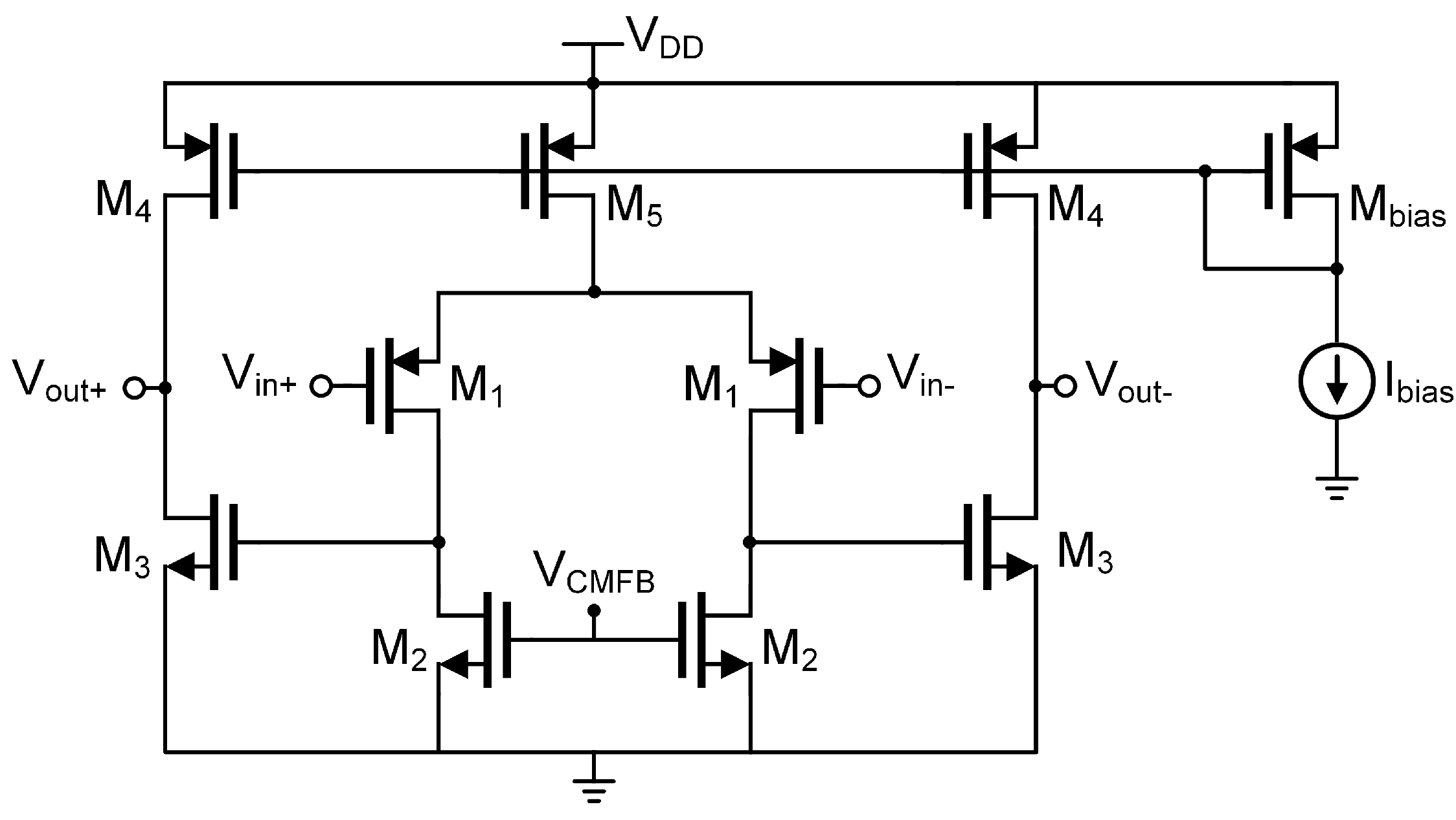
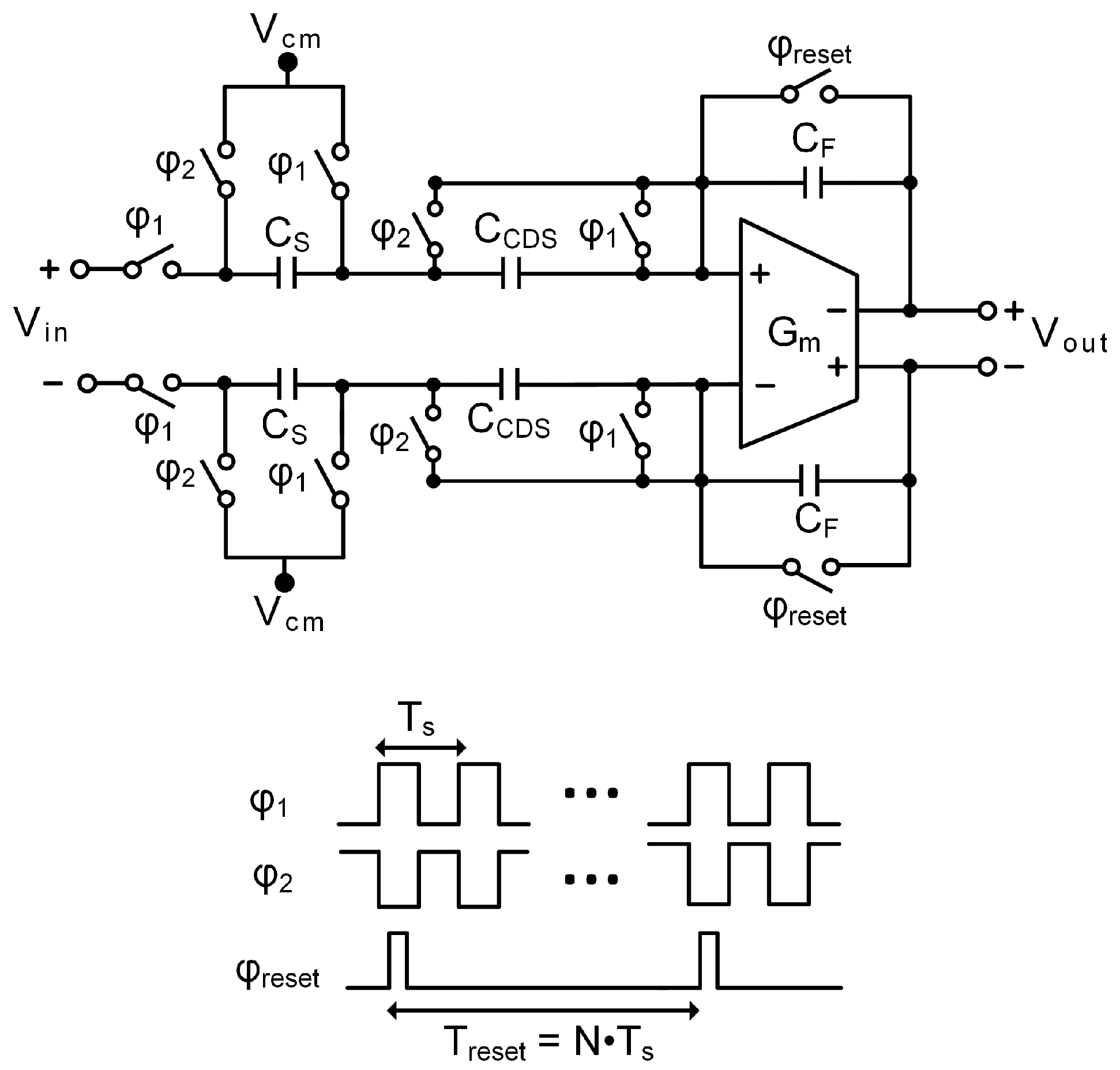
3.4. Switched-Capacitor Integrator with Reset

Traditionally, chopper stabilization requires low-pass filtering after the down-converting chopper modulator in order to filter out the up-converted low-frequency noise and offsets [35,39]. More specifically, a switched-capacitor integrator with reset is able to provide low-pass filtering as its transfer function is mathematically equivalent to the sinc function [40,41,42]. Note that the notches of the sinc function appear at integer multiples of the reset frequency, and that the 3 dB bandwidth of the integrator is approximately equal to 0.44 / T reset [41], where T reset is the period of the reset signal. As displayed in Figure 7, a switched-capacitor integrator [43,44,45] with reset is proposed in lieu of continuous-time passive/active filters or integrators. This integrator is driven by the non-overlapping clock signals ϕ 1 and ϕ 2 with frequency f s = 1 / T s and a reset signal ϕ r e s e t with frequency f r e s e t = 1 / T r e s e t .
A v 2 = f s f r e s e t · C S C F · sin ( π f T r e s e t ) π f T r e s e t
Compared to conventional switched-capacitor amplifiers where sampling and reset share a single clock frequency, the gain of the integrator in this approach is defined not only by the ratio of the sampling and feedback capacitors (i.e., C S and C F ) but also by the ratio of the sampling/reset frequencies (i.e., f s and f reset ). Such a distinction allows for an extra degree of freedom when it comes to setting the gain of the integrator. More precisely, the frequency response of the integrator can be described by Equation (9), which preserves the shaping by the sinc function [40,41,42].
It should be noted that for integration to take place, it is necessary that f s > f reset . The larger the ratio N = f s / f reset , the more samples will be added together before each reset, which translates to a higher gain. In this design, f s = 100 kHz and f reset = 1 kHz . Metal–insulator–metal (MIM) capacitors are selected for C S and C F with a ratio of 0.1, where C S = 0.2 pF and C F = 2 pF . Overall, this implies that, based on Equation (9), the low-frequency gain of the switched-capacitor integrator is 10. In addition, as evident in Figure 7, a correlated double sampling (CDS) technique such as the one in [46,47,48] was implemented to mitigate the effects of finite offsets in the operational transconductance amplifier (OTA) of the integrator. With this approach, the offset of the OTA is sampled in the first phase and then subtracted in the second phase. The value of the correlated double sampling MIM capacitor ( C CDS in Figure 7) is 1 pF. It is also important to mention that the reset takes place when the integrator is in its sampling phase (i.e., ϕ 1 is high to close the sampling switches). A differential folded cascode amplifier [49] is selected as the OTA of choice for this integrator, which is displayed in Figure 8. Node V CMFB is regulated through a common-mode feedback control loop [49]. The simulated low-frequency gain and 3 dB bandwidth of this OTA are 53 dB and 37 kHz, respectively, while the power consumption is 40 μ W from a 1.2 V voltage supply.
Finally, the temperature-to-voltage gain ( A v ) of the proposed two-stage differential temperature sensor circuit can be expressed as in Equation (10).
A v = A v 1 · A v 2 k · g m Q · R o u t · f s f r e s e t · C s C F · sin ( π f T r e s e t ) π f T r e s e t

4. Simulation Results

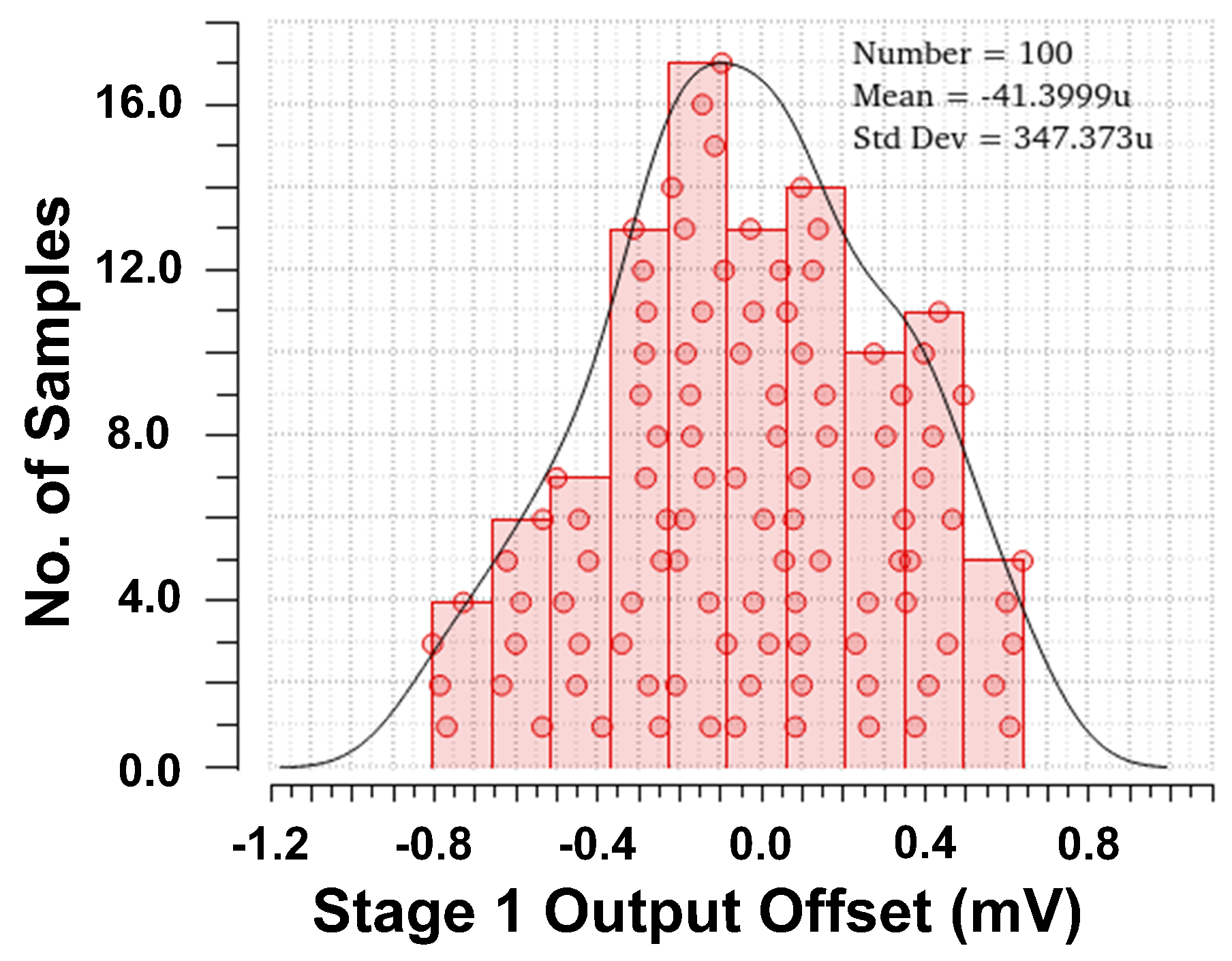
4.1. Evaluation of Stage 1

Schematic simulations were conducted using the Cadence Spectre circuit simulator and foundry-supplied device models for a 65 nm CMOS process. The circuits were designed with a supply voltage of 1.2 V. Figure 9 shows the simulated frequency response of the first stage with chopping enabled, revealing a temperature-to-voltage gain of 9.99 dB with a cutoff frequency at 62.14 kHz, which is in agreement with Equation (2).

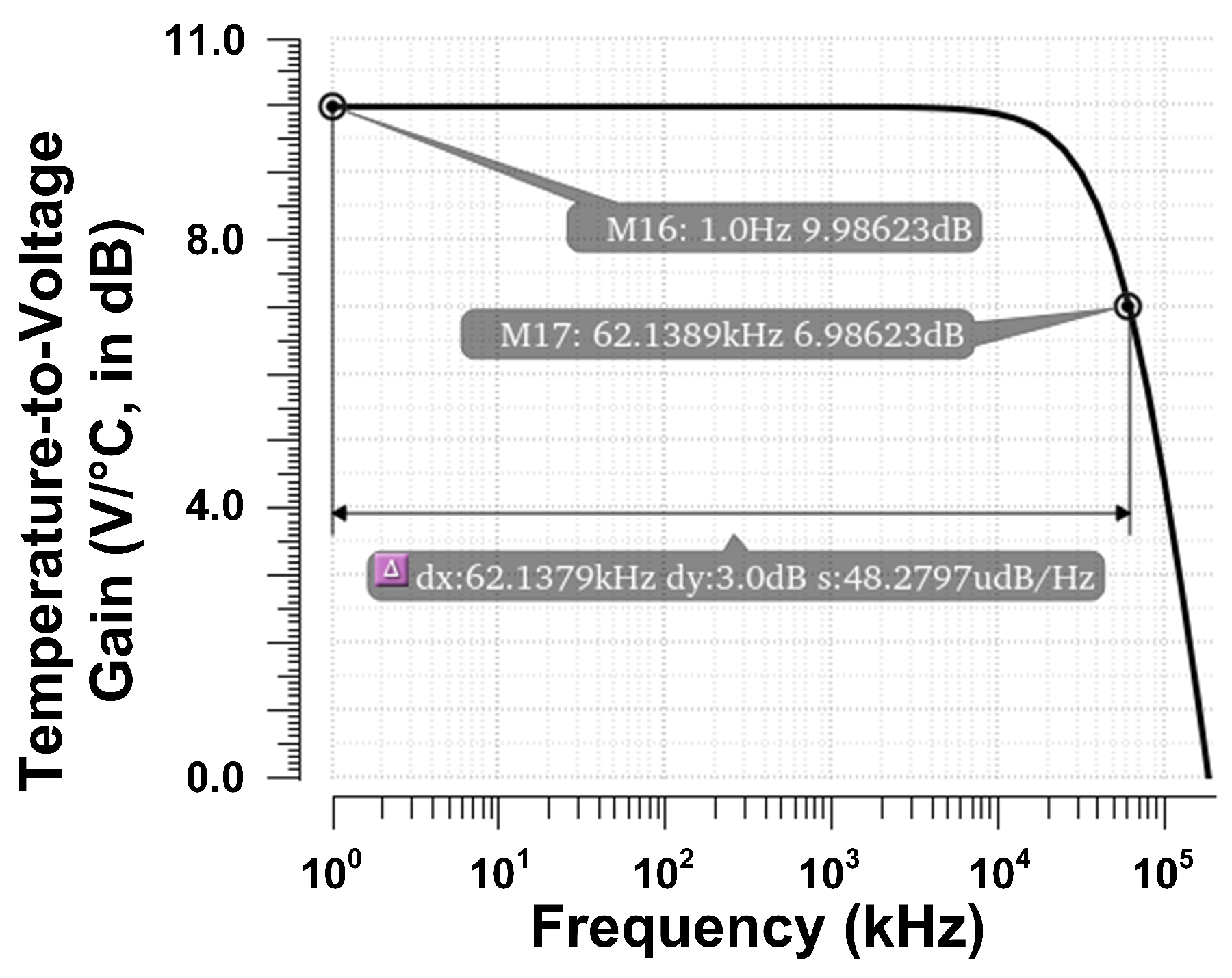
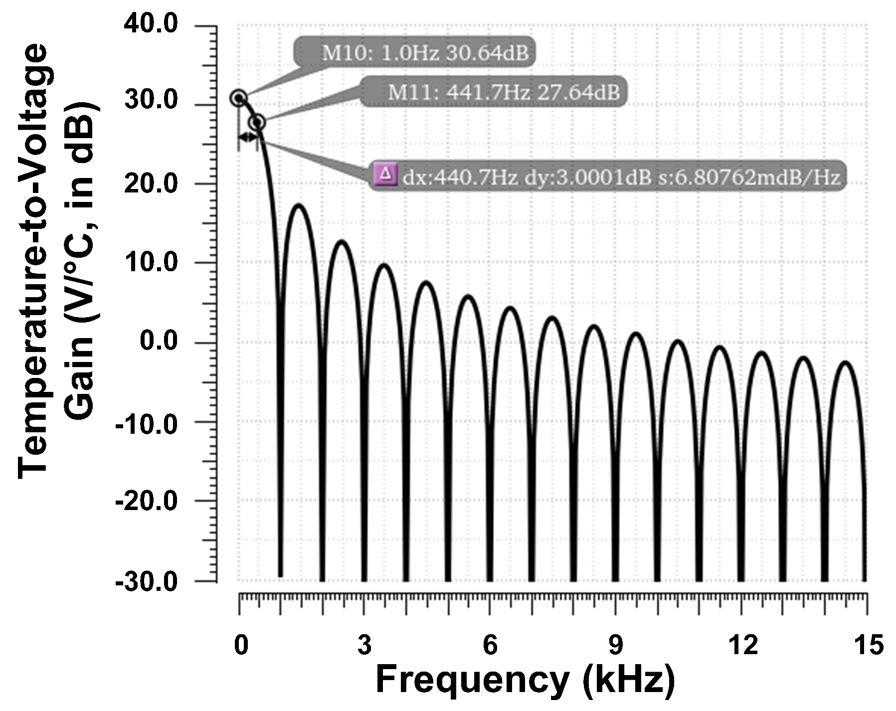
4.2. Frequency Response of the Differential Temperature Sensor

The overall frequency response of the proposed differential temperature sensor is displayed in Figure 10, which was obtained with the help of periodic AC (PAC) simulation. As discussed in Section 3.4, the transfer function of the integrator is equivalent to the sinc function, which is also evident in Figure 10. The simulated temperature-to-voltage gain in the passband is 30.64 dB, which follows Equation (10). The 3 dB frequency of the sensor is 441.7 Hz, which is approximately equal to 0.44 / T reset , as discussed in Section 3.4 [41]. Moreover, as expected, the frequency response is colored by the sinc function of the integrator with notches at integer multiples of the reset frequency ( f reset = 1 kHz ).

4.3. Noise Assessment

The simulation result with chopping (red solid curve) in Figure 11 indicates that the total output-referred noise of the complete temperature sensor circuit is reduced significantly with the help of chopper stabilization, especially compared to the result of the same sensor circuit but without chopping (green dashed curve). Within the 3 dB bandwidth (441.7 Hz) of the proposed differential temperature sensor, the integrated output noise was reduced by a factor of 7.12 thanks to chopping.

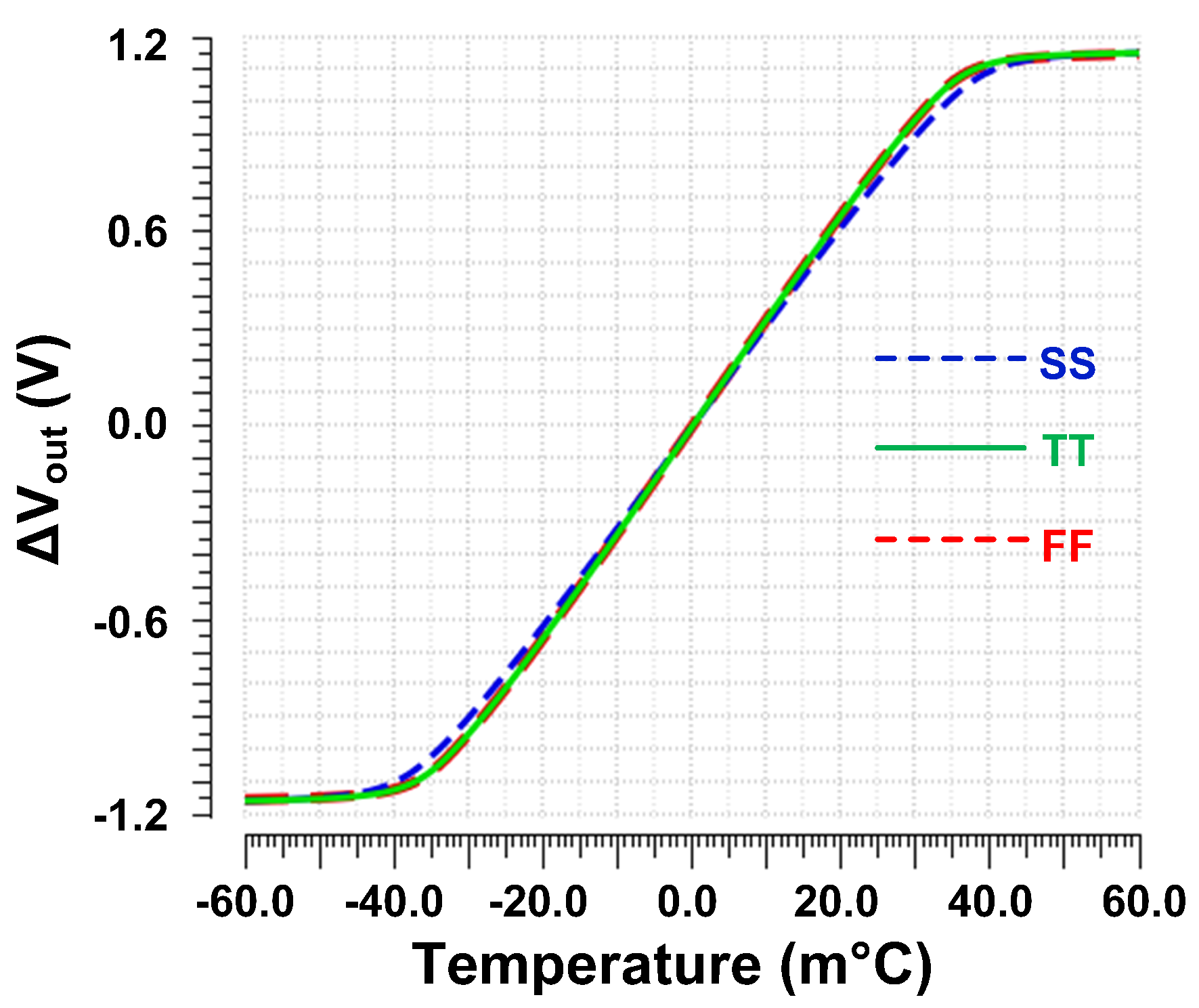
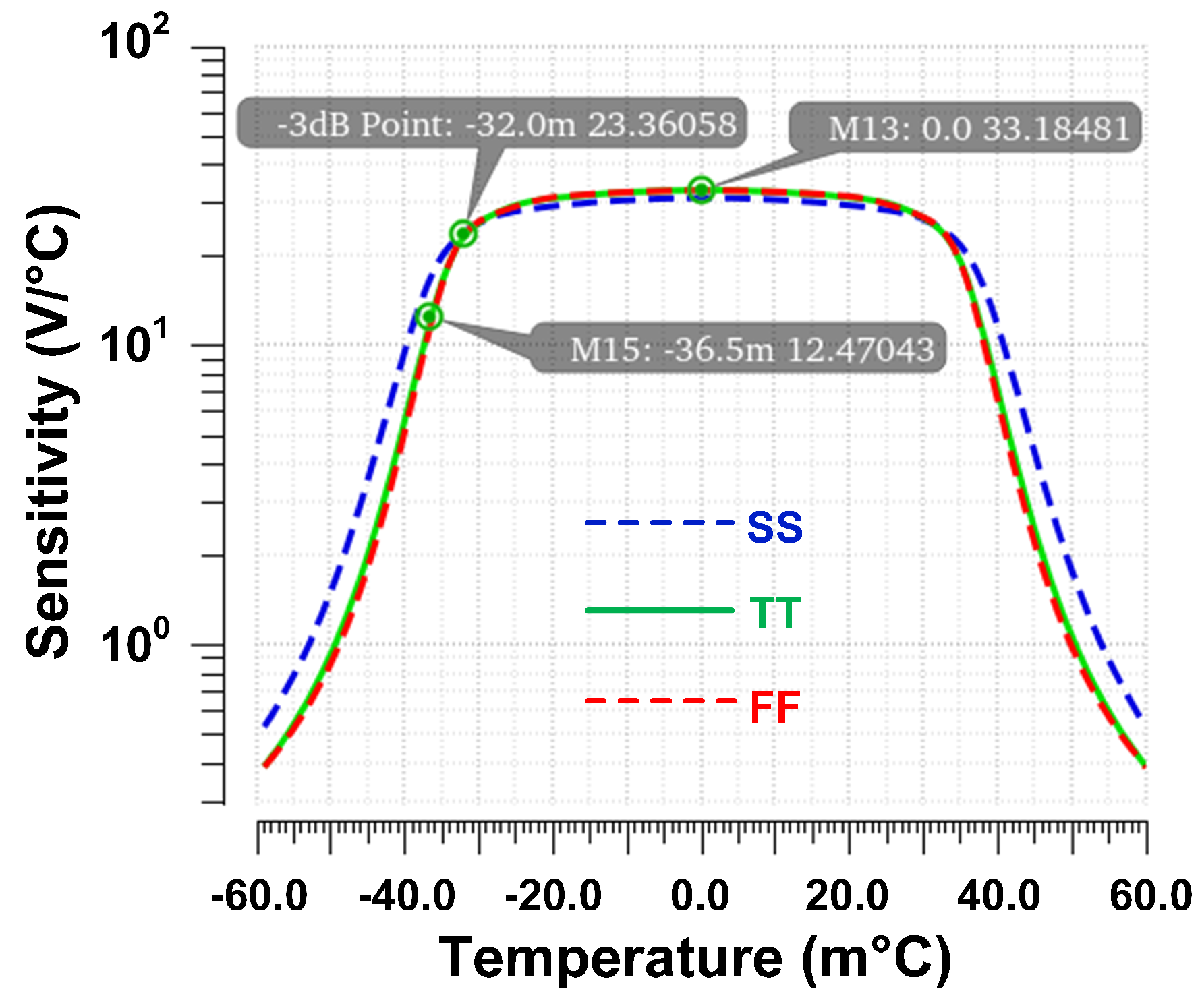
4.4. Sensitivity and Linear Range of the Proposed Differential Temperature Sensor

As can be seen in Figure 12, the output voltage and linear range of the proposed two-stage differential temperature sensor were evaluated under process variations with three process corners: SS (Slow–Slow), TT (Typical–Typical), and FF (Fast–Fast). Here, the linear range is defined as the range of the differential temperature over which the output voltage follows a linear relationship. The correlation between the simulated temperature sensitivity in the TT corner and the line of best fit is 0.995 for a range of ± 36.5 m ° C . The maximum differential temperature measurements error is ± 2.17 m ° C in the range of ± 36.5 m ° C and ± 0.64 m ° C in the range of ± 30 m ° C .
The sensitivity vs. temperature change characteristics in Figure 13 were obtained by taking the derivative of the simulated output voltage curve in Figure 12 with respect to the relative temperature change between the sensing and reference BJTs. In the TT corner, the sensitivity around 0 m ° C is 33.18 V / ° C . The sensitivity in the other process corners (SS and FF) varies from 31.33 V / ° C to 33.13 V / ° C , which decreased by 5.6 % (SS) and increased by + 0.15 % (FF) compared to the TT corner.

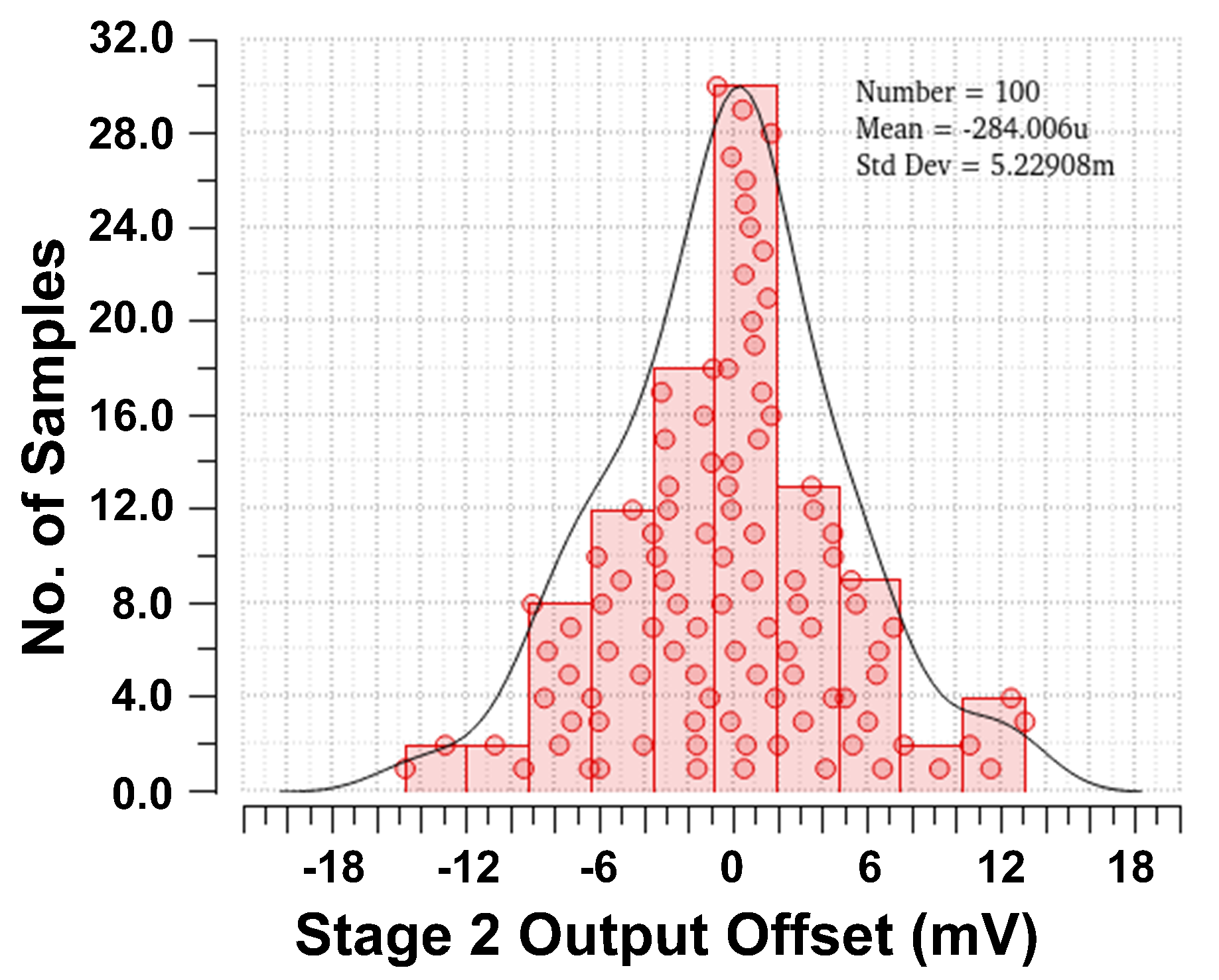
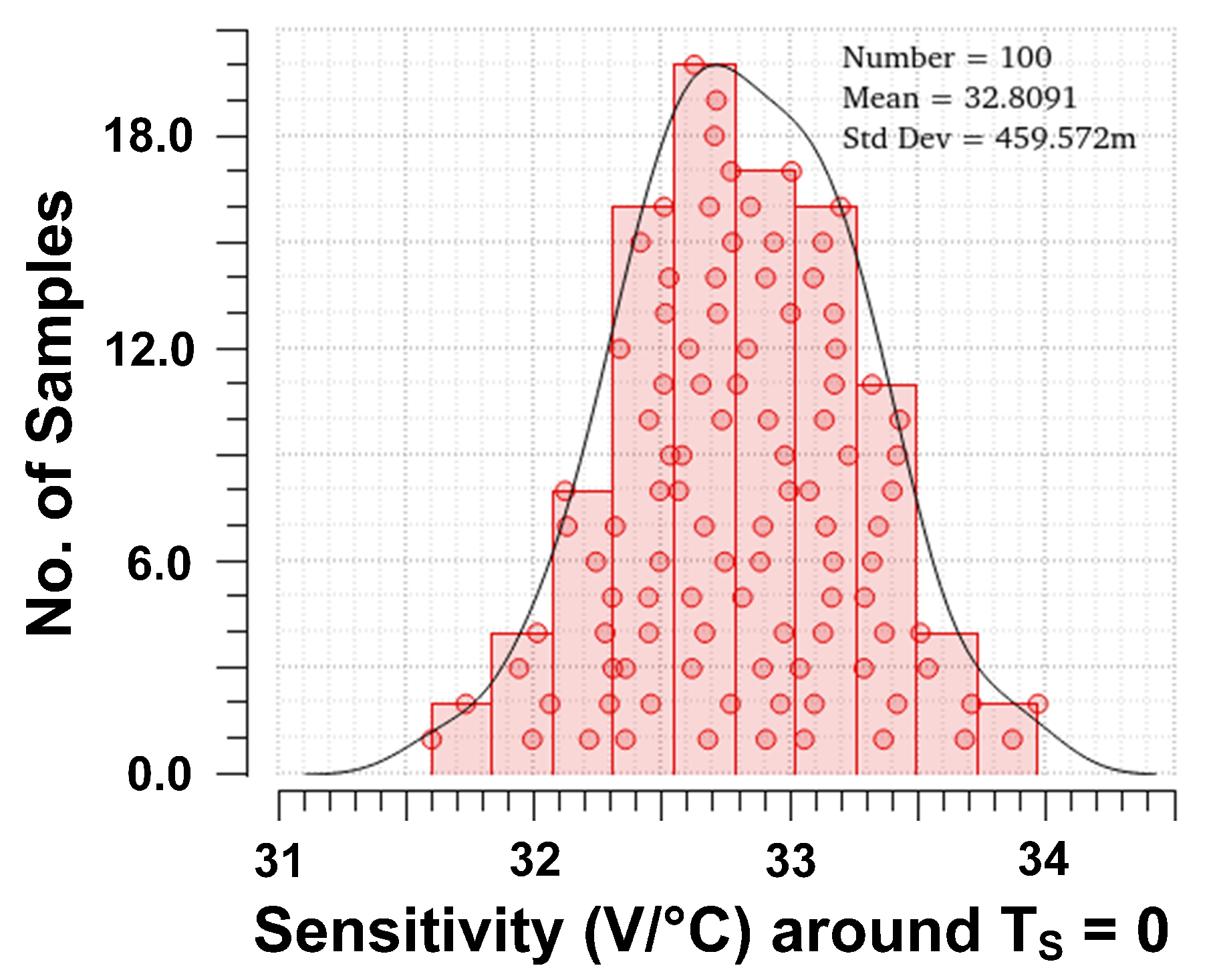
4.5. Monte Carlo Simulations

Monte Carlo simulations were performed to evaluate the effectiveness of the proposed calibration circuit for stage 1 and of the correlated double sampling method for stage 2. The histograms of the output offset voltages of stage 1 and of the complete two-stage differential temperature sensor are displayed in Figure 14 and Figure 15, respectively, which were obtained with transient simulations using statistical device models in the process design kit provided by the foundry. The stage 1 output offset was captured 3 ms after the start of the hold phase. With calibration, the stage 1 output offset after 100 Monte Carlo runs exhibits a mean of 41.4 μ V with a standard deviation of 347.37 μ V . The final two-stage differential temperature sensor output offset has a mean of −284 μ V with a standard deviation of 5.22 mV. Considering that the gain of the two-stage differential temperature sensor is 33.18 V / ° C , the input-referred offset has a mean of −8.6 μ °C with a standard deviation of 158.3 μ °C.
The sensitivity of the complete two-stage differential temperature sensor around T S = 0 was also simulated in the presence of device mismatches. The sensitivity exhibits a mean of 32.8 V / ° C with a standard deviation of 0.459 V / ° C after 100 Monte Carlo simulations with activated calibration. Figure 16 shows the histogram from the simulations.

4.6. Discussion and Comparison with Other Works

Table 1 summarizes the simulated performance specifications of this work in comparison with other on-chip differential temperature sensors for which the simulated sensitivity (in V / ° C ) is reported. Two figures of merit (FoMs) are introduced for comparison between different architectures. In contrast to differential temperature sensors that utilize transimpedance amplifiers [11,12], this work consumes less power while maintaining moderate sensitivity, linear range, and noise. When compared with [9], this work achieves higher sensitivity with similar power consumption. Overall, the simulation results indicate that this work has the highest FoMs compared with other differential temperature sensors for on-chip power monitoring. Therefore, the proposed two-stage differential temperature sensor can provide high performance in a broad range of future application scenarios.

5. Conclusions

A two-stage differential temperature sensor was introduced in this paper alongside its potential utilization in emerging wireless IoT systems for anomaly detection. In the first stage, a cascode structure provides high gain with a significant reduction in power consumption compared to previous high-sensitivity sensors. Furthermore, chopper stabilization was included to mitigate the effects of offsets and low-frequency noise. The discussed design approach involves a chopped cascode transistor technique, which reuses cascode transistors to act as the up-converting chopper modulator without affecting the overall performance of the sensor. This also circumvented a voltage drop in the signal path by avoiding a conventional chopper modulator in series with the cascode transistor. A two-phase calibration circuit was designed to compensate mismatches in the first stage. The second stage of this design consists of a switched-capacitor integrator with correlated double sampling. Due to its transfer function being equivalent to a sinc function, the integrator can provide the necessary low-pass filtering for the up-converted low-frequency noise from chopping while enabling more control of the gain through the use of different reset and sampling frequencies in addition to feedback capacitor values. The proposed design was evaluated with simulations, which indicate a sensitivity of 33.18 V / ° C with a linear range of ± 36.5 m ° C , an integrated (from 1 to 441.7 Hz) output noise of 0.862 mV rms , and an overall power consumption of 0.187 mW . When compared to other differential temperature sensors for on-chip power monitoring, the proposed temperature sensor topology shows a notable performance improvement when considering a figure of merit that takes into account sensitivity, linear range, noise, and power consumption.

Author Contributions

Conceptualization, J.Y., T.G., M.Y., R.D., A.M., M.Z., F.R., A.S., Y.F. and M.O.; validation, J.Y., T.G. and M.O.; formal analysis, J.Y., T.G., M.Y. and M.O.; investigation, J.Y. and T.G.; simulation, J.Y. and T.G.; resources, F.R., A.S., Y.F. and M.O.; data curation, J.Y. and T.G.; writing—original draft preparation, J.Y., T.G. and M.O.; writing—review and editing, J.Y., T.G., M.Y., R.D., A.M., M.Z., F.R., A.S., Y.F. and M.O.; visualization, J.Y. and T.G.; supervision, F.R., A.S., Y.F. and M.O.; project administration, M.O.; funding acquisition, F.R., A.S., Y.F. and M.O. All authors have read and agreed to the published version of the manuscript.

Funding

This work was supported in part by the National Science Foundation (NSF) under grants 2146754, 2225368, CCF-2218845, ECCS-2229472, ECCS-2329013, CNS-2212010, and CHEST IUCRC 24_24; in part by the funds from OUSD(R&E), NIST; in part by the Industry Partners as Specified in the Resilient and Intelligent NextG Systems (RINGS) Program; in part by the Office of Naval Research under Grant N00014-23-1-2221; in part by DARPA D23AP00173; and in part by the Air Force Office of Scientific Research under Grant FA9550-23-1-0261.

Data Availability Statement

Data are contained within the article.

Acknowledgments

The authors would like to thank Minghan Liu, Yunfan Gao, Diptashree Das, and Safaa Abdelfattah for valuable discussions and suggestions. The authors would also like to thank the anonymous reviewers for their insightful suggestions and comments, which helped to improve the quality of the paper.

Conflicts of Interest

Author M.Y. is employed by the company Analog Devices Inc., and was previously affiliated with Northeastern University. The remaining authors declare that the research was conducted in the absence of any commercial or financial relationships that could be construed as a potential conflict of interest.

References

  1. Altet, J.; Rubio, A.; Schaub, E.; Dilhaire, S.; Claeys, W. Thermal coupling in integrated circuits: Application to thermal testing. IEEE J. Solid-State Circuits 2001, 36, 81–91. [Google Scholar] [CrossRef]
  2. Altet, J.; Claeys, W.; Dilhaire, S.; Rubio, A. Dynamic surface temperature measurements in ICs. Proc. IEEE 2006, 94, 1519–1533. [Google Scholar] [CrossRef]
  3. Nenadovic, N.; Mijalkovic, S.; Nanver, L.K.; Vandamme, L.K.; d’Alessandro, V.; Schellevis, H.; Slotboom, J.W. Extraction and modeling of self-heating and mutual thermal coupling impedance of bipolar transistors. IEEE J. Solid-State Circuits 2004, 39, 1764–1772. [Google Scholar] [CrossRef]
  4. Mattisson, S.; Hagberg, H.; Andreani, P. Sensitivity degradation in a tri-band GSM BiCMOS direct-conversion receiver caused by transient substrate heating. IEEE J. Solid-State Circuits 2008, 43, 486–496. [Google Scholar] [CrossRef]
  5. Lee, S.S.; Allstot, D.J. Electrothermal simulation of integrated circuits. IEEE J. Solid-State Circuits 1993, 28, 1283–1293. [Google Scholar] [CrossRef]
  6. Mateo, D.; Aragones, X.; Barajas, E.; Martínez, S.; Gisbert, X.; Altet, J. High Sensitivity Temperature Measurements to Track and Compensate Aging Effects on CMOS Amplifiers. IEEE Trans. Device Mater. Reliab. 2024, 25, 11–16. [Google Scholar] [CrossRef]
  7. Abdallah, L.; Stratigopoulos, H.G.; Mir, S.; Altet, J. Defect-oriented non-intrusive RF test using on-chip temperature sensors. In Proceedings of the IEEE 31st VLSI Test Symposium (VTS), Berkeley, CA, USA, 29 April–2 May 2013. [Google Scholar] [CrossRef]
  8. Aragones, X.; Mateo, D.; González, J.; Vidal, E.; Gómez, D.; Martineau, B.; Altet, J. DC temperature measurements to characterize the central frequency and 3 dB bandwidth in mmW power amplifiers. IEEE Microw. Wirel. Components Lett. 2015, 25, 745–747. [Google Scholar] [CrossRef]
  9. Altet, J.; Mateo, D.; Gómez, D.; González Jiménez, J.L.; Martineau, B.; Siligaris, A.; Aragones, X. Temperature Sensors to Measure the Central Frequency and 3 dB Bandwidth in mmW Power Amplifiers. IEEE Microw. Wirel. Components Lett. 2014, 24, 272–274. [Google Scholar] [CrossRef]
  10. Onabajo, M.; Altet, J.; Aldrete-Vidrio, E.; Mateo, D.; Silva-Martinez, J. Electrothermal Design Procedure to Observe RF Circuit Power and Linearity Characteristics With a Homodyne Differential Temperature Sensor. IEEE Trans. Circuits Syst. I Reg. Pap. 2011, 58, 458–469. [Google Scholar] [CrossRef]
  11. Wei, H.; Yan, M.; Onabajo, M. Noise reduction via chopper stabilization of fully differential temperature sensors for hardware security applications. In Proceedings of the IEEE 14th Dallas Circuits and Systems Conference (DCAS), Dallas, TX, USA, 15–16 November 2020. [Google Scholar] [CrossRef]
  12. Yan, M.; Wei, H.; Onabajo, M. On-Chip Thermal Profiling to Detect Malicious Activity: System-Level Concepts and Design of Key Building Blocks. IEEE Trans. Very Large Scale Integr. VLSI Syst. 2021, 29, 530–543. [Google Scholar] [CrossRef]
  13. Yan, M.; Gourousis, T.; Onabajo, M. On-Chip Power Monitoring: Leveraging High-Sensitivity Differential Temperature Sensors with Chopper Stabilization and Offset Calibration. IEEE Trans. Instrum. Meas. 2024, 73, 2002404. [Google Scholar] [CrossRef]
  14. Aprile, A.; Moisello, E.; Bonizzoni, E.; Malcovati, P. Performance comparison of BJT and MOS devices as temperature sensing elements. In Proceedings of the IEEE 29th International Conference on Electronics, Circuits and Systems (ICECS), Glasgow, UK, 24–26 October 2022. [Google Scholar] [CrossRef]
  15. Altet, J.; Barajas, E.; Mateo, D.; Billong, A.; Aragones, X.; Perpiñà, X.; Reverter, F. BPF-based thermal sensor circuit for on-chip testing of RF circuits. Sensors 2021, 21, 805. [Google Scholar] [CrossRef] [PubMed]
  16. Reverter, F.; Altet, J. On-chip thermal testing using MOSFETs in weak inversion. IEEE Trans. Instrum. Meas. 2014, 64, 524–532. [Google Scholar] [CrossRef]
  17. Sengupta, K.; Dasgupta, K.; Bowers, S.M.; Hajimiri, A. On-chip sensing and actuation methods for integrated self-healing mm-wave CMOS power amplifier. In Proceedings of the IEEE/MTT-S International Microwave Symposium Digest, Montreal, QC, Canada, 17–22 June 2012. [Google Scholar] [CrossRef]
  18. Nowroz, A.N.; Hu, K.; Koushanfar, F.; Reda, S. Novel techniques for high-sensitivity hardware Trojan detection using thermal and power maps. IEEE Trans. Comput. Aided Des. Integr. Circuits Syst. 2014, 33, 1792–1805. [Google Scholar] [CrossRef]
  19. Cao, Y.; Chang, C.H.; Chen, S. A cluster-based distributed active current sensing circuit for hardware Trojan detection. IEEE Trans. Inf. Forensics Secur. 2014, 9, 2220–2231. [Google Scholar] [CrossRef]
  20. Gourousis, T.; Zhang, Z.; Yan, M.; Zhang, M.; Mittal, A.; Shrivastava, A.; Restuccia, F.; Fei, Y.; Onabajo, M. Identification of Stealthy Hardware Trojans through On-Chip Temperature Sensing and an Autoencoder-Based Machine Learning Algorithm. In Proceedings of the IEEE 66st International Midwest Symposium on Circuits and Systems (MWSCAS), Tempe, AZ, USA, 6–9 August 2023. [Google Scholar] [CrossRef]
  21. Mittal, A.; Zhang, M.; Gourousis, T.; Zhang, Z.; Fei, Y.; Onabajo, M.; Restuccia, F.; Shrivastava, A. Sub-6 GHz energy detection-based fast on-chip analog spectrum sensing with learning-driven signal classification. IEEE Internet Things J. 2024, 11, 2503–25046. [Google Scholar] [CrossRef]
  22. Ba, A.; Liu, Y.H.; van den Heuvel, J.; Mateman, P.; Büsze, B.; Dijkhuis, J.; Bachmann, C.; Dolmans, G.; Philips, K.; De Groot, H. A 1.3 nJ/b IEEE 802.11ah fully-digital polar transmitter for IoT applications. IEEE J. Solid-State Circuits 2016, 51, 3103–3113. [Google Scholar] [CrossRef]
  23. Liu, D.; Ni, X.; Zhou, R.; Rhee, W.; Wang, Z. A 0.42-mW 1-Mb/s 3-to-4-GHz transceiver in 0.18-μm CMOS with flexible efficiency, bandwidth, and distance control for IoT applications. IEEE J. Solid-State Circuits 2017, 52, 1479–1494. [Google Scholar] [CrossRef]
  24. Tang, K.; Yang, C.; Guo, Y.; Wang, N.; Zhu, Y.; Zhang, Y.; Ng, E.J.; Lee, J.E.Y.; Fang, Z.; Wang, W.; et al. A 107 pJ/b TX 260 pJ/b RX ultralow-power MEMS-based transceiver with wake-up in ISM-bands for IoT applications. IEEE J. Solid-State Circuits 2022, 58, 1337–1349. [Google Scholar] [CrossRef]
  25. Yi, H.; Yu, W.H.; Mak, P.I.; Yin, J.; Martins, R.P. A 0.18-V 382-μW Bluetooth Low-Energy receiver front-end with 1.33-nW sleep power for energy-harvesting applications in 28-nm CMOS. IEEE J. Solid-State Circuits 2018, 53, 1618–1627. [Google Scholar] [CrossRef]
  26. Yan, M.; Wei, H.; Onabajo, M. Modeling of thermal coupling and temperature sensor circuit design considerations for hardware Trojan detection. In Proceedings of the IEEE 61st International Midwest Symposium on Circuits and Systems (MWSCAS), Windsor, ON, Canada, 5–8 August 2018. [Google Scholar] [CrossRef]
  27. Osipov, D.; Paul, S. Temperature-Compensated β -Multiplier Current Reference Circuit. IEEE Trans. Circuits Syst. II Express Briefs 2017, 64, 1162–1166. [Google Scholar] [CrossRef]
  28. Ivanov, V.; Brederlow, R.; Gerber, J. An ultra low power bandgap operational at supply from 0.75 V. IEEE J. Solid-State Circuits 2012, 47, 1515–1523. [Google Scholar] [CrossRef]
  29. Ji, Y.; Lee, J.; Kim, B.; Park, H.J.; Sim, J.Y. A 192-pW Voltage Reference Generating Bandgap—Vth With Process and Temperature Dependence Compensation. IEEE J. Solid-State Circuits 2019, 54, 3281–3291. [Google Scholar] [CrossRef]
  30. Vita, G.D. A Sub 1-V, 10 ppm/℃, Nanopower Voltage Reference Generator. IEEE J. Solid-State Circuits 2007, 42, 1536–1542. [Google Scholar] [CrossRef]
  31. Fiori, F.; Crovetti, P.S. A new compact temperature-compensated CMOS current reference. IEEE Trans. Circuits Syst. II Express Briefs 2005, 52, 724–728. [Google Scholar] [CrossRef]
  32. Lee, J.; Cho, S. A 1.4-μW 24.9-ppm/°C current reference with process-insensitive temperature compensation in 0.18-μm CMOS. IEEE J. Solid-State Circuits 2012, 47, 2527–2533. [Google Scholar] [CrossRef]
  33. Razavi, B. Design of Analog CMOS Integrated Circuits, 2nd ed.; McGraw-Hill Education: New York, NY, USA, 2016; 254p. [Google Scholar]
  34. Gray, P.R.; Hurst, P.J.; Lewis, S.H.; Meyer, R.G. Analysis and Design of Analog Integrated Circuits, 5th ed.; John Wiley & Sons: Hoboken, NJ, USA, 2009; 745p. [Google Scholar]
  35. Enz, C.; Temes, G. Circuit techniques for reducing the effects of op-amp imperfections: Autozeroing, correlated double sampling, and chopper stabilization. Proc. IEEE 1996, 84, 1584–1614. [Google Scholar] [CrossRef]
  36. Oh, W.; Bakkaloglu, B.; Wang, C.; Hoon, S.K. A CMOS low noise, chopper stabilized low-dropout regulator with current-mode feedback error amplifier. IEEE Trans. Circuits Syst. I Regul. Pap. 2008, 55, 3006–3015. [Google Scholar] [CrossRef]
  37. Wu, J.; Law, M.K.; Mak, P.I.; Martins, R.P. A 2-μW, 45-nV/Hz Readout Front End With Multiple-Chopping Active-High-Pass Ripple Reduction Loop and Pseudofeedback DC Servo Loop. IEEE Trans. Circuits Syst. II Express Briefs 2015, 63, 351–355. [Google Scholar] [CrossRef]
  38. Yang, T.; Lu, J.; Poore, N.; Holleman, J. A current-reuse complementary-input chopper-stabilized amplifier for neural recording. In Proceedings of the IEEE 12th International New Circuits and Systems Conference (NEWCAS), Trois-Rivieres, QC, Canada, 22–25 June 2014. [Google Scholar] [CrossRef]
  39. Enz, C.C.; Vittoz, E.A.; Krummenacher, F. A CMOS chopper amplifier. IEEE J. Solid-State Circuits 1987, 22, 335–342. [Google Scholar] [CrossRef]
  40. Carusone, T.C.; Johns, D.A.; Martin, K.W. Analog Integrated Circuit Design; John Wiley & Sons: Hoboken, NJ, USA, 2011. [Google Scholar]
  41. Xu, G.; Yuan, J. Performance analysis of general charge sampling. IEEE Trans. Circuits Syst. II Express Briefs 2005, 52, 107–111. [Google Scholar] [CrossRef]
  42. Jiang, W.; Zhu, Y.; Chan, C.H.; Murmann, B.; Martins, R.P. A 7-bit 2 GS/s time-interleaved SAR ADC with timing skew calibration based on current integrating sampler. IEEE Trans. Circuits Syst. I Regul. Pap. 2020, 68, 557–568. [Google Scholar] [CrossRef]
  43. Gregorian, R.; Martin, K.W.; Temes, G.C. Switched-capacitor circuit design. Proc. IEEE 1983, 71, 941–966. [Google Scholar] [CrossRef]
  44. Liu, J.; Allstot, D.J. A Chopper-Stabilized Switched-Capacitor Front-End for Peripheral Nervous System Recording. IEEE Trans. Circuits Syst. I Regul. Pap. 2023, 70, 3065–3074. [Google Scholar] [CrossRef]
  45. Liu, J.; Walker, R.M. A compact, low-noise, chopped front-end for peripheral nerve recording in 180 nm CMOS. In Proceedings of the 2018 IEEE Biomedical Circuits and Systems Conference (BioCAS), Cleveland, OH, USA, 17–19 October 2018. [Google Scholar] [CrossRef]
  46. Oliaei, O. Noise analysis of correlated double sampling SC integrators with a hold capacitor. IEEE Trans. Circuits Syst. I Fundam. Theory Appl. 2003, 50, 1198–1202. [Google Scholar] [CrossRef]
  47. Chen, H.L.; Chen, P.S.; Chiang, J.S. A low-offset low-noise sigma-delta modulator with pseudorandom chopper-stabilization technique. IEEE Trans. Circuits Syst. I Regul. Pap. 2009, 56, 2533–2543. [Google Scholar] [CrossRef]
  48. Belloni, M.; Bonizzoni, E.; Fornasari, A.; Maloberti, F. A micropower chopper—CDS operational amplifier. IEEE J. Solid-State Circuits 2010, 45, 2521–2529. [Google Scholar] [CrossRef]
  49. Mallya, S.; Nevin, J.H. Design procedures for a fully differential folded-cascode CMOS operational amplifier. IEEE J. Solid-State Circuits 2002, 24, 1737–1740. [Google Scholar] [CrossRef]
Figure 1. Block diagram of the proposed two-stage differential temperature sensor.
Electronics 14 02381 g001
Figure 2. IoT system with a transceiver at the node that contains on-chip temperature sensing and spectrum sensing circuits to communicate with an edge device that executes machine learning-based anomaly detection.
Electronics 14 02381 g002
Figure 3. Envisioned sensing and wireless transmission of temperature data.
Electronics 14 02381 g003
Figure 4. (a) Temperature-sensing BJT-based cascode differential amplifier with chopped cascode transistors, (b) activation of M 3 B transistors, and (c) activation of M 3 A transistors.
Electronics 14 02381 g004
Figure 5. Calibration circuit for the compensation of electrical mismatches and on-chip thermal gradients prior to measurements.
Electronics 14 02381 g005
Figure 6. Two-stage amplifier in the calibration circuit.
Electronics 14 02381 g006
Figure 7. Switched-capacitor integrator with reset and correlated double sampling.
Electronics 14 02381 g007
Figure 8. Folded-cascode amplifier used as OTA in the switched-capacitor integrator.
Electronics 14 02381 g008
Figure 9. Simulated temperature-to-voltage gain ( V o u t / T s ) of stage 1.
Electronics 14 02381 g009
Figure 10. Simulated frequency response of the two-stage temperature sensor.
Electronics 14 02381 g010
Figure 11. Simulated output noise of the two-stage differential temperature sensor with chopping (red solid curve) and without chopping (green dashed curve).
Electronics 14 02381 g011
Figure 12. Simulated linear range of the two-stage differential temperature sensor in the presence of process variations.
Electronics 14 02381 g012
Figure 13. Sensitivity of the two-stage differential sensor vs. temperature change in the presence of process variations.
Electronics 14 02381 g013
Figure 14. Histogram of the output offset voltage of stage 1 after Monte Carlo simulations.
Electronics 14 02381 g014
Figure 15. Histogram of the output offset voltage of the two-stage differential temperature sensor after Monte Carlo simulations.
Electronics 14 02381 g015
Figure 16. Histogram of the sensitivity (around T S = 0) of the two-stage differential temperature sensor after Monte Carlo simulations.
Electronics 14 02381 g016
Table 1. Comparison with other differential temperature sensors for which simulation results are reported.
ParameterThis Work[9][11][12]
Technology (nm)6565130130
Sensitivity ( V / ° C )33.180.62.09840
Linear Range ( m ° C )±36.5±600±210±1
Integrated Output Noise [1– f c Hz] ( mV rms )0.862n/a0.3860
Power Consumption (mW)0.1870.13681.081.452
FoM 1  (1/mW)7513n/a10699.64
FoM 2  (V/mW)6.4762.6320.4060.579
f c is the cutoff frequency of the temperature sensors. n/a: not reported or not applicable. FoM 1 = Sensitivity × Linear Range Power × Integrated Output Noise (1/mW); FoM 2 = Sensitivity × Linear Range Power (V/mW).
Disclaimer/Publisher’s Note: The statements, opinions and data contained in all publications are solely those of the individual author(s) and contributor(s) and not of MDPI and/or the editor(s). MDPI and/or the editor(s) disclaim responsibility for any injury to people or property resulting from any ideas, methods, instructions or products referred to in the content.

