Abstract
This paper presents a class-D outphasing power amplifier (PA) that incorporates a non-isolating balun combiner employing a 180° phase shift. Both isolating and non-isolating outphasing combiners are analyzed for signal restoration and combining efficiency. The proposed non-isolating balun combiner employing the 180° phase shift was experimentally evaluated and compared with a commercial isolating Wilkinson combiner. When two constant-envelope signals derived from a 10 MHz long-term evolution (LTE) signal are applied to the inputs of the outphasing combiners, both combiners demonstrate successful signal reconstruction. The measured adjacent channel leakage ratios (ACLRs) are −47 dBc for the Wilkinson combiner and −46 dBc for the proposed balun combiner. At 6 dB power back-off (PBO), the proposed balun combiner achieves a combining efficiency of 85.1%, representing an improvement of nearly 60% over the Wilkinson combiner. With a center frequency of 650 MHz, targeting 5G FR1 applications, a class-D outphasing PA was designed in a 28 nm CMOS process using the measured S-parameter data from both outphasing combiners. Simulation results show that the class-D outphasing PA incorporating the proposed balun combiner achieves a peak drain efficiency (DE) of 82.9% with an output power of 17.7 dBm. At 6 dB PBO, the DE reaches 61%, which is approximately 37% higher than that of the outphasing PA using the Wilkinson combiner. Moreover, the designed outphasing PA supports broadband operation over the 360–860 MHz range.
1. Introduction
As digital modulation schemes in wireless communication systems continue to evolve, the linearity requirements for power amplifiers (PAs) in transmitters have become increasingly stringent. These demanding linearity specifications often result in reduced transmitter efficiency, thereby prompting the need for alternative approaches to enhance efficiency. One such approach is the LINC (Linear Amplification with Nonlinear Components) system, also known as the outphasing technique, which has been proposed to address this challenge [1,2]. The key advantage of the outphasing system is its ability to maintain high efficiency by reducing the DC current as output power decreases, without degrading signal linearity.
The LINC system employs a signal component separator (SCS) to transform an input variable-envelope signal into two constant-envelope signals, as illustrated in Figure 1a. Specifically, an amplitude- and phase-modulated RF signal, , can be decomposed into two constant-amplitude, phase-modulated signals according to the following expressions:
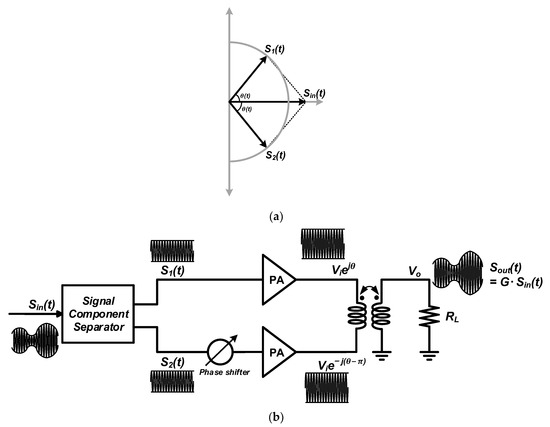 where, represents the angular frequency, is the instantaneous amplitude of the signal , denotes the maximum value of and is the phase of the baseband signal. refers to the additional phase-modulation angle associated with the amplitude of , also known as the outphasing angle. The two outphased constant-envelope signals, and , are individually amplified using highly efficient nonlinear PAs and subsequently combined via an outphasing combiner. Accurate signal reconstruction through the outphasing combiner requires that the amplitude of the combined signal satisfy the condition specified in Equation (3). Consequently, the summation property is achieved when the output signal amplitude is proportional to [3].
Figure 1.
Outphasing principle and outphasing PA architecture: (a) outphasing vector diagram; (b) outphasing PA architecture with a proposed balun combiner employing a 180° phase shift.
In an outphasing system, the outphasing combiner plays a critical role in determining both efficiency and linearity. This combiner can be implemented using either an isolating or a non-isolating topology. An isolating combiner, such as the Wilkinson combiner [4] provides good linearity due to the isolation it offers between the two PAs. However, it maintains a constant supply current regardless of variations in the amplitude of the signal, which results in lower average efficiency. Conversely, a non-isolating combiner introduces time-varying impedances to the PAs due to mutual interaction between the two PAs. Although practical PAs do not behave as ideal voltage sources, the output voltage characteristics of switching PAs and saturated class-B/C PAs still allow for some efficiency enhancement under such conditions [5]. Representative non-isolating combiners include a quarter-wavelength transmission line-based combiner and a series transformer-based combiner [3,5,6,7,8,9,10,11,12,13,14,15]. To enhance power back-off (PBO) efficiency, Chireix compensation has been applied to these combiners in previous studies [5,6,7,8,9,10,11]. However, in practical scenarios involving non-ideal voltage sources with nonzero output impedance, the introduction of Chireix compensation elements can cause linearity degradation [16]. As a result, digital predistortion (DPD) techniques are commonly employed to mitigate such distortion, although they increase overall system complexity [5,8,9,10,11].
This paper presents a non-isolating balun outphasing combiner employing a 180° phase shift for a class-D PA. Class-D and class-F PAs, which behave more like voltage sources and exhibit reduced sensitivity to load impedance variations, are preferred for achieving good linearity in outphasing systems [17,18,19]. Although class-F PAs provide high linearity, their bulky resonant circuits make them less suitable for integration. In contrast, class-D PAs, which are more amenable to on-chip implementation, offer a more practical solution [3,12,13,14,15]. Figure 1b illustrates the structure of the proposed balun combiner with a switching PA for outphasing operation. This balun combiner is based on a conventional balun structure but includes a 180° phase shifter. The phase shifter enables the realization of the summation property by canceling out out-of-phase signal components, thereby allowing only in-phase components to be combined. As discussed earlier, quarter-wavelength transmission line-based combiners and series transformer-based combiners are commonly employed as non-isolating combiners. However, in practical implementations, both types tend to be structurally bulky and complex. To address this issue, this study proposes a class-D outphasing PA incorporating a balun combiner with a 180° phase shift that offers compact size, broadband capability and both high efficiency and linearity, making it a promising solution for outphasing applications.
This paper is organized as follows. Section 2 presents an analysis of both isolating and non-isolating combiners. In Section 3, the measurement results of the commercial Wilkinson combiner and the proposed balun combiner with the 180 phase shift are compared. Section 4 introduces a class-D outphasing PA based on the measured S-parameter data of the combiners. Finally, Section 5 provides concluding remarks.
2. Analysis of the Isolating and Non-Isolating Combiners
In an outphasing system, achieving a high level of power efficiency critically depends on the design of the output combiner. Figure 2 illustrates ideal configurations of both isolating and non-isolating combiners. Specifically, Figure 2a depicts an isolating Wilkinson combiner, while Figure 2b,c show two representative non-isolating combiners: the quarter-wavelength transmission line-based combiner and the series transformer-based combiner. Figure 2d presents the proposed balun combiner employing the 180° phase shift. The output signals of each switching PA are modeled as voltage sources, defined as and .
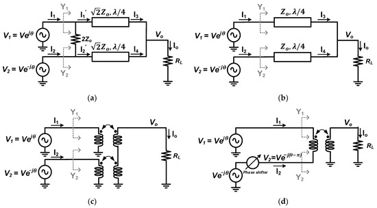
Figure 2.
Ideal outphasing combiner; (a) Wilkinson combiner; (b) quarter-wavelength transmission line-based combiner; (c) series transformer-based combiner; (d) proposed balun combiner with the 180° phase shift.
First, the outphasing operation for the Wilkinson combiner is analyzed. Through the quarter-wavelength transmission lines, voltage and current are reciprocally converted [20]. Thus, the following relations hold:
Here, denotes the characteristic impedance. and represent the currents flowing before each quarter-wavelength transmission line, while and are the currents after passing through the lines. The relations for the output current and output voltage can be derived from Equation (5):
Since the output voltage is proportional to , it can be confirmed that the summation property is satisfied. The input current along with its magnitude are expressed as:
It can be observed that remains constant regardless of . The input admittance derived from Equation (9) is given by:
In an isolating combiner, the admittance presented at each PA’s output remains constant, as shown in Equation (10). Let and denote the two available RF input powers to the combiner, and let be the RF power delivered to the load at the output of the combiner. Based on the above relationships, the power expressions are as follows:
The isolating combiner supplies constant input power regardless of , while the output power varies proportionally with . The difference in power, not delivered to the load, is dissipated through the isolation resistor. Since the output power is proportional to , the output power at 6 dB PBO represents the point where , which corresponds to . The combining efficiency , based on Equations (11) through (13), is defined as:
From Equation (14), it can be observed that in an isolating combiner, the combining efficiency at 6 dB PBO is ideally 25%.
In the quarter-wavelength transmission line-based combiner shown in Figure 2b, the output current and output voltage are given by:
It can be confirmed from Equation (16) that the summation property is satisfied. The resulting input current is expressed as:
Unlike in an isolating combiner, the magnitude is proportional to . This results in reduced power dissipation in the out-of-phase components, thereby enhancing PBO combining efficiency. The corresponding input admittance is given by:
In a non-isolating combiner, the admittance presented at each PA’s output varies with due to load modulation. Thus, , and are expressed as follows:
The combining efficiency , derived from Equations (19)–(21) is given by:
Therefore, in a non-isolating combiner, load modulation reduces the power required to generate the combined out-of-phase signal, thereby enhancing PBO combining efficiency. In the case of a lossless combiner, as shown in Equation (22), the combining efficiency remains 100%, regardless of .
In the series transformer-based combiner shown in Figure 2c, the output voltage and output current are expressed as:
As indicated in Equation (23), the output voltage is proportional to , thereby satisfying the summation property. The input current and are expressed as:
is proportional to and is:
Thus, the power components , , and the combining efficiency yield the results identical to those of the quarter-wavelength transmission line-based combiner shown in Figure 2b.
The proposed combiner structure in this paper is illustrated in Figure 2d. As in the previous analysis, remains as . However, by applying the 180° phase shift, becomes , instead of . Consequently, the output voltage and current are derived as:
As shown in Equation (27), the summation property is satisfied. is again proportional to , consistent with the representative non-isolating combiners. Thus, the input admittance is:
Therefore, and combining efficiency are calculated as follows:
By applying the 180° phase shift, , , and of the proposed combiner match those of the quarter-wavelength and series transformer-based combiners shown in Figure 2b,c, respectively. In the case of ideal class-D PA operation, the magnitude of the drain voltage is not affected by the admittance as changes, causing it to behave like an ideal voltage source, while the drain current is modulated by the admittance [19]. However, there is no overlap between the voltage and current waveforms as changes, which allows the device efficiency of class-D PAs to remain 100%, regardless of . Since in (29) is inversely proportional to and is proportional to , the combining efficiency also remains 100%, regardless of .
3. Measurements of the Wilkinson Combiner and the Proposed Balun Combiner
The experimental validation of the outphasing combiner plays a critical role in providing valuable insights into the overall system performance of the outphasing power amplifier. Thus, the proposed outphasing operation was experimentally verified using the implemented balun. In practical implementations, transformer-based baluns are widely used, as illustrated in Figure 1 and Figure 3a. These baluns are typically represented as magnetically coupled inductors. However, due to the presence of a parasitic capacitor C between the two windings—as shown in Figure 3a—the operating frequency range is limited to values below the self-resonant frequency (SRF) of the winding inductors. Consequently, it is difficult to achieve a wide operational bandwidth using transformer-based baluns. In contrast, distributed Marchand baluns can operate over a wide frequency range because the equivalent inductance and capacitance of their coupled transmission lines are inherently integrated into the balun function [21,22]. Several studies have also proposed methods to reduce the bulky quarter-wavelength coupled transmission lines characteristic of conventional distributed Marchand baluns [23,24,25,26]. The balun used in this work is a broadband lumped-distributed balun structure, shown in Figure 3b and presented in [27]. In [27], the broadband distributed balun was implemented and the characteristics of the balun itself, such as S21, S31, S11, phase imbalance, etc., were presented. This work introduces a new outphasing PA adopting a balun with a 180° phase shift and the proposed outphasing operation was experimentally verified using the balun implemented in [27]. In Figure 3b, = 11 pF and = 5.1 pF. By incorporating these capacitors, which help reduce the overall electrical length, the proposed balun in this study achieves compactness with an electrical length of 18°. The usable bandwidth of the measured balun in [27] ranges from 550 MHz to 950 MHz, which is defined by the point where the return loss is below −10 dB. The fractional bandwidth (FBW) is 53.3%, and the insertion loss is up to 4.6 dB within the bandwidth. The measured phase difference between the differential ports is up to 6.3°. Figure 4 shows a layout of the lumped-distributed balun presented in [27]. The coupling transmission line has a width of 1 mm and a length of 10 mm, with the overlapping length of the two metals for coupling being 45 μm. The metal material is copper, with each metal layer having a thickness of 35 μm, and the total substrate thickness is 1355 μm.
Figure 3.
(a) Transformer-based balun; (b) lumped-distributed balun.
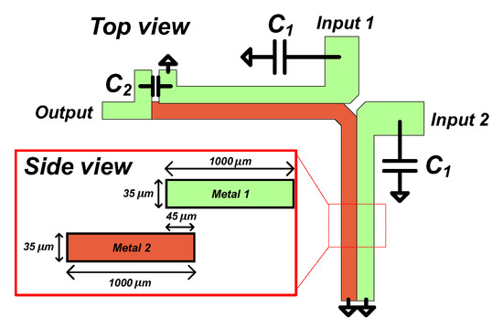
Figure 4.
Layout of the broadband lumped-distributed balun presented in [27].
Figure 5 shows photographs of the measurement setup and the fabricated lumped- distributed balun used as an outphasing combiner. A block diagram of the measurement setup is provided in Figure 6. To verify the operation of the outphasing combiner using a 10 MHz long-term evolution (LTE) signal at a carrier frequency of 650 MHz, the signal was decomposed into two outphased constant-envelope signals, and , using MATLAB. The decomposed signals were then downloaded into Rohde & Schwarz SMW 200A and SMM 100A vector signal generators, respectively. The output signals, reconstructed through the outphasing combiner, were measured using a Rohde & Schwarz FSW43 signal and spectrum analyzer. To validate the outphasing operation of the proposed balun combiner employing the 180° phase shift, the measured results were compared with those obtained using a broadband commercial Wilkinson combiner (model ZB2PD-63-2).
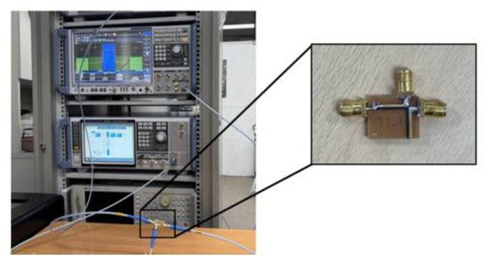
Figure 5.
Measurement setup with the fabricated lumped-distributed balun.
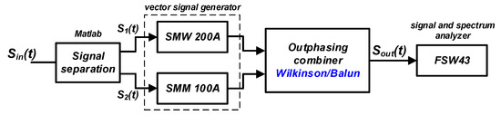
Figure 6.
Block diagram for the measurement setup of the outphasing combiner.
Figure 7 shows the measured adjacent channel leakage ratio (ACLR) for the output of the commercial Wilkinson combiner and the balun combiner, both with and without the 180° phase shift. The 180° phase shift was applied by directly adjusting the phase of the loaded signal in the vector signal generator. Without applying a DPD, the measured ACLR for the Wilkinson combiner is lower than −46 dBc. For the balun combiner, the measured ACLRs are lower than −13.5 dBc without the phase shift and lower than −46 dBc with the phase shift. These results demonstrate that the ACLR performance of the proposed balun combiner with the 180° phase shift is comparable to that of the commercial Wilkinson combiner. This confirms that the outphasing summation property can be achieved using the proposed balun combiner with the 180° phase shift, enabling accurate signal reconstruction.
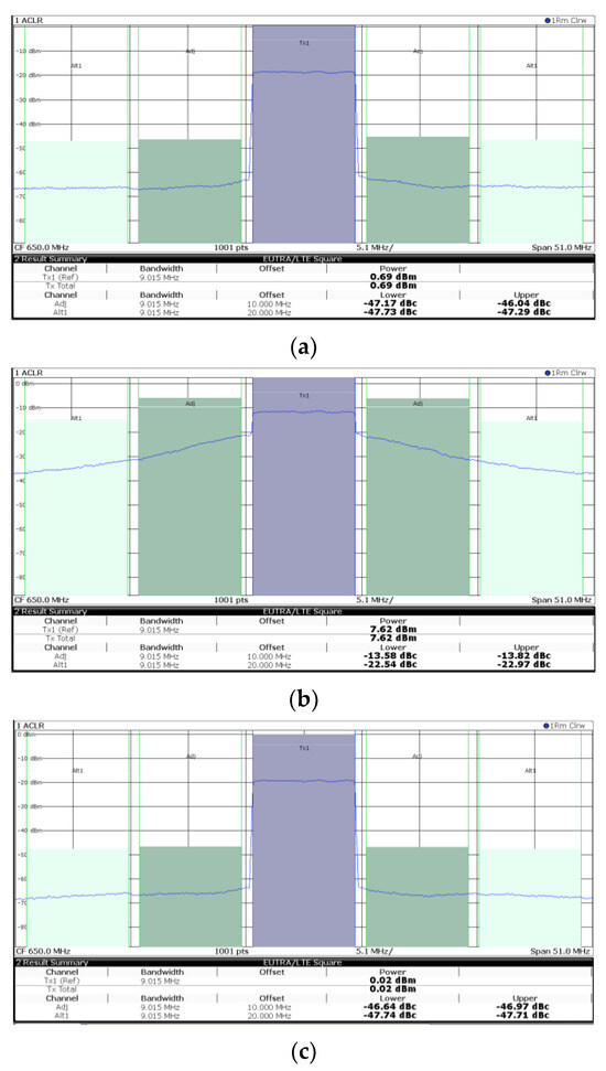
Figure 7.
Measured ACLR of (a) the Wilkinson combiner; (b) the balun combiner without the 180° phase shift; (c) the proposed balun combiner with the 180° phase shift.
Figure 8 compares the measured outphasing combining efficiency of the commercial Wilkinson combiner and the proposed balun combiner as a function of the outphasing angle at 650 MHz. The peak combining efficiency for the Wilkinson and proposed balun combiners is 96.3% and 92.6%, respectively. At 6 dB PBO, corresponding to = 60°, the Wilkinson combiner achieves approximately 24.8% efficiency, while the proposed balun combiner reaches 85.1%, representing a substantial improvement of nearly 60%. Figure 9 illustrates the combining efficiency of the proposed balun combiner across a wide frequency range from 360 to 860 MHz. Within this range, the measured peak combining efficiency spans from 86.3% to 93.3%, and the efficiency at 6 dB PBO ranges from 70.2% to 85.1%, demonstrating stable broadband performance.
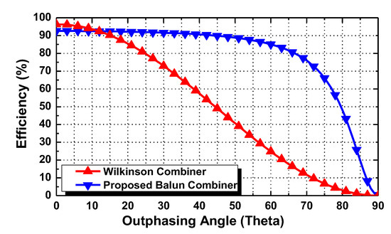
Figure 8.
Combining efficiency of the Wilkinson combiner and the proposed balun combiner versus outphasing angle.
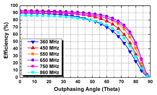
Figure 9.
Combining efficiency of the proposed balun combiner from 360 to 860 MHz.
4. Class-D Outphasing Power Amplifier with Proposed Balun Combiner
Figure 10 presents a simplified schematic of the proposed class-D PA with the proposed balun combiner, along with a driver stage and a series LC resonator. The class-D PA and its associated circuits including the driver chain are designed using an inverter-based topology in a 28 nm CMOS process. Each driver chain in the PA consists of two stages. The 180° phase shifter is realized using an additional inverter, as illustrated in Figure 10. The series LC resonator is highlighted in blue in Figure 10. A diode varactor (SMV1237) is integrated into the resonator to enable capacitance tuning, thereby supporting broadband operation. The inductor of the LC resonator is 5 nH, and the capacitance is tuned from 6.8 pF to 38.5 pF by varying the control voltage for the varactor diode. The bonding wire is connected to both the front and rear ends of the DA and PA, and a blocking capacitor is applied using off-chip components. The class-D PA was simulated using the measured S-parameter data of the proposed balun combiner. For performance comparison with the outphasing PA using the isolating combiner, a second simulation was conducted using the same PA structure with the S-parameter data of the commercial Wilkinson combiner. The supply voltages for the designed outphasing PA are 1.1 V for and 2.2 V for . The transistor widths of the NMOS and PMOS devices in each unit PA are 512 μm and 1024 μm, respectively.
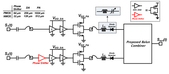
Figure 10.
Simplified schematic of proposed class-D PA with the proposed balun combiner.
Figure 11 shows the simulated voltage waveforms at the gate and drain of the class-D outphasing PA (i.e., the gate and drain of the power stage transistor) with the variation of . As illustrated in Figure 11a, the magnitudes of the gate voltage are sufficiently large for the device to perform a switching operation. Therefore, the magnitudes of the drain voltage are constant, behaving like an ideal voltage source, as shown in Figure 11b.
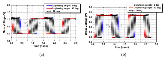
Figure 11.
Simulated waveforms of the class-D PA: (a) gate voltage; (b) drain voltage.
System-level simulation was conducted using co-simulation in Advanced Design System (ADS) and MATLAB to verify the outphasing operation. A block diagram of the system simulation setup is shown in Figure 12. The 10 MHz LTE signal was separated into two outphased signals in MATLAB and applied to the inputs of two class-D outphasing PAs. Figure 13 compares the simulated output spectrum of the class-D outphasing PA using three different combiners: the commercial Wilkinson combiner, the balun combiner without the 180° phase shift and the proposed balun combiner with the 180 phase shift. As shown in Figure 13, signal reconstruction was achieved for both the outphasing PA using the Wilkinson combiner and the outphasing PA using the proposed balun combiner with the 180° phase shift. At a 10 MHz offset from the 650 MHz carrier frequency, the Wilkinson combiner-based outphasing PA achieves an ACLR better than −45 dBc. In contrast, the balun-based outphasing PA without phase shift exhibits significant signal distortion, with an ACLR of −15 dBc. The proposed balun-based outphasing PA with the 180° phase shift achieves an ACLR of better than −40 dBc, indicating effective signal restoration. These results are consistent with the experimental measurements discussed in Section 3 and confirm that the outphasing PA with the proposed balun combiner successfully reconstructs the signal when the 180° phase shift is applied.
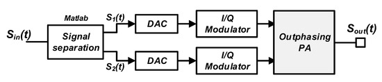
Figure 12.
Block diagram for simulation setup of the outphasing PA.
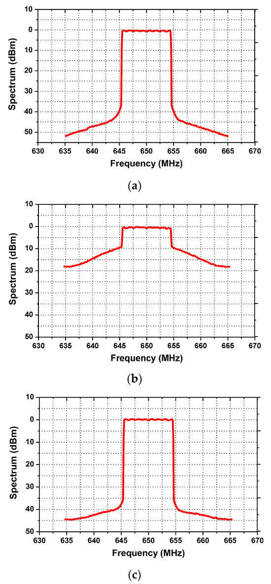
Figure 13.
Output spectrum of outphasing PA with (a) the Wilkinson combiner; (b) the balun combiner without 180 phase shift; (c) the proposed balun combiner with 180° phase shift.
Figure 14 and Figure 15 present the simulated drain efficiency (DE) and output power of the outphasing PA using the Wilkinson combiner and the proposed balun combiner as functions of the outphasing angle at 650 MHz. The DE is defined as the ratio of output power to the DC power consumption of the final class-D PA stage. The outphasing PA using the proposed balun combiner achieves a peak of 17.7 dBm with a corresponding peak DE of 82.9%. In comparison, the outphasing PA using the Wilkinson combiner reaches a peak of 17.7 dBm with a peak DE of 85.6%. At the 6 dB PBO ( = 60°), the outphasing PA using the proposed balun combiner achieves a DE of 61%, whereas the outphasing PA using the Wilkinson combiner achieves only about 24.1%, resulting in a DE difference of approximately 37%. Figure 16 shows the DEs of the outphasing PAs with the Wilkinson combiner and the proposed balun combiner as a function of output power. At peak power, the DEs of the outphasing PAs are similar for both combiners. But as the power is backed off, it can be observed that the proposed balun combiner exhibits better efficiency.
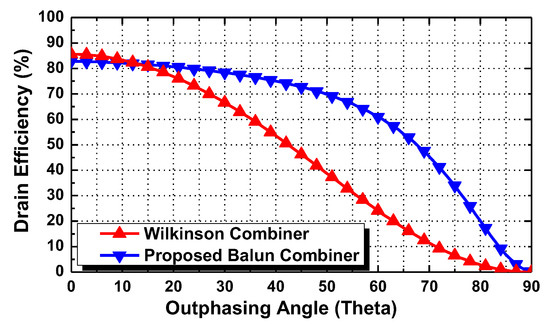
Figure 14.
DE of outphasing PA with the Wilkinson combiner and the proposed balun combiner versus outphasing angle.
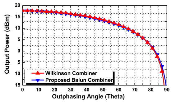
Figure 15.
Output power of outphasing PA with the Wilkinson combiner and the proposed balun combiner versus outphasing angle.
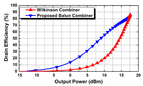
Figure 16.
DE versus output power of outphasing PA with the Wilkinson combiner and the proposed balun combiner.
Figure 17 illustrates the simulated DE of the outphasing PA using the proposed balun combiner across a frequency range from 360 to 860 MHz. The operating frequency was tuned by adjusting the capacitance of the LC filter through variation in the varactor voltage. Within this frequency range, the peak DE range from 77.2% to 82.9% and the simulated 6 dB PBO DE range from 53.9% to 61%, ensuring broadband operation.
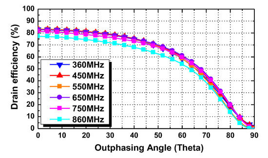
Figure 17.
DE of the outphasing PA with the proposed balun combiner from 360 to 860 MHz.
Table 1 compares the efficiency performance of outphasing PA using the Wilkinson combiner and the proposed balun combiner. While the peak efficiency of both outphasing PAs are comparable, the outphasing PA using the proposed balun combiner achieves approximately 36% higher efficiency at 6 dB PBO compared to the outphasing PA using the Wilkinson combiner. Furthermore, the ratio of the 6 dB PBO efficiency to peak efficiency for the outphasing PA using the proposed balun combiner is approximately 45% higher than that of the outphasing PA using the Wilkinson combiner. This result highlights the superior capability of the outphasing PA using the proposed balun combiner to maintain peak efficiency under PBO conditions, as compared to the outphasing PA with the isolating combiner. In addition, compared with other outphasing structures, the proposed structure can be designed with a relatively compact footprint while operating over a wide frequency range. Table 2 lists the performance of the proposed outphasing CMOS PA compared to other CMOS PAs. The table includes the performance of the state-of-the-art published CMOS PAs operating in the sub-GHz range. Compared with other outphasing CMOS PAs in [12,28,29], the proposed PA achieves the highest efficiency at 6 dB PBO. Thus, the proposed structure is a good candidate for 5G FR1 applications.

Table 1.
Performance comparison of outphasing combiner with class-D PA.
Table 2.
Performance comparison with CMOS PAs operating in the sub-GHz range.
5. Conclusions
This study analyzes both isolating and non-isolating outphasing combiners, including the commercial Wilkinson combiner and the proposed balun combiner employing the 180° phase shift. The two combiners were measured and compared in terms of ACLR and combining efficiency. A class-D outphasing PA was designed using measured S-parameter data for each combiner in a 28 nm CMOS process. For the proposed balun combiner alone, a measured ACLR of −46 dBc is achieved using a 10 MHz LTE signal without DPD, indicating effective signal reconstruction. At 6 dB PBO, the proposed balun combiner demonstrates a measured combining efficiency approximately 60% higher than that of the Wilkinson combiner. Similarly, system-level simulations confirm that the output spectrum of the class-D outphasing PA incorporating the proposed balun combiner matches the measured ACLR performance of the balun combiner alone, and reconstructs the original signal. In terms of DE, the outphasing PA with the proposed balun combiner achieves a simulated DE that is 37% higher than that of the outphasing PA using the Wilkinson combiner at 6 dB PBO. These results demonstrate that the proposed outphasing PA not only supports broadband operation and signal reconstruction but also achieves significantly higher efficiency under PBO conditions than the outphasing PA using the Wilkinson combiner, all within a compact implementation. Compared with other outphasing structures, the proposed structure can be designed with a relatively compact footprint while operating over a wide frequency range. In addition, the proposed architecture can be a good candidate for transceiver designs in 5G FR1 applications.
Author Contributions
Conceptualization and methodology, J.B. and O.L.; Investigation, J.B., M.J. and O.L.; formal analysis, J.B.; Circuit design and simulations, J.B.; Measurements, J.B. and M.J.; Comments and technical feedback, M.J., S.Y., I.N. and O.L.; Writing—original draft preparation, J.B.; Writing—review and editing, J.B., O.L., S.Y. and I.N.; supervision, O.L.; project administration, O.L. All authors have read and agreed to the published version of the manuscript.
Funding
This work was supported in part by the Institute of Information and communications Technology Planning and Evaluation (IITP), the Korea government (MSIT) (2022-0-00720, Development of W-band compact, high- efficiency, novel RF/power components for next-generation high-speed low-orbit satellite communications), and in part by the National Research Foundation of Korea (NRF) grant funded by the Korea government (MSIT) (No. RS-2023-00277075). The CAD tools were supported by IDEC.
Data Availability Statement
Data are contained within the article.
Conflicts of Interest
The authors declare no conflicts of interest.
References
- Cox, D. Linear amplification with nonlinear components. IEEE Trans. Commun. 1974, 22, 1942–1945. [Google Scholar] [CrossRef]
- Chireix, H. High-Power Outphasing Modulation. Proc. Inst. Radio Eng. 1935, 21, 1370–1392. [Google Scholar] [CrossRef]
- Xu, H.; Palaskas, Y.; Ravi, A.; Sajadieh, M.; El-Tanani, M.A.; Soumyanath, K. A flip-chip-packaged 25.3 dBm class-D outphasing power amplifier in 32 nm CMOS for WLAN application. IEEE J. Solid-State Circuits 2011, 46, 1596–1605. [Google Scholar] [CrossRef]
- Pham, A.; Sodini, C.G. A 5.8 GHz, 47% efficiency, linear outphase power amplifier with fully integrated power combiner. In Proceedings of the IEEE Radio Frequency Integrated Circuits (RFIC) Symposium, San Francisco, CA, USA, 10–13 June 2006; pp. 157–160. [Google Scholar]
- Hakala, I.; Choi, D.K.; Gharavi, L.; Kajakine, N.; Koskela, J.; Kaunisto, R. A 2.14-GHz Chireix outphasing transmitter. IEEE Trans. Microw. Theory Tech. 2005, 53, 2129–2138. [Google Scholar] [CrossRef]
- Raab, F. Efficiency of outphasing RF power-amplifier systems. IEEE Trans. Commun. 1985, 33, 1094–1099. [Google Scholar] [CrossRef]
- Hakala, I.; Gharavi, L.; Kaunisto, R. Chireix power combining with saturated class-B power amplifiers. In Proceedings of the 34th European Microwave Conference, Amsterdam, The Netherlands, 12–14 October 2004; pp. 1–4. [Google Scholar]
- Qureshi, J.H.; Pelk, M.J.; Marchetti, M.; Neo, W.E.; Gajadharsing, J.R.; van der Heijden, M.P.; De Vreede, L.C.N. A 90-W peak power GaN outphasing amplifier with optimum input signal conditioning. IEEE Trans. Microw. Theory Tech. 2009, 57, 1925–1935. [Google Scholar] [CrossRef]
- Aggrawal, E.; Rawat, K. Reconfigurable Chireix outphasing power amplifier over multiple frequency bands. IEEE Trans. Circuits Syst. II Express Briefs 2019, 67, 1019–1023. [Google Scholar] [CrossRef]
- Calvillo-Cortes, D.A.; van der Heijden, M.P.; Acar, M.; de Langen, M.; Wesson, R.; van Rijs, F.; de Vreede, L.C. A package-integrated Chireix outphasing RF switch-mode high-power amplifier. IEEE Trans. Microw. Theory Tech. 2013, 61, 3721–3732. [Google Scholar] [CrossRef]
- Calvillo-Cortes, D.A.; van der Heijden, M.P.; de Vreede, L.C. A 70W package-integrated class-E Chireix outphasing RF power amplifier. In Proceedings of the 2013 IEEE MTT-S International Microwave Symposium Digest (MTT), Seattle, WA, USA, 2–7 June 2013; pp. 1–3. [Google Scholar]
- Hur, J.; Kim, H.; Lee, O.; Kim, K.W.; Bien, F.; Lim, K.; Lee, C.H.; Laskar, J. A multilevel class-D CMOS power amplifier for an out-phasing transmitter with a nonisolated power combiner. IEEE Trans. Circuits Syst. II Express Briefs 2016, 63, 618–622. [Google Scholar] [CrossRef]
- Xu, H.; Palaskas, Y.; Ravi, A.; Sajadieh, M.; Elmala, M.; Soumyanath, K. A 28.1 dBm class-D outphasing power amplifier in 45 nm LP digital CMOS. In Proceedings of the 2009 Symposium on VLSI Circuits, Kyoto, Japan, 16–18 June 2009; pp. 206–207. [Google Scholar]
- Tai, W.; Xu, H.; Ravi, A.; Lakdawala, H.; Bochobza-Degani, O.; Carley, L.R.; Palaskas, Y. A transformer-combined 31.5 dBm outphasing power amplifier in 45 nm LP CMOS with dynamic power control for back-off power efficiency enhancement. IEEE J. Solid-State Circuits 2012, 47, 1646–1658. [Google Scholar] [CrossRef]
- Fritzin, J.; Svensson, C.; Alvandpour, A. A 32 dBm 1.85 GHz class-D outphasing RF PA in 130 nm CMOS for WCDMA/LTE. In Proceedings of the 2011 IEEE European Solid State Circuits Conference (ESSCIRC), Helsinki, Finland, 12–16 September 2011; pp. 127–130. [Google Scholar]
- Li, S.; Huang, M.Y.; Jung, D.; Huang, T.Y.; Wang, H. A MM-wave current-mode inverse outphasing transmitter front-end: A circuit duality of conventional voltage-mode outphasing. IEEE J. Solid-State Circuits 2020, 56, 1732–1744. [Google Scholar] [CrossRef]
- Zhang, X.; Larsen, L.E.; Asbeck, P.M. Design of Linear RF Outphasing Power Amplifier; Artech House: Boston, MA, USA, 2003. [Google Scholar]
- Shi, B.; Sundstrom, L. Investigation of a highly efficient LINC amplifier topology. In Proceedings of the Vehicular Technology Conference, Atlantic City, NJ, USA, 7–11 October 2001; pp. 1215–1219. [Google Scholar]
- Yao, Y.; Long, S. Power amplifier selection for LINC applications. IEEE Trans. Circuits Syst. II Express Briefs 2008, 53, 763–767. [Google Scholar] [CrossRef]
- Pozar, D.-M. Microwave Engineering, 4th ed.; Wiley: New York, NY, USA, 2011. [Google Scholar]
- Marchand, N. Transmission line conversion transformers. Electron 1944, 17, 142–145. [Google Scholar]
- Liu, J.X.; Hsu, C.Y.; Chuang, H.R.; Chen, C.Y. A 60-GHz millimeter-wave CMOS Marchand balun. In Proceedings of the 2007 IEEE Radio Frequency Integrated Circuits (RFIC) Symposium, Honolulu, HI, USA, 3–5 June 2007; pp. 445–448. [Google Scholar]
- Ojha, S.P.; Branner, G.R.; Kumar, B.P. A miniaturized lumped-distributed balun for modern wireless communication systems. In Proceedings of the 39th Midwest Symposium on Circuits and Systems, Ames, IA, USA, 21 August 1996; pp. 1347–1350. [Google Scholar]
- Tang, C.W.; Chang, C.Y. A semi-lumped balun fabricated by low temperature co-fired ceramic. In Proceedings of the 2002 IEEE MTT-S International Microwave Symposium Digest, Seattle, WA, USA, 2–7 June 2002; pp. 2201–2204. [Google Scholar]
- Ang, K.S.; Leong, Y.C.; Lee, C.H. Analysis and design of miniaturized lumped-distributed impedance-transforming baluns. IEEE Trans. Microw. Theory Tech. 2003, 51, 1009–1017. [Google Scholar]
- Wang, F.; Wang, H. A broadband linear ultra-compact mm-wave power amplifier with distributed-balun output network: Analysis and design. IEEE J. Solid-State Circuits 2021, 56, 2308–2323. [Google Scholar] [CrossRef]
- Oh, K.; Yoo, S.; Lee, O. Design of a Compact-Sized Broadband Lumped-Distributed Balun Including Impedance Matching. J. Korean Inst. Electromagn. Eng. Sci. 2022, 33, 911–918. [Google Scholar] [CrossRef]
- Rawat, A.S.; Rajendran, J.; Mariappan, S.; Kumar, N.; Mak, P.I.; Martins, R.P. A 27-dBm, 0.92-GHz CMOS Power Amplifier with Mode Switching and a High-Q Compact Inductor (HQCI) Achieving a 30% Back-Off PAE. IEEE Trans. Circuits Syst. II Express Briefs 2022, 70, 121–125. [Google Scholar] [CrossRef]
- Ginzberg, N.; Cohen, E. A wideband CMOS power amplifier with 52% peak PAE employing resistive shunt feedback for sub-6 GHz 5G applications. IEEE Microw. Wirel. Compon. Lett. 2022, 33, 192–195. [Google Scholar] [CrossRef]
- Ding, L.; Hur, J.; Banerjee, A.; Hezar, R.; Haroun, B. A 25 dBm outphasing power amplifier with cross-bridge combiners. IEEE J. Solid State Circuits 2015, 50, 1107–1116. [Google Scholar] [CrossRef]
- Hung, T.P.; Choi, D.K.; Larson, L.E.; Asbeck, P.M. CMOS outphasing class-D amplifier with Chireix combiner. IEEE Microw. Wirel. Compon. Lett. 2007, 17, 619–621. [Google Scholar] [CrossRef]
Disclaimer/Publisher’s Note: The statements, opinions and data contained in all publications are solely those of the individual author(s) and contributor(s) and not of MDPI and/or the editor(s). MDPI and/or the editor(s) disclaim responsibility for any injury to people or property resulting from any ideas, methods, instructions or products referred to in the content. |
© 2025 by the authors. Licensee MDPI, Basel, Switzerland. This article is an open access article distributed under the terms and conditions of the Creative Commons Attribution (CC BY) license (https://creativecommons.org/licenses/by/4.0/).