Abstract
A zero-voltage switching (ZVS) push–pull self-oscillating arc ignition circuit was proposed, marking the first application of ZVS technology in welding arc ignition systems. The circuit’s working principle was analyzed, and time-domain waveforms of the switching transistors verified the realization of soft switching. A conducted interference test platform was established in order to assess the circuit’s electromagnetic compatibility under no-load and arc ignition transient conditions. In comparison with conventional domestic arc ignition circuits, the proposed ZVS circuit demonstrated substantially diminished quasi-peak interference levels, with a reduction exceeding 9.5 dB in both instances. Additionally, under no-load conditions, the ZVS circuit demonstrated interference levels comparable to those of a commercial Fronius system, while during arc ignition transients, it exhibited an over 5 dB reduction. The findings of this study demonstrate that the incorporation of soft-switching techniques into arc ignition circuits can effectively mitigate conducted interference, thus providing a promising and practical approach for industrial welding equipment.
1. Introduction
The year 2020 marked the release of the electromagnetic compatibility standard GB/T 15579.10 [1] for arc welding equipment in China, which represented a further increase in the requirements for electromagnetic interference of arc welding power sources. TIG (Tungsten Inert Gas) welding, a high-precision welding process, has found extensive application in the aerospace and nuclear industries due to its ability to produce excellent welding quality [2,3]. However, due to the existence of high-frequency and high-voltage arc ignition, the interference hazard is the greatest in the arc welding power source category. This has the potential to affect not only peripheral equipment, such as communication interruptions, data loss and precision instrumentation measurement errors, but also to cause serious safety hazards [4]. The existing research in this field has focused primarily on the development of arc ignition methods [5,6,7]. For instance, Pang [8] utilized high voltage arc ignition for micro-TIG welding, enhancing the stability of arc initiation through the optimization of the arc oscillation triggered by cathode spot (CSM) motion. Liu [9] proposed an arc ignition technique based on arc thermal conversion and elucidated its mechanism. This technique used the Joule heat generated by contact to form a metal bridge, which was evaporated by the electrode rotation and mechanical force to generate an arc. Tang [10] investigated the arc ignition process in TIG-MIG composite welding and examined the impact of altering parameters such as the welding torch tilt angle on the regularity of auxiliary arc ignition. Xia [11] investigated the TIG arc ignition method based on a 1000 W semiconductor laser. The research on electromagnetic interference of arc welding power supply mainly focuses on the simulation analysis of interference and filter design [12,13,14,15,16], and there is almost no research on the interference of arc ignition. Interference is primarily propagated by radiation and conduction in two ways. Conduction interference is directly coupled to sensitive equipment through power lines and other conductors. This form of interference is often more direct and difficult to inhibit. This is the focus of the optimization of electromagnetic compatibility design. In this paper, a novel arc ignition circuit for TIG welding machines is proposed, and the conducted interference is quantitatively analyzed with the objective of reducing the interference during the arc ignition process of TIG welding. This is of significant value for engineering applications. Moreover, future manufacturing systems may rely on satellite links for global connectivity [17]. In such environments, high-frequency interference from welding—especially during arc ignition—can compromise data integrity and communication reliability. Reducing EMI in the ignition stage is thus essential for ensuring stable operation in communication-sensitive applications.
2. Hardware Test Platforms
The conducted interference test platform has been constructed in accordance with the provisions stipulated in the standard GB 4824 [18]. This standard is instrumental in regulating the RF Emission characteristics, limits and measurement methodologies for industrial, scientific and medical equipment. It is notable that the standard does not provide a clear limit for the conducted interference in the arc ignition process.
The conducted interference test platform consists of a welding system, a linear impedance stabilization network (LISN), an isolation transformer, a spectrum analyzer, a digital oscilloscope, and a high-voltage probe, as demonstrated in Figure 1.
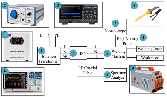
Figure 1.
Structure of conducted interference testing platform.
The welding machine is a single-phase TIG welding power supply model WS-250S manufactured in China. The linear impedance stabilizing network is the EM5040B from Zhiyong Company (Shenzhen, China), and the high pass filter at the output is set to 150 KHz. The oscilloscope employed is the SDS824X four-channel oscilloscope from Tingyang Company (Shenzhen, China). The interference receiver is a Goodwell GSP-818 spectrum analyzer, which has an EMI mode and complies with the international electromagnetic compatibility standard CISPR 16-1-1 [19]. The resolution bandwidth (RBW) and the video bandwidth (VBW) are set to 9 kHz according to the standard. The starting frequency is set to 150 kHz, and the ending frequency is set to 30 MHz.
3. Hardware Circuit Comparison and Design
3.1. Original Arc Ignition Circuit Design
The arc ignition circuit, a component of welding machines, is a subject of current interest in the domestic market. Despite the numerous variations, the fundamental differences among them are not significant. The original arc ignition circuit illustrated in Figure 2 will be employed for the purpose of comparison and analysis. It is composed of three primary circuits: the step-up main circuit, the step-up control circuit, and the oscillation coupling circuit. The step-up main circuit consists of the secondary center tap coil L1 of the inverter transformer, diodes D1-D4, DC boost high voltage pack T1, and R1C1 filter circuit. The step-up control circuit consists of an eight-legged relay K1, a switching tube Q1, and other associated components. The oscillating coupling circuit consists of a spark gap HF, a high-voltage capacitor C5 and a coupling inductor T2. The secondary side of the coupled inductor is connected to the main circuit of the welder via the secondary boost.
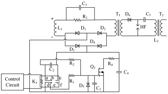
Figure 2.
The original arc ignition circuit.
The operation of the circuit is facilitated by the switching of Q1, resulting in an alternating current (AC) square wave voltage being generated on L1. When the voltage is positive half-wave, D1 and D4 are conducting, and negative half-wave voltage is present in D2 and D3. When the arc ignition circuit functions, the control signal input to the eight-pin relay K1 results in the closure of normally closed contacts ab, de and the opening of normally open contacts ac, df. The positive half-wave through the filter circuit R1C1 results in the flow of current through the diode D4 (contact c, contact a). The gate starter resistor R2 activates the switch Q1, enabling the current to flow through D4, R4 into Q1, and finally from the diode D1 back to the L1. The negative half of the work process is analogous. Following the T1 DC high-voltage packet boost, the oscillator capacitor C5 is charged, and the breakdown spark gap HF is established, in a manner analogous to the RLC attenuation oscillation.
3.2. Zero-Voltage Switching Arc Ignition Circuit Operation Principle
As illustrated in Figure 3, the proposed zero-voltage switching arc ignition circuit has been designed. The output of the inverter circuit, which is part of the transformer side square wave voltage, is rectified by the DC-DC module. The design utilizes the VRB4812LD-50W module manufactured by Jin Sheng Yang (MORNSUN). The input voltage of this module ranges from 60 V to 12 V DC, with an output current of up to 4167 mA and a maximum output power of 50 W. The power module’s primary parameters and indicators are delineated in Table 1. The output of this is 12 V, which is connected to the VCC. The subsequent progression involves the utilization of a zero-voltage push–pull self-excited circuit, which is integrated with the DC high-voltage package T1 to facilitate a boost. Following this boost, the capacitor C3 undergoes a charging phase, subsequently leading to a breakdown spark gap HF, akin to the RLC attenuation oscillator. Finally, the coupled inductor T2 provides a secondary boost to the main circuit of the welder.
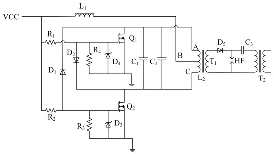
Figure 3.
ZVS zero voltage switching arc ignition circuit.

Table 1.
Parametric indicators of the DC-DC module.
The operation of the circuit is outlined as follows [20,21], where iL1 denotes the current in the choke inductor, and the potentials at A and C represent the potentials of the drains of MOS tubes Q1 and Q2, which are denoted by uA and uC, respectively. The current flowing into the drain D of Q1 and Q2 is represented by iQ1 and iQ2, respectively. The potential of the center tap B is represented by uB. The voltages at the extremities of capacitors C1 and C2 are designated as u1.
The start-up phase is as follows: When the ZVS circuit is powered up, the current in the choke inductor L1 is zero, and then the inductor current starts to increase. Concurrently, the current reaches the gate of the MOS tube via the gate startup resistors R1 and R2 and the voltage regulator diodes D3 and D4 after clamping. It is important to note that due to the difference in semiconductor devices, iQ1 and iQ2 are not equal. Assuming that iQ1 > iQ2, the excitation current on L2 generates a positive induced voltage and a negative induced voltage. L2 and C1, C2 resonance occurs in parallel. At this time, where uA ≈ 0, the gate voltage of Q2 is pulled down and cutoff.
The first operating state is defined as follows: Q1 conduction, the previous state iL2 direction from A to C, and the resonant capacitor voltage is zero. Given the impossibility of sudden alteration to the inductor current, the inductor charges the capacitors, resulting in a polarity of C positive and A negative. Consequently, the voltage at point A is pulled down to 0 V, thereby establishing a sinusoidal voltage at point C and inducing a sinusoidal state in iL2. It is notable that when iL2 = 0, the voltage of C1 and C2 reaches its maximum value. Q1 is characterized by a constant state of activation.
Operating state 2 is characterized by the discharge of C1 and C2 from L2, with iL2 undergoing a sinusoidal increase from C to A. It is noteworthy that this sinusoidal increase in iL2 is concurrent with the discharge of the resonant capacitor. The inductor current iL2 reaches its maximum value when the resonant capacitor is discharged.
Operating state 3: L2 is responsible for charging the resonant capacitor, and the voltage polarity is A positive, C negative. The gate voltage of Q2 increases, and finally Q2 conducts and Q1 cuts off. In the context of a stable supply voltage, the alternation of conduction in Q1 and Q2 gives rise to a self-excited LC oscillation.
The maximum value of voltage u1 across the capacitor is constrained by the following equation:
u1 = VCC × π
The above equation demonstrates that the withstanding voltage of the resonant capacitor, in conjunction with that of the mosfet, is contingent on the supply voltage. In the context of mosfet selection, it is imperative to exercise caution with regard to the device parameters, as this particular topology necessitates a pronounced emphasis on the mosfet voltage withstand. The selection of the resonant switch is made with Infineon’s IRFP260NPBF mosfet. The device has been engineered to possess a 200 V drain source breakdown voltage and 50 A continuous drain current capability. This ensures that it meets the requirements of low-voltage high-current arc-inducing circuits on the voltage margin and current carrying capacity. The output capacitance Coss of 603 pF has been demonstrated to reduce turn-off losses in the ZVS mode and to control the resonant frequency within a reasonable range. In addition, the on-resistance of 40 mΩ has been shown to help suppress on-resistance losses.
The resonant frequency, f, of LC parallel resonance is expressed by the following equation:
The peak current im2 on the resonant inductor L2 is constrained by the following equation:
It can thus be concluded that the oscillation frequency of the circuit is set to approximately 15 kHz. The resonant capacitors C1 and C2 are 100 nF, and the resonant inductance is 560 µH.
3.3. Parametric Design of Oscillatory Coupling Circuits
The equivalent circuit of the RLC oscillation circuit is illustrated in Figure 4, which corresponds to the spark gap HF, the resonant capacitance C3 and the primary inductance of the coupling coil T2 in Figure 3. R represents the equivalent resistance of the circuit, including the resistance of the spark gap at the moment of discharge and the line resistance of the attenuating oscillation.
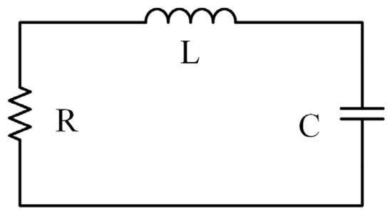
Figure 4.
Equivalent loop of an oscillating coupled circuit.
In the context of a series RLC circuit, the current i is expressed by Kirchhoff’s voltage law as follows:
As demonstrated in the aforementioned differential equation, the circuit underdamped response must satisfy the condition that the damping coefficient, denoted by ξ, is less than one. The expression for the damping coefficient is as follows:
It is evident that the line resistance in the actual circuit and the total resistance during spark discharge are not negligible [22]. The damped oscillation frequency, fd, satisfies the following expression:
The process resistance of the spark gap and the line resistance are not easily measurable parameters. Thus, Formulas (5) and (6) can be derived from the under-damped oscillation frequency, fd, coupling inductance, L, and oscillation capacitance, C, in the under-damped oscillation conditions of the relationship expressed by Formula (7).
In the preceding analysis, the oscillation frequency is derived based on ideal lumped components. It is acknowledged that distributed parasitic capacitances and inductances have the capacity to introduce slight shifts to the practical resonant frequency. However, it is anticipated that their magnitude will be relatively negligible in this design.
According to the damped oscillation frequency, an increase in capacitance C will lead to a decrease in fd. Concurrently, an increase in capacitance will enhance energy storage capacity, thereby amplifying the discharge strength and resulting in an under-damped oscillation. This, in turn, will increase the amplitude and duration of the input side of the conduction interference, and concurrently, it may cause the circuit to transition out of the under-damped response state. Conversely, a decrease in capacitance C will stabilize the under-damped oscillation, and concurrently, as fd rises, the energy will be distributed to multiple oscillation voltages, thereby reducing the single peak voltage and assisting in the reduction of interference at the input side. However, it is imperative to ensure that the cold welding arc requirements are met. It is evident that decreasing capacitance C will stabilize the underdamped oscillation, while an increase in fd will result in the energy being allocated to multiple oscillation voltages, thereby reducing the single peak voltage. This, in turn, is beneficial in reducing interference at the input side. However, it is imperative to ensure that the arc requirements of the cold welding are met. The analysis of the oscillation parameters reveals that the oscillation coupling capacitor should be constructed using 470 pF, 5 kV high-voltage ceramic capacitors, and inductors employing a ferrite core, with eight turns of wire measuring 5.14 µH.
The proposed ZVS arc ignition circuit demonstrates good potential for industrial implementation. Its simple topology allows for seamless integration with existing welding power supplies. By utilizing readily available components and avoiding complex control systems, the circuit remains cost-effective. Additionally, the design is compatible with standard PCB manufacturing and assembly processes, supporting scalability and mass production.
4. Circuit Verification and Test Results
4.1. Circuit Verification
Following a thorough analysis of the principle and the design of the hardware, the waveforms of the soft-switching arc ignition circuit are verified on the WS-250S welding machine.
4.1.1. Zero-Voltage Switching Circuit Waveforms
As demonstrated in Figure 5, the gate voltage of the MOS tube exhibits fluctuations, indicating that the circuit is operating in self-excited oscillation mode. The two switching tubes are alternately turned on and off, forming a symmetrical operating state.
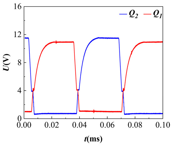
Figure 5.
Gate voltage waveform of a switching tube.
The signal condition of the MOS tube is illustrated in Figure 6. The electrical signals under single turn-on and turn-off conditions demonstrate that the ZVS zero-voltage switching circuit exhibits a negligible turn-on loss during the turn-on and turn-off process of the switch. Furthermore, the switch has achieved a quasi-resonant state in the self-excited state. However, it should be noted that the switching loss remains unavoidable due to the limited resonant energy.
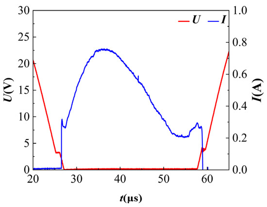
Figure 6.
Electrical signals at the ends of the switching tubes.
As demonstrated in Figure 7, the output voltage waveform on the primary inductor L2 of the DC high-voltage packet is shown, and the LC resonant frequency is 15.4 kHz. The resonant sinusoidal peak voltage is approximately 38 V, and the resonant frequency and the sinusoidal peak voltage are consistent with the result of Equation (2).
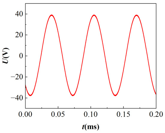
Figure 7.
LC resonant output voltage waveform.
4.1.2. Oscillating Coupled Circuit Waveforms
As illustrated in Figure 8, the output voltage of the coupling inductor T2 on the secondary side of the oscillatory coupling circuit is depicted under undamped response. The underdamped oscillation frequency fd is approximately 2.17 MHz, and the peak voltage of the underdamped oscillation is 2400 V. It has been verified that the oscillation parameters and frequency conditions described above satisfy the conditions of the underdamped response in Equation (7).
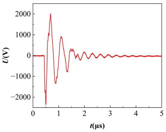
Figure 8.
Voltage waveforms on the secondary side of an oscillator-coupled circuit.
4.2. Conducted Interference Test
The present study is based on the conducted interference test platform on the welding power supply under different conditions of the arc ignition circuit on the input side of the live wire and the neutral wire of the conducted interference test. The test is comprised of two distinct states: the no-load interference test, defined as the state in which the arc has not been initiated, although the arc ignition circuit functions within normal parameters. The second state is the arc ignition instantaneous interference test, which involves the use of a fixed torch to position the tungsten electrode at a distance of 1 mm from the workpiece during a standard welding arc test.
The detection mode is in accordance with the requirements of the GB/T 15579.10 standard, employing quasi-peak detection as outlined in [23,24]. The findings of the study indicate that the data obtained from the live wire and the neutral wire are almost identical. Consequently, the quasi-peak value of the live wire is selected as a representative interference characteristic parameter for analysis.
4.2.1. Interference Test with No Load on the Soldering Gun
In the experimental setup, the WS-250S welding power supply was employed in conjunction with the original arc ignition circuit in the argon arc welding mode for the torch no-load interference test. To facilitate a comparative analysis, the ZVS arc ignition circuit was utilized for a comparative test. The quasi-peak test results on the live wire of the spectrum analyzer are shown in Figure 9.
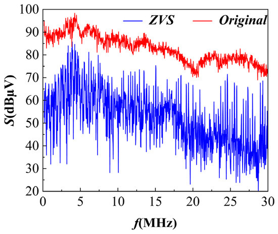
Figure 9.
The quasi-peak detection spectrum of the live wire.
The experimental findings demonstrate that the maximum amplitude of the quasi-peak detected wave on the live wire of the original arc ignition circuit is 98.37 dBµV. Following the implementation of the ZVS arc ignition circuit for the conducted interference test, it was determined that the maximum amplitude of the quasi-peak detected wave on the live wire was reduced to 85.76 dBµV. The maximum decibel difference of the quasi-peak detected wave on the live wire is 12.61 dB, which is equivalent to the voltage amplitude reduced to about 23.4% of the original amplitude. This reduction corresponds to a reduction in the voltage amplitude to about 23.4% of the original amplitude. This finding indicates that the ZVS circuit is capable of effectively mitigating the conducted interference caused by the arcing voltage on the input side of the torch when the torch is unloaded.
4.2.2. Arc Ignition Instantaneous Interference Test
The instant of arc initiation is a very brief process, necessitating the setting of the maximum hold function of the spectrum analyzer for the purposes of testing. The distance between the tungsten electrode and the workpiece is 1 mm. The test involves a comparison between the original arc ignition circuit and the ZVS arc ignition circuit. The results of the quasi-peak detection on the live wire are shown in Figure 10. The maximum interference value of quasi-peak detection on the live wire is 79.78 dBµV for the original arc ignition circuit. Subsequent to conducting interference tests on the ZVS arc ignition circuit, it was ascertained that the maximum interference value of quasi-peak detection on the live wire had been reduced to 70.26 dBµV. The maximum decibel difference of quasi-peak interference on the live wire is 9.52 dB, which reduces the corresponding voltage amplitude to 33.4% of the original amplitude. Consequently, the ZVS circuit demonstrates superiority over the original circuit with respect to input interference at the moment of arc ignition.
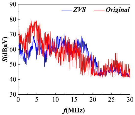
Figure 10.
The quasi-peak interference spectrum of the live wire at the moment of arc ignition.
4.3. Product Comparison Analysis
In order to verify the design reliability of the arc ignition circuit, a comparison is made between the WS-250S welding power supply equipped with ZVS arc ignition circuit and the iWave 230i from Fronius. The quasi-peak frequency spectrum of the live wire for the instantaneous interference between the no-load and arc ignition moment of the welding torch is shown in Figure 11.
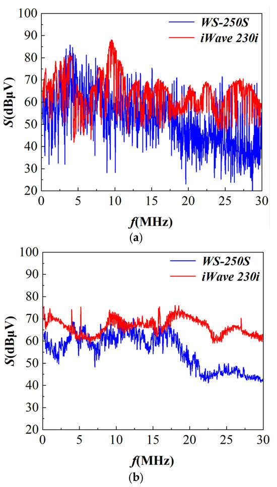
Figure 11.
The quasi-peak interference spectrum of the live wire of iWave 230i and WS-250S: (a) the moment when the arc voltage is unloaded; (b) at the moment of arc ignition.
As shown in Figure 11a, in the no-load interference test of the welding torch, the maximum interference value of the quasi-peak detection mode on the live wire is 88.1 dBµV. A comparison and analysis with the welding power supply equipped with the ZVS arc ignition circuit reveals that the interference level of the ZVS arc ignition circuit is lower than that of mainstream products in the no-load interference test, and the overall performance is comparable to that of the existing products, with the amplitude of the interference voltage in a similar range.
As shown in Figure 11b, the arc instantaneous interference test on the live wire quasi-peak detector interference maximum value was found to be 76.03 dBµV. A comparison of the ZVS arc ignition circuit with mainstream products in the input side of the interference spectrum found in the arc instantaneous test on the live wire quasi-peak detector reveals that the ZVS arc ignition circuit has an interference maximum value of the quasi-peak detector spectrum that is approximately 5.77 dB lower than that of mainstream products. Furthermore, the voltage amplitude is reduced to 51.5%, verifying that the design of ZVS is able to suppress high-frequency interference. It is noteworthy that Fronius incorporates a dedicated EMI filter on the input side, while domestic welders generally lack such a feature, thereby further substantiating the superiority of the arc ignition circuit.
5. Conclusions
This study innovatively integrates zero-voltage switching (ZVS) technology with oscillatory coupling principles to design a new type of arc ignition circuit, addressing the persistent issue of electromagnetic interference during arc initiation. This paper is the first to document the implementation of ZVS in welding arc ignition systems. A conducted interference test platform was established in accordance with the provisions of the GB 4824 standard, encompassing both torch no-load and arc transient conditions. A quantitative analysis was conducted in accordance with the provisions of GB/T 15579.10, with the objective of evaluating the input-side interference.
The experimental findings indicate that, under conditions of no load, the maximum voltage amplitude was diminished to 23.4% of its original value. This is equivalent to a 12.61 dB reduction in interference. During the occurrence of arc transients, the amplitude underwent a decrease to 33.4%, accompanied by a 9.52 dB reduction. The findings of this study suggest that the proposed circuit is capable of achieving a conducted interference level that is comparable to that of mainstream commercial systems. This outcome serves as a testament to the practical viability of the circuit. Moreover, the successful implementation of soft switching in arc ignition circuits introduces a new approach to improving electromagnetic compatibility in welding technology.
Author Contributions
Conceptualization, X.L.; Methodology, Y.L.; Software, Y.L.; Validation, Y.L.; Data curation, Y.L.; Writing—original draft preparation, Y.L.; Writing—review and editing, X.L.; Visualization, Y.L.; Supervision, X.L.; Project administration, X.L.; Funding acquisition, X.L. All authors have read and agreed to the published version of the manuscript.
Funding
This work was supported by the National Natural Science Foundation of China (Grant No. 52075372).
Data Availability Statement
Data are contained within the article.
Conflicts of Interest
The authors declare no conflicts of interest.
References
- GB/T 15579.10; Arc Welding Equipment—Part 10: Electromagnetic Compatibility (EMC) Requirements. National Technical Committee for Standardization of Electric Welding Machines: Beijing, China, 2020.
- Sonar, T.; Balasubramanian, V.; Malarvizhi, S.; Venkateswaran, T.; Sivakumar, D. Maximizing strength and corrosion resistance of InterPulsed TIG welded Superalloy 718 joints by RSM for aerospace applications. CIRP J. Manuf. Sci. Technol. 2021, 35, 474–493. [Google Scholar] [CrossRef]
- Gao, Y.; Ren, B.; Chen, Y.; Sui, X.; Zhao, X.; Fan, C.; Chen, C. Improvement of Formation, Microstructure and Mechanical Properties of TIG Welded TC4 Titanium Alloy by Ultrasonic Coaxial Radiation. Acta Metall. Sin. 2024, 37, 2045–2056. [Google Scholar] [CrossRef]
- Nice, D.M.; Kiger, C.J. Electromagnetic compatibility concerns of in-situ welding on instrumentation and control systems. In Proceedings of the 9th International Topical Meeting on Nuclear Plant Instrumentation, Control, and Human-Machine Interface Technologies, Charlotte, NC, USA, 22–26 February 2015. [Google Scholar]
- Zang, Y.; Jia, M.; Zhang, Z.; Cui, W. Experimental Investigation on Gliding Arc Plasma Ignition and Assisted Combustion Actuator. IEEE Trans. Plasma Sci. 2023, 51, 127–139. [Google Scholar] [CrossRef]
- Park, M.; Hirata, Y.; Urabe, T. Development of controlled micro-discharge at the atmospheric pressure. Weld. World 2014, 58, 47–54. [Google Scholar] [CrossRef]
- Tsukamoto, M.; Murai, K.; Tanaka, M.; Kayahara, T.; Abe, N.; Nakata, K.; Ushio, M. Pulsed laser focusing for triggering discharge in arc welding system. Q. J. Jpn. Weld. Soc. 2005, 23, 265–269. [Google Scholar] [CrossRef]
- Pang, S.; Cao, B. Low current arc ignition stability in micro-TIG welding. J. Manuf. Process. 2021, 69, 12–20. [Google Scholar] [CrossRef]
- Liu, K.; Khan, M.A.; Zhou, Z.; Song, D.; Zhou, J. High-efficiency DC-SEAM for aerospace materials with Joule-arc heat transition and ignition mechanism. CIRP J. Manuf. Sci. Technol. 2023, 41, 216–224. [Google Scholar] [CrossRef]
- Tang, Y.; Zhu, Z.; Yang, Z.; Fu, P.; Yu, Y. TIG arc-induced non-contact MIG arc ignition. J. Mater. Process. Technol. 2018, 257, 45–53. [Google Scholar] [CrossRef]
- Xia, Y.; Song, Y.; Ran, G.; Shi, L. Analysis on mechanism of laser-assisted TIG arc ignition. Trans. China Weld. Inst. 2010, 31, 9–11. [Google Scholar]
- An, Z.; Wang, Q.; He, Y.; Jia, Z. EMI analysis and suppression method of hybrid electric vehicle ignition system. Int. J. Electr. Hybrid Veh. 2013, 5, 166–176. [Google Scholar] [CrossRef]
- Middelstaedt, L.; Wang, J.; Stark, B.H.; Lindemann, A. Direct Approach of Simultaneously Eliminating EMI-Critical Oscillations and Decreasing Switching Losses for Wide Bandgap Power Semiconductors. IEEE Trans. Power Electron. 2019, 34, 10376–10380. [Google Scholar] [CrossRef]
- Ji, J.; Chen, W.; Yang, X.; Lu, J. Delay and Decoupling Analysis of a Digital Active EMI Filter Used in Arc Welding Inverter. IEEE Trans. Power Electron. 2018, 33, 6710–6722. [Google Scholar] [CrossRef]
- Fischer, W.; Doebbelin, R.; Lindemann, A. Conducted EMI analysis of hard and soft switching arc welding power supplies. In Proceedings of the 2009 13th European Conference on Power Electronics and Applications, Barcelona, Spain, 8–10 September 2009. [Google Scholar]
- Zhang, T.; Wang, X. Design and analysis of EMC of twin wire arc welding power source with LCL filter. Trans. China Weld. Inst. 2021, 42, 92–96. [Google Scholar]
- Bazzi, A.; Cottatellucci, L.; Slock, D. Blind on board wideband antenna RF calibration for multi-antenna satellites. In Proceedings of the 2017 IEEE International Conference on Acoustics, New Orleans, LA, USA, 5–9 March 2017. [Google Scholar]
- GB 4824-2019; Industrial, Scientific and Medical Equipment RF Disturbance Characteristics Limits and Measurement Methods. China Standard Press: Beijing, China, 2019.
- CISPR 16-1-1: 2019; Specification for Radio Disturbance and Immunity Measuring Apparatus and Methods—Part 1–1 Radio Disturbance and Immunity Measuring Apparatus—Measuring Apparatus. International Special Committee on Radio Interference; IEC: Geneva, Switzerland, 2019.
- Edry, D.; Ben-Yaakov, S. Capacitive-loaded push-pull parallel-resonant converter. IEEE Trans. Aerosp. Electron. Syst. 1993, 29, 1287–1296. [Google Scholar] [CrossRef]
- Kamineni, A.; Covic, G.A.; Boys, J.T. Self-Tuning Power Supply for Inductive Charging. IEEE Trans. Power Electron. 2017, 32, 3467–3479. [Google Scholar] [CrossRef]
- Zhang, X.N.; Li, J.Y.; Yang, Y.Q.; Yang, L.J.; Li, H. Mathematic Analysis and Parameters Definition of Circuit of High Frequency Oscillator for Arc Ignition. Trans. China Weld. Inst. 2002, 2, 13–17. [Google Scholar]
- Kumar, D. Inter Laboratory Comparison (ILC) of Both Quasi-Peak and Average Mode Measurement Results of Conducted Emission (CE) Test for Better Analysis of Performance Evaluation of EMC Laboratories. IEEE Electromagn. Compat. Mag. 2021, 10, 52–58. [Google Scholar] [CrossRef]
- Krug, F.; Russer, P. Quasi-peak detector model for a time-domain measurement system. IEEE Trans. Electromagn. Compat. 2005, 47, 320–326. [Google Scholar] [CrossRef]
Disclaimer/Publisher’s Note: The statements, opinions and data contained in all publications are solely those of the individual author(s) and contributor(s) and not of MDPI and/or the editor(s). MDPI and/or the editor(s) disclaim responsibility for any injury to people or property resulting from any ideas, methods, instructions or products referred to in the content. |
© 2025 by the authors. Licensee MDPI, Basel, Switzerland. This article is an open access article distributed under the terms and conditions of the Creative Commons Attribution (CC BY) license (https://creativecommons.org/licenses/by/4.0/).