1. Introduction
Convolutional Neural Networks (CNNs) are foundational algorithms for a wide range of applications, including computer vision, natural language processing, and artificial intelligence in general [
1]. As the complexity of these models increases, CNNs face significant computational challenges, particularly due to the quadratic complexity of convolution operations [
2,
3]. While modern research has made substantial progress in improving computational throughput through algorithmic optimizations (e.g., Winograd transforms [
4]) and hardware acceleration (e.g., Tensor Cores [
5,
6]), memory access efficiency remains a persistent bottleneck. This issue is especially critical in edge devices and large-scale deployments, where non-contiguous memory accesses and repetitive address translations lead to substantial latency and energy overheads [
7].
A significant source of these inefficiencies is the occurrence of memory row conflicts. These conflicts arise when multiple concurrent memory access requests are mapped to the same DRAM row, triggering frequent row activations and precharges, thereby increasing latency [
8]. Traditional convolution operations face two major address mapping challenges that exacerbate this problem:
Inefficient data locality: The sliding-window traversal pattern used in convolution operations limits data reuse across consecutive computation steps, resulting in lower cache hit rates and reduced overall memory efficiency [
9].
Hardware inflexibility: Traditional optimization techniques, such as Im2col transformations [
10], depend on fixed data layouts, limiting their effectiveness across diverse memory architectures in heterogeneous systems [
11].
To address these issues, existing research has explored two primary optimization avenues:
Algorithm-level optimizations: Techniques such as Winograd transformations [
4] and Fast Fourier Transform (FFT)-based methods [
12] aim to reduce the computational workload. However, they often compromise kernel size flexibility—particularly for large kernels—and introduce additional address mapping complexity.
Engineering-level implementations: Hardware-specific strategies, such as cuDNN’s manual tiling optimizations [
13], offer improved performance but lack portability across heterogeneous hardware platforms.
Despite their advantages, these methods do not address performance improvement from the perspective of reducing memory row conflicts. Specifically, we introduce an improved data layout strategy that minimizes memory row conflicts and enhances memory access efficiency.
The main contributions of this work are as follows:
We introduce a dynamically address-mapped DDR controller that generates distinct logical address mappings for the feature maps of each layer in a CNN model. This approach significantly reduces memory row conflicts and enhances overall memory efficiency.
To support multiple logical address mappings simultaneously, our method utilizes two DDR modules with independent address lines. This not only increases memory bandwidth but also further minimizes the occurrence of memory row conflicts.
We propose an efficient algorithm for generating the logical addresses of feature maps for each layer in a CNN model.
Furthermore, this work demonstrates that the proposed solution not only addresses current bottlenecks in memory access efficiency but also scales horizontally across various application domains. These include edge devices, large-scale data centers, and specialized hardware deployments, with particular emphasis on real-time inference tasks demanding high efficiency and low latency.
The remainder of this paper is organized as follows:
Section 2 reviews related work and highlights the limitations of existing methods.
Section 3 investigates the root causes of memory row conflicts in convolutional operations.
Section 4 then introduces our proposed data layout strategy in detail. Experimental results are presented in
Section 5, and
Section 6 concludes the paper, discussing future directions for further improvement and scalability of our approach.
2. Related Work
In the study of convolution operation performance from an address-mapping perspective, both academia and industry have developed innovative approaches, including but not limited to (1) data layout transformation, (2) memory access pattern optimization, (3) hardware-aware address computation, and (4) compiler optimization and hardware specialization.
2.1. Data Layout Optimization
For data layout optimization, Jia et al. [
14] propose the im2col technique, which transforms convolutions into matrix multiplications, thereby simplifying hardware design and improving performance. Lavin et al. [
4] reduce the number of MAC operations by 75% (achieving a 4× speedup) for 3 × 3 kernels, although this comes at the cost of increased memory access complexity. The cuDNN library [
13] automatically selects between NCHW and NHWC layouts, optimizing GEMM algorithms for the target hardware. Peemen et al. [
15] demonstrate tiling strategies that reduce DRAM accesses by 35%, while Han et al. [
16] achieve 40% bandwidth savings through memory compression. Intel’s oneDNN [
17] shows 25% higher cache hit rates compared to conventional layouts on modern CPUs.
2.2. Memory Access Optimization
Memory access locality optimization employs several key techniques. Caffe’s convolution memory optimization [
14] leverages overlapping region caching to minimize DDR access frequency. TVM’s auto-tuned tensor layout [
11] dynamically searches for optimal data organizations and tiling configurations. Halide [
18] introduces a compute-store decoupling paradigm for hierarchical scheduling. The MobileNetV1 architecture [
19] achieves a 4× reduction in memory operations through depthwise separable convolutions compared to standard implementations.
2.3. Hardware-Aware Address Computation and FPGA Solutions
Recent advances in address computation simplification and hardware co-optimization show significant progress across multiple approaches. Fused-layer CNN accelerators [
20] achieve an 18% runtime overhead reduction through precomputed address offsets. NVIDIA Tensor Cores [
5] provide native hardware-level address mapping support for mixed-precision operations. The Zero-Copy DL framework [
21] removes 95% of redundant data transfers via RDMA-enabled memory pooling. The ARM Compute Library [
22] maximizes NEON SIMD throughput through rigorous cache-line-aligned memory accesses.
In the context of FPGA-based solutions, recent work on FPGA-based CNN accelerators demonstrates significant improvements in performance and efficiency. The Xilinx Vitis AI framework [
23] provides a comprehensive set of tools for optimizing CNN workloads on FPGA platforms, enabling efficient memory access and computation through hardware-specific optimizations. Vitis AI’s Model Zoo [
24] offers pre-optimized models for FPGA deployment, making it easier to benchmark and compare performance with other hardware platforms. A key advantage of FPGA-based solutions lies in their ability to customize data paths and memory access patterns, which are crucial for optimizing memory locality and reducing latency in convolution operations.
2.4. Compiler Optimization and Hardware Specialization
In compiler optimization and hardware specialization, Google’s XLA compiler [
25] eliminates physical data rearrangement through virtual address mapping. TVM’s Ansor framework [
26] automatically generates optimized address calculation code. Facebook’s Tensor Comprehensions [
27] streamlines address mapping through high-level abstractions. GPU convolution optimization [
28] improves memory locality by leveraging texture memory. Finally, Intel’s OpenVINO Convolution Plugin [
29] optimizes non-contiguous address loading for AVX-512 instructions.
2.5. Comparative Analysis with FPGA and Vitis AI
While much of the current research focuses on CPU- and GPU-based solutions, FPGA-based solutions become increasingly important for CNN inference, especially in edge devices where power consumption and latency are critical concerns. This work performs experimental validation on an Xilinx FPGA platform, and it is important to compare our proposed method with existing solutions optimized for FPGA-based accelerators, such as those implemented using Xilinx’s Vitis AI framework.
2.6. Conclusion of Related Work
None of the aforementioned works address DDR data layout optimization from a memory row conflict perspective in such detail. The improved data layout strategy proposed in this paper maximizes memory bank parallelism, thereby increasing access throughput while reducing row conflict rates, which ultimately lowers DDR access latency. Our method also integrates seamlessly with FPGA platforms, as experiments on an Xilinx FPGA platform validate, demonstrating its practical viability for real-world deployment.
3. Problem Description
To optimize the SIMD architecture, techniques such as loop unrolling, loop tiling, and loop iteration [
30] are widely applied.
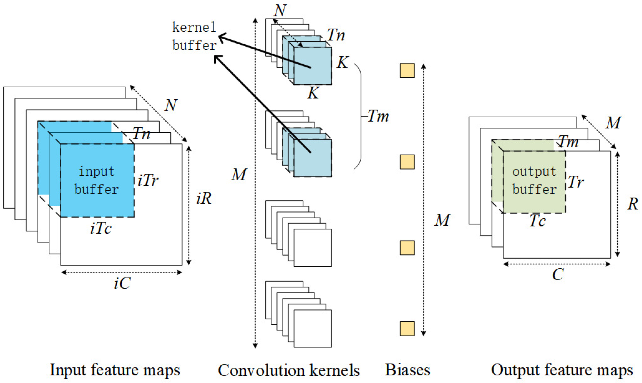
Figure 1 illustrates the process of loop tiling.
N,
, and
represent the number of channels, rows, and columns of the input feature maps, respectively.
M,
R, and
C represent the number of channels, rows, and columns of the output feature maps, respectively.
K represents the height or width of the convolutional kernels.
,
, and
represent the number of rows, columns, and channels of the output feature map tiles, respectively.
,
, and
represent the number of rows, columns, and channels of the input feature map tiles, respectively. In
Figure 1, the blue blocks represent an input feature map tiles. The cyan blocks represent a tile of convolutional kernel weights, and the green blocks represent an output feature map tile obtained through convolution operation. The other parts of the output feature map can be obtained sequentially through the loop process.
For channel-parallel convolutions (such as standard convolutions), NCHW is more advantageous because data across channels is stored contiguously, making it easier to load multiple channels simultaneously. For spatial-parallel convolutions (such as depthwise and separable convolutions), NHWC is preferable since sliding window accesses along the height and width dimensions are more continuous, improving cache hit rates. In DRAM burst transfers, NCHW is better suited for loading multiple channels at once, making it ideal for models with a high number of channels. On the other hand, NHWC is more suitable for sliding accesses along spatial dimensions, optimizing burst read lengths to better match convolution windows, which benefits lightweight models. To better accommodate standard convolutions, this work focuses exclusively on optimizing the NCHW data layout.
For a fixed set of data, there are two DDR4 characters [
8] that result in different access latency values depending on the memory access sequence:
The row buffer hit ratio influences DDR access latency.
Based on the property that each bank can serve different requests separately, the parallelism of the bank is utilized to improve memory access throughput to affect DDR access latency.
Taking the Micron MT40A512M16 model as an example for DDR4, the addressing scheme of MT40A512M16 is illustrated in
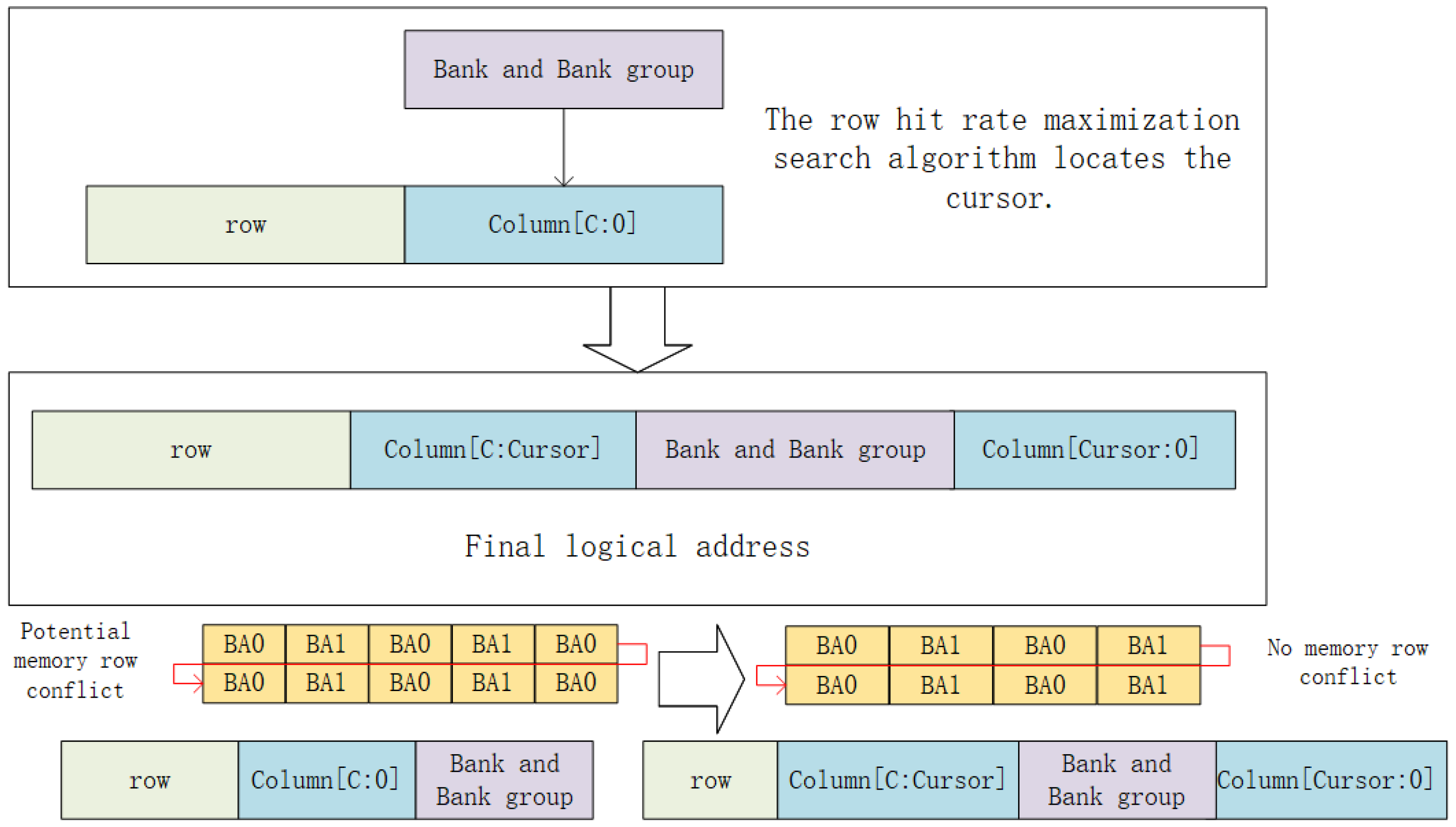
Table 1. According to the characteristics mentioned above, as long as consecutively accessed data are either located in different banks or in the same row within the same bank, no memory row conflicts occur. For ease of analysis, we simplify the bank group configuration and reduce the number of banks to two. The address bits are arranged from MSB to LSB in the order of: Row → Column → Bank.
Figure 2 shows a feature map with 2 channels.
When it serves as the input feature map, the accelerator reads each tile in NCHW order. In this case, two types of memory row conflicts may occur: the first occurs when accessing data across rows within the same channel of a tile, as indicated by process ① in the figure; the second occurs when accessing data from different channels of the tile, as indicated by process ③.
When it serves as the output feature map, the accelerator writes the output feature map in NCHW order. In this case, two types of memory row conflicts may occur: the first occurs when writing data across rows within the same channel of the output feature map, as indicated by process ② in the figure; the second occurs when writing data from different channels of the output feature map, as indicated by process 4.
Table 1.
The addressing scheme of MT40A512M16.
Table 1.
The addressing scheme of MT40A512M16.
| Parameter | Detailed Description |
|---|
| Number of bank groups | 2 |
| Bank group address | BG0 |
| Bank count per group | 4 |
| Bank address in bank group | BA[1:0] |
| Row addressing | 64K (A[15:0]) |
| Column addressing | 1K (A[9:0]) |
| Page size 1 | 2KB |
Figure 2.
A feature map with 2 channels and BA0 indicates data stored in Bank 0.
Figure 2.
A feature map with 2 channels and BA0 indicates data stored in Bank 0.
In
Figure 2, the data involved in processes ①, ②, ③, and ④ come from different banks, illustrating cases where no row conflicts occur. If any two consecutively accessed data items in a process reside in the same bank—such as both being in BA0—a memory row conflict may occur.
4. Proposed Improved Data Layout Strategy
To reduce memory row conflicts arising from the four processes shown in
Figure 2, this paper proposes a method for dynamically adjusting logical addresses. Without considering burst length, using the mapping strategy (Row → Column → Bank and bank group) ensures that consecutive data in a feature map row are distributed across different banks. With the mapping strategy (Row → Column[C:Cursor] → Bank and bank group → Column[Cursor:0]), every
data entries are placed in the same row of the same bank, which also avoids memory row conflicts. Since the number of memory accesses and their addresses throughout the CNN inference process can be determined beforehand, and the row hit rate under the current address mapping strategy can be statistically evaluated, we determine the Cursor value for each layer’s feature map before inference begins. In Algorithm 1, an exhaustive search is employed to determine the Cursor value for each of the
n convolutional layers. As shown in
Figure 3, after applying Algorithm 1, an address mapping strategy tailored to the current feature map can be obtained, effectively reducing the probability of memory access row conflicts.
| Algorithm 1: Row hit rate maximization search algorithm |
![Electronics 14 02127 i001]() |
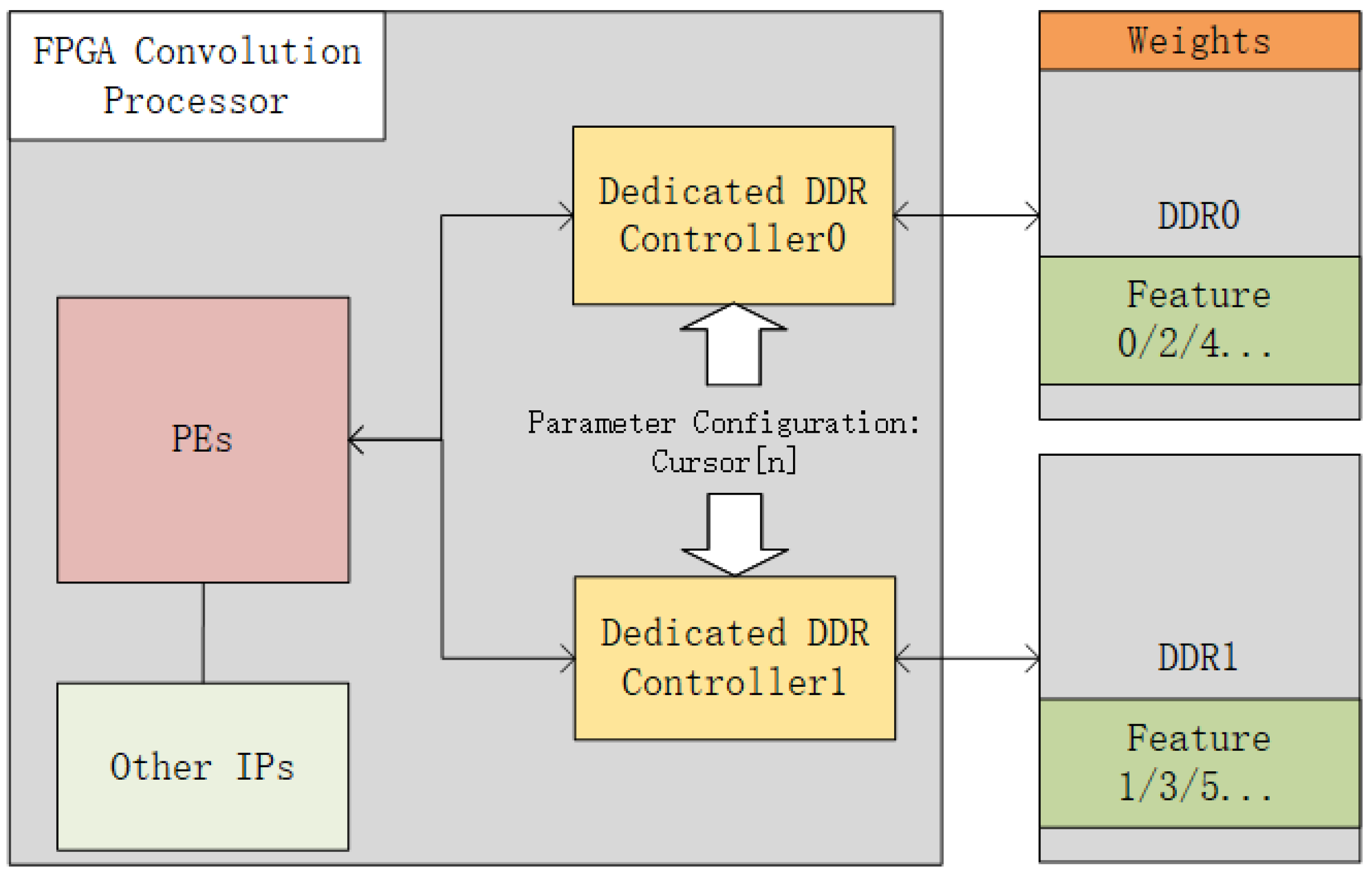
Since each layer’s feature map has a dedicated address mapping strategy, storing two adjacent layers in the same DDR may lead to data storage conflicts. To prevent this issue, this work adopts two DDRs with independent address spaces: while one DDR reads the feature map, the other writes the next layer’s feature map. This alternating access pattern enables seamless execution of the CNN inference task. As shown in
Figure 4, the convolution processor connects to two DDR4 memory modules with independent address buses. Specifically, DDR0 stores weight data, while both DDR0 and DDR1 are used to store input and output feature map data. The two DDR modules operate in parallel. When DDR0 stores input feature maps and DDR1 is prepared to store output feature maps, the processing elements (PEs) simultaneously read weights and input feature map data from DDR0, while storing computed results (output feature maps) in DDR1. Conversely, when DDR0 is prepared to store output feature maps and DDR1 stores input feature maps, the PEs read weights and input feature map data in parallel from DDR0 and DDR1, respectively, while storing the results (output feature maps) back into DDR0.
The proposed dynamic address mapping approach is designed to be compatible with a wide range of DDR memory standards, including DDR3, DDR4, and DDR5. This compatibility is achieved by abstracting the address mapping logic from specific hardware parameters, allowing it to adapt dynamically based on the memory system’s configuration. Parameters such as clock frequency, data rate, pin count, and ECC (Error Correction Code) are treated as configurable inputs during system initialization. For instance, the controller can adjust timing constraints (e.g., tRC, tRCD, tRP) according to the target DDR specification to ensure correct scheduling and access latency calculation. Furthermore, the address mapping logic operates at the logical level, meaning it is agnostic to physical data bus width or ECC presence, as long as the underlying memory controller abstracts these details appropriately. This design ensures that the optimization algorithm and hardware controller can be seamlessly integrated into platforms using different DDR standards, enabling broader deployment across various hardware targets.
5. Experimental Results
This section presents both simulation and hardware platform experiments to validate the proposed dynamic memory mapping strategy. We begin with simulation-based memory access analysis using widely adopted CNN models. Then, we validate the proposed accelerator on a real FPGA platform. To ensure reproducibility, we explicitly describe the methodology, datasets, and benchmark configurations. We also compare our method with state-of-the-art tools, such as Vitis AI.
5.1. Simulation Experiments
To evaluate memory row conflict rates, we use the SystemC simulation framework with a custom DDR4-3200 (8-bank) memory model. The simulations are based on convolutional layers extracted from three widely used CNNs: YOLOv2, AlexNet, and VGG16. The network structures are consistent with publicly available implementations from the Darknet and Caffe Model Zoo. The input datasets used to generate feature maps for simulation are sampled from the ImageNet ILSVRC 2012 validation set and the Pascal VOC 2007 dataset, both of which are widely recognized benchmarks in the computer vision community. Each model processes a batch of 16 input images, resized to the native input resolution of the respective network (e.g., 224 × 224 for AlexNet and VGG16, 416 × 416 for YOLOv2). Feature maps and intermediate layer outputs are dumped from the original models and used to feed the SystemC simulation framework. This ensures that the memory access traces are derived from realistic and representative workloads. The experimental validation is performed using SystemC-based simulation, and the data bit-width is 32-bit floating point.
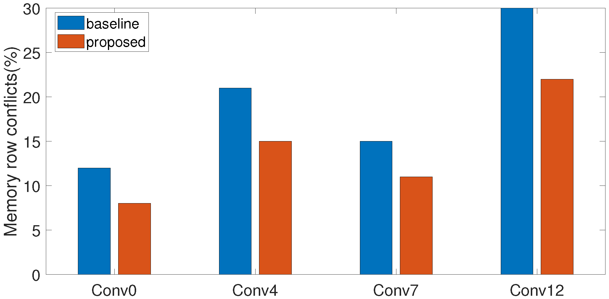
The baseline address mapping follows a conventional format where physical address bits are ordered as Row → Column → Bank. As shown in
Figure 5,
Figure 6 and
Figure 7, simulations reveal varying row conflict characteristics across the models: YOLOv2 suffers up to 30% conflict at Conv12 due to high channel concurrency and small feature maps. VGG16 shows 34% conflict at Conv9 due to consecutive 3 × 3 convolutions, while AlexNet exhibits 38% conflict at Conv3, related to mixed kernel sizes.
After applying our optimized address mapping strategy, the peak conflict rates reduce to 22%, 23%, and 17% for YOLOv2, VGG16, and AlexNet, respectively. This validates the generality of our method under varying kernel sizes (3 × 3–5 × 5), channel counts (256–512), and spatial resolutions (7 × 7–56 × 56), while fully respecting DDR4 timing constraints (tRC = 45 ns, tRCD = 13.75 ns) and the 8-bank architecture.
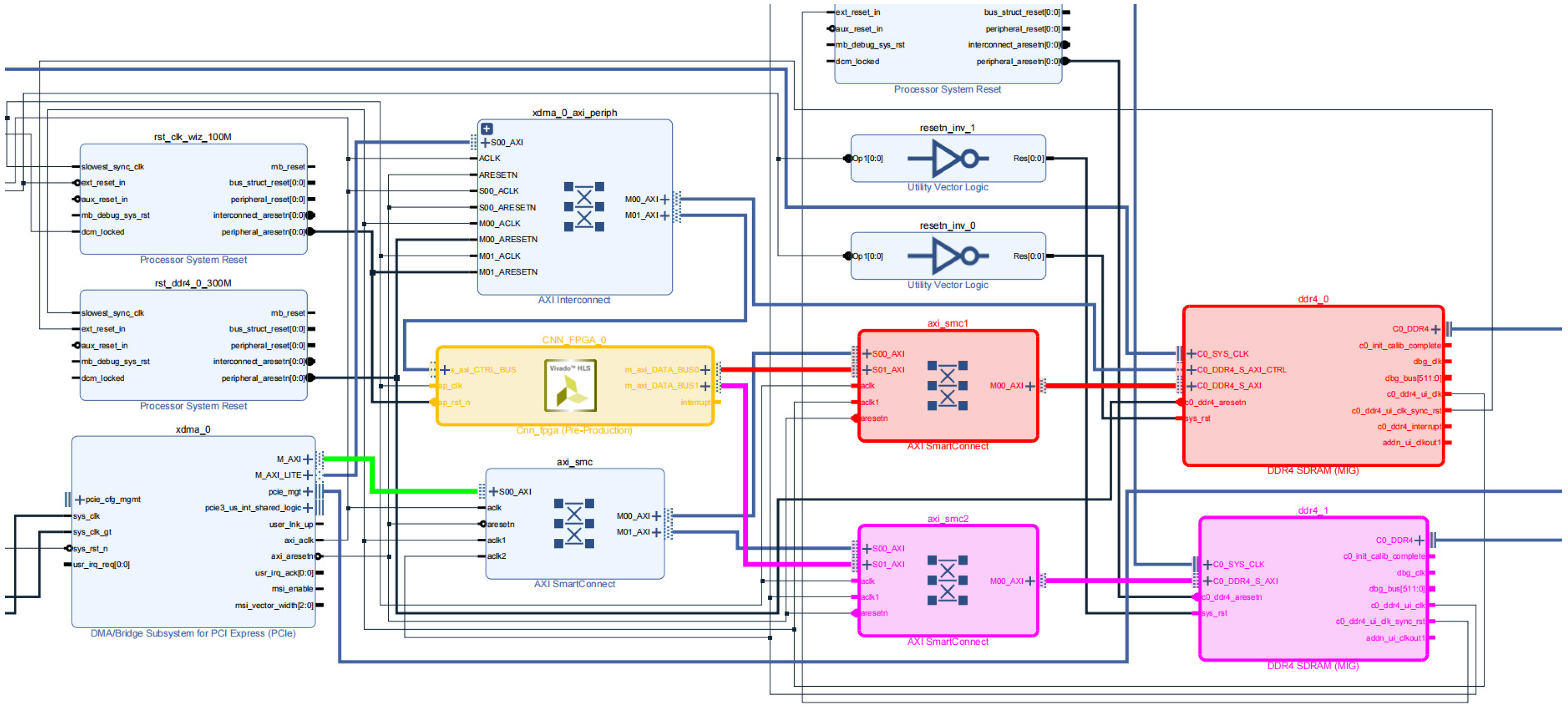
5.2. Platform Experiments
We deploy the proposed accelerator design on the Xilinx KCU1500 FPGA board (Xilinx/AMD, San Jose/Santa Clara, CA, USA). The accelerator is implemented using Vivado HLS 2019.1 and integrated via the Vivado IP Integrator. The board features four independent DDR4 modules; in this study, two are configured with our dynamic address mapping controllers (
Figure 8).
To ensure a fair comparison, the same network structures (YOLOv2, VGG16, AlexNet) are compiled using Vitis AI [
24] and oneDNN [
17] with their default quantization and scheduling parameters. Our accelerator executes these models using identical weights and input data derived from pretrained ImageNet and VOC variants. Specifically, all inputs are preprocessed using the same pipeline as in the original model training. For YOLOv2, images from VOC 2007 are resized and normalized according to the official Darknet preprocessing routine. For AlexNet and VGG16, images from ImageNet are center-cropped to 224 × 224 and normalized using the mean and standard deviation values reported in the Caffe Model Zoo. The datasets are chosen not only for their prevalence in benchmarking but also for their diversity in spatial and channel dimensions, which enables a robust evaluation of the proposed memory mapping scheme under various memory access patterns. In addition to that, the frequency is uniformly set to 100 MHz, and computations are performed using 32-bit floating point.
The latency and throughput results in
Table 2 highlight consistent improvements over Vitis AI, with speedups of 1.12×–1.17×. These gains reflect better memory efficiency and reduced row conflicts, particularly in deep models like VGG16.
Table 3 confirms the accelerator’s efficient use of resources, with all utilization metrics well below 25%, indicating potential for further scaling or multi-instance deployment on mid-range FPGAs.
6. Conclusions
This work proposes a DDR controller for multi-memory FPGA-based convolution accelerators that enhances memory utilization efficiency and reduces row conflict rates. The controller utilizes a novel data placement strategy to coordinate feature map allocation across memory banks. Experimental results demonstrate a 21% reduction in row conflict rate and a 17% throughput improvement in FPGA implementations. The proposed methodology is extensible to various convolutional accelerator architectures and supports arbitrary DDR memory standards, thus enabling notable performance improvements in convolutional operations. However, the current design is primarily evaluated in the context of single-port memory controllers and a specific data layout (NCHW). The scalability of the approach to multi-port memory controller solutions remains an open question, particularly regarding potential increases in control logic complexity and inter-bank coordination overhead. Additionally, it is unclear whether the observed performance gains would persist under more complex memory access patterns and diverse accelerator configurations. Future work will explore lightweight controller variants, support for additional data layout formats, and the potential for deployment on heterogeneous platforms such as GPUs and TPUs. Investigating the effectiveness of the proposed strategy in multi-port and high-bandwidth memory scenarios will also be a key focus.
Author Contributions
Methodology, Y.W. and H.Z.; Software, Y.W.; Formal analysis, Y.W.; Writing—original draft, Y.W.; Writing—review & editing, H.Z. All authors have read and agreed to the published version of the manuscript.
Funding
This research was funded by the Key Laboratory of Artificial Intelligence, Ministry of Education, ShangHai JiaoTong University (Number of Open Project Program of Key Laboratory of Artificial Intelligence, Ministry of Education: AI202106) and the National Key Research and Development Program under Grant 2022YFB3303700.
Data Availability Statement
The data presented in this study are available on request from the corresponding author.
Conflicts of Interest
The authors declare no conflicts of interest.
References
- Chilimbi, T.; Suzue, Y.; Apacible, J.; Kalyanaraman, K. Project Adam: Building an Efficient and Scalable Deep Learning Training System. In Proceedings of the 11th USENIX Conference on Operating Systems Design and Implementation, Broomfield, CO, USA, 6–8 October 2014; OSDI’14. pp. 571–582. [Google Scholar]
- Coates, A.; Huval, B.; Wang, T.; Wu, D.J.; Ng, A.Y.; Catanzaro, B. Deep Learning with COTS HPC Systems. In Proceedings of the 30th International Conference on International Conference on Machine Learning, Atlanta, GA, USA, 16–21 June 2013; ICML’13. Volume 28, pp. III-1337–III-1345. [Google Scholar]
- Zhou, X.; Du, Z.; Zhang, S.; Zhang, L.; Lan, H.; Liu, S.; Li, L.; Guo, Q.; Chen, T.; Chen, Y. Addressing Sparsity in Deep Neural Networks. IEEE Trans. Comput. Aided Des. Integr. Circuits Syst. 2019, 38, 1858–1871. [Google Scholar] [CrossRef]
- Lavin, A.; Gray, S. Fast Algorithms for Convolutional Neural Networks. In Proceedings of the 2016 IEEE Conference on Computer Vision and Pattern Recognition (CVPR), Las Vegas, NV, USA, 27–30 June 2016; pp. 4013–4021. [Google Scholar] [CrossRef]
- Liu, X.Y.; Hong, H.; Zhang, Z.; Tong, W.; Kossaifi, J.; Wang, X.; Walid, A. High-Performance Tensor-Train Primitives Using GPU Tensor Cores. IEEE Trans. Comput. 2024, 73, 2634–2648. [Google Scholar] [CrossRef]
- Nada, A.; Sarda, G.M.; Lenormand, E. Cooperative Warp Execution in Tensor Core for RISC-V GPGPU. In Proceedings of the 2025 IEEE International Symposium on High Performance Computer Architecture (HPCA), Las Vegas, NV, USA, 1–5 March 2025; pp. 1422–1436. [Google Scholar] [CrossRef]
- Chen, Y.H.; Yang, T.J.; Emer, J.; Sze, V. Eyeriss v2: A Flexible Accelerator for Emerging Deep Neural Networks on Mobile Devices. IEEE J. Emerg. Sel. Top. Circuits Syst. 2019, 9, 292–308. [Google Scholar] [CrossRef]
- Li, X.; Yuan, Z.; Guan, Y.; Sun, G.; Zhang, T.; Wei, R.; Niu, D. Flatfish: A Reinforcement Learning Approach for Application-Aware Address Mapping. IEEE Trans. Comput. Aided Des. Integr. Circuits Syst. 2022, 41, 4758–4770. [Google Scholar] [CrossRef]
- Chen, X.; Chen, J.; Chen, D.Z.; Hu, X.S. Optimizing memory efficiency for convolution kernels on kepler GPUs. In Proceedings of the 2017 54th ACM/EDAC/IEEE Design Automation Conference (DAC), Austin, TX, USA, 18–22 June 2017; pp. 1–6. [Google Scholar] [CrossRef]
- Chellapilla, K.; Puri, S.; Simard, P.Y. High Performance Convolutional Neural Networks for Document Processing. In Tenth International Workshop on Frontiers in Handwriting Recognition; Suvisoft: Tampre, Finland, 2006. [Google Scholar]
- Chen, T.; Moreau, T.; Jiang, Z.; Zheng, L.; Yan, E.; Cowan, M.; Shen, H.; Wang, L.; Hu, Y.; Ceze, L.; et al. TVM: An automated end-to-end optimizing compiler for deep learning. In Proceedings of the 13th USENIX Conference on Operating Systems Design and Implementation, USA, Carlsbad, CA, USA, 8–10 October 2018; OSDI’18. pp. 579–594. [Google Scholar]
- Chi, L.; Jiang, B.; Mu, Y. Fast Fourier Convolution. In Advances in Neural Information Processing Systems; Larochelle, H., Ranzato, M., Hadsell, R., Balcan, M., Lin, H., Eds.; Curran Associates, Inc.: Red Hook, NY, USA, 2020; Volume 33, pp. 4479–4488. [Google Scholar]
- Chetlur, S.; Woolley, C.; Vandermersch, P.; Cohen, J.; Tran, J.; Catanzaro, B.; Shelhamer, E. cuDNN: Efficient Primitives for Deep Learning. arXiv 2014, arXiv:1410.0759. [Google Scholar]
- Jia, Y.; Shelhamer, E.; Donahue, J.; Karayev, S.; Long, J.; Girshick, R.; Guadarrama, S.; Darrell, T. Caffe: Convolutional Architecture for Fast Feature Embedding. In Proceedings of the 22nd ACM International Conference on Multimedia, Orlando, FL, USA, 3–7 November 2014; MM’14. pp. 675–678. [Google Scholar] [CrossRef]
- Peemen, M.; Setio, A.A.A.; Mesman, B.; Corporaal, H. Memory-centric accelerator design for Convolutional Neural Networks. In Proceedings of the 2013 IEEE 31st International Conference on Computer Design (ICCD), Asheville, NC, USA, 6–9 October 2013; pp. 13–19. [Google Scholar] [CrossRef]
- Han, S.; Mao, H.; Dally, W.J. Deep Compression: Compressing Deep Neural Networks with Pruning, Trained Quantization and Huffman Coding. arXiv 2016, arXiv:1510.00149. [Google Scholar]
- Li, J.; Qin, Z.; Mei, Y.; Cui, J.; Song, Y.; Chen, C.; Zhang, Y.; Du, L.; Cheng, X.; Jin, B.; et al. oneDNN Graph Compiler: A Hybrid Approach for High-Performance Deep Learning Compilation. In Proceedings of the 2024 IEEE/ACM International Symposium on Code Generation and Optimization (CGO), Edinburgh, UK, 2–6 March 2024. [Google Scholar]
- Ragan-Kelley, J.; Barnes, C.; Adams, A.; Paris, S.; Durand, F.; Amarasinghe, S. Halide: A language and compiler for optimizing parallelism, locality, and recomputation in image processing pipelines. SIGPLAN Not. 2013, 48, 519–530. [Google Scholar] [CrossRef]
- Howard, A.G.; Zhu, M.; Chen, B.; Kalenichenko, D.; Wang, W.; Weyand, T.; Andreetto, M.; Adam, H. MobileNets: Efficient Convolutional Neural Networks for Mobile Vision Applications. arXiv 2017, arXiv:1704.04861. [Google Scholar]
- Alwani, M.; Chen, H.; Ferdman, M.; Milder, P. Fused-layer CNN accelerators. In Proceedings of the 2016 49th Annual IEEE/ACM International Symposium on Microarchitecture (MICRO), Taipei, China, 15–19 October 2016; pp. 1–12. [Google Scholar] [CrossRef]
- Long, X.; Gong, X.; Zhang, B.; Zhou, H. Deep learning based data prefetching in CPU-GPU unified virtual memory. J. Parallel Distrib. Comput. 2023, 174, 19–31. [Google Scholar] [CrossRef]
- ARM. Learn the Architecture Introducing Neon. Available online: https://developer.arm.com/documentation/102474/0100/?lang=en (accessed on 20 May 2025).
- Xilinx/AMD, San Jose/Santa Clara, California, USA. Vitis AI User Guide: AI Inference Development. 2020. Available online: https://docs.xilinx.com/r/en-US/ug1414-vitis-ai (accessed on 13 May 2025).
- Xilinx/AMD, San Jose/Santa Clara, California, USA. Vitis AI Model Zoo. 2021. Available online: https://github.com/Xilinx/Vitis-AI/tree/master/model_zoo (accessed on 13 May 2025).
- Li, M.; Liu, Y.; Liu, X.; Sun, Q.; You, X.; Yang, H.; Luan, Z.; Gan, L.; Yang, G.; Qian, D. The Deep Learning Compiler: A Comprehensive Survey. IEEE Trans. Parallel Distrib. Syst. 2021, 32, 708–727. [Google Scholar] [CrossRef]
- Zheng, L.; Jia, C.; Sun, M.; Wu, Z.; Yu, C.H.; Haj-Ali, A.; Wang, Y.; Yang, J.; Zhuo, D.; Sen, K.; et al. Ansor: Generating high-performance tensor programs for deep learning. In Proceedings of the 14th USENIX Conference on Operating Systems Design and Implementation, Online, 4–6 November 2020. OSDI’20. [Google Scholar]
- Vasilache, N.; Zinenko, O.; Theodoridis, T.; Goyal, P.; DeVito, Z.; Moses, W.S.; Verdoolaege, S.; Adams, A.; Cohen, A. Tensor Comprehensions: Framework-Agnostic High-Performance Machine Learning Abstractions. arXiv 2018, arXiv:1802.04730. [Google Scholar]
- Xu, R.; Guo, M.; Wang, J.; Li, X.; Zhou, B.; Loy, C.C. Texture Memory-Augmented Deep Patch-Based Image Inpainting. IEEE Trans. Image Process. 2021, 30, 9112–9124. [Google Scholar] [CrossRef] [PubMed]
- Intel. OpenVINO 2025.1. Available online: https://docs.openvino.ai/2025/index.html (accessed on 20 May 2025).
- Ma, Y.; Cao, Y.; Vrudhula, S.; Seo, J.s. Optimizing the Convolution Operation to Accelerate Deep Neural Networks on FPGA. IEEE Trans. Very Large Scale Integr. Syst. 2018, 26, 1354–1367. [Google Scholar] [CrossRef]
| Disclaimer/Publisher’s Note: The statements, opinions and data contained in all publications are solely those of the individual author(s) and contributor(s) and not of MDPI and/or the editor(s). MDPI and/or the editor(s) disclaim responsibility for any injury to people or property resulting from any ideas, methods, instructions or products referred to in the content. |
© 2025 by the authors. Licensee MDPI, Basel, Switzerland. This article is an open access article distributed under the terms and conditions of the Creative Commons Attribution (CC BY) license (https://creativecommons.org/licenses/by/4.0/).


