1. Introduction
Millimeter-wave frequencies, including the Ka and K bands, are widely used in 5G communications, satellite communications, and automotive radar applications. For phased array systems operating at millimeter-wave frequencies, power dividers and power combiners are pivotal components, especially in beam-forming integrated circuits (BFICs) and systems that require numerous power dividers/combiners [
1]. The two-way power divider/combiner enables equal-phase power division/combination, inherent port impedance matching, and enhanced isolation between output ports. The operational characteristics of power dividers are governed exclusively by the impedance-transforming/power-combining network design within the structure. The millimeter-wave power divider design needs include several key requirements: minimized input/output reflection coefficients, low insertion loss characteristics, good isolation between output ports, small amplitude imbalance and phase difference, and compact physical dimensions for system integration. Significant research efforts have been devoted to optimizing power divider performance.
The primary design objective for chip-on-chip (CoC) integration is miniaturization. The λ/4 transmission line in traditional Wilkinson power dividers is space-intensive and poses challenges for integration. In BFICs integrating numerous VAP (variable amplitude and phase) channels, compact circuit block designs are essential to minimize the overall integrated area and mitigate crosstalk among channels. To improve integration, lumped-element networks have been validated as viable replacements for distributed transmission lines in miniaturized designs [
2,
3,
4,
5,
6,
7,
8]. Representative implementations include π-section lumped networks [
2], L-section lumped networks [
3], and bridged T-coil networks [
4,
5], which replace quarter-wavelength lines. Additionally, transformer-based Wilkinson architectures have demonstrated monolithic integration capability while maintaining impedance-matching characteristics [
8].
Furthermore, since the system requires cascading multiple stages of power combiners, minimizing insertion loss becomes critical for maintaining overall system performance, including gain and power efficiency. For example, researchers propose a design method for a single-stage high-performance lumped distributed Wilkinson power divider [
9]. Although the single-stage power divider achieves low insertion loss, its operational bandwidth remains limited. In integrated circuit implementations, multi-stage topologies are most effective for achieving both wide bandwidth and high isolation. Consequently, multi-stage matching circuits are commonly employed in broadband designs [
10,
11,
12,
13]. Specifically, a broadband lumped-element power divider with a multi-section LC-ladder circuit and a single isolation resistor, achieving over 100% fractional bandwidth in the VHF band [
11]. Moreover, for power dividers with fully symmetrical circuit structures, excellent amplitude balance and minimal phase error between output ports are inherently achievable [
14,
15,
16,
17].
The high inter-port isolation minimizes mutual signal interference, preserving output signal integrity. Enhanced port isolation can be achieved through optimization of the isolation network topology. For instance, the optimal placement of three isolation resistors in coupled-line Wilkinson power dividers has been systematically analyzed [
18]. Moreover, integrated isolation networks have been developed to simultaneously improve input/output return loss and port isolation [
19]. Additionally, the isolation performance of filter-integrated power dividers has been improved by incorporating an RLC network [
20]. In summary, designing a power divider that satisfies good matching, high isolation, low insertion loss, small amplitude imbalance and phase difference, and compact area requirements is highly challenging.
This paper presents a multi-stage lumped element Wilkinson power divider/combiner (WPDC) that utilizes separate impedance matching for even-mode and odd-mode operation. Small component values in the even-mode path ensure low insertion loss and good input matching, while suspended capacitances and resistance in the odd-mode path guarantee excellent output matching and high isolation. In
Section 2, the matching formulas and S-parameter matrices of two traditional single-stage WPDCs are analyzed. Next, a comparison between the π-network topology and the L-network topology is performed through theoretical deduction, evaluating component size and bandwidth performance. Finally, the proposed multi-stage broadband structure is introduced and analyzed. The proposed design requires only a single isolation resistor, simplifying the circuit implementation compared to prior work. Relative to the structure previously reported, the multi-stage wideband WPDC design introduced and analyzed in this paper enables a significant reduction in overall circuit size and insertion loss while maintaining broadband operational capabilities.
Section 3 details a case study of a two-stage WPDC implemented in GlobalFoundries’ 45 nm RFSOI (45RFE) process, including simulation and measured performance results.
2. Theoretical Analysis and Circuit Implementation
2.1. Single-Stage WPDC
In integrated circuit design, the substitution of a quarter-wavelength (λ/4) transmission line with an equivalent lumped element π network can reduce the size [
21].
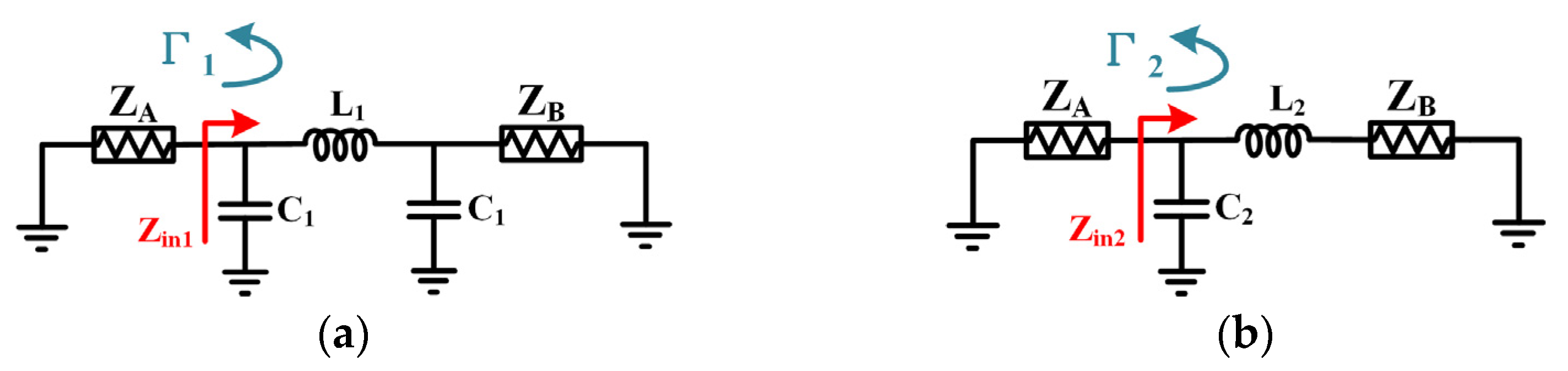
Figure 1 shows two types of single-stage lumped component Wilkinson power dividers. Despite the visual similarity between a Type II WPDC and Type I WPDC, with the exception of one fewer capacitor, their behavior and component values exhibit significant differences.
In a WPDC, the insertion loss is chiefly determined by its even-mode circuit. While the odd-mode matching structure remains consistent across both types of WPDC, the even-mode matching structure varies. The impedance-matching trajectories of π-network matching and L-network matching on the Smith chart reveal that the L network is more straightforward and effective for impedance transformation compared to the π network.
Functioning akin to a λ/4 transmission line facilitates impedance transformation between
Z0 impedance at the split terminals and 2
Z0 impedance at the combined terminal. The π network can be equivalently represented as a cascade of a shunt C/serial L and serial L/shunt C, resulting in an intermediate impedance lower than both
Z0 and 2
Z0, thereby yielding a higher inductance value in the π network than in the L network. Assume that the characteristic impedances of P
1, P
2, and P
3 are
Z0. These component parameters for the two types of WPDC can be readily obtained by conducting odd–even mode analysis. Theoretical analysis conducted by [
22] reveals that
In Equations (1) and (2), Z0 represents the characteristic impedance, while ω0 corresponds to the designed center frequency. The values of inductance and capacitance in a Type II L network are lower than those in a Type I π network by a factor of . Therefore, Type II WPDC offers advantages in terms of component size compared to Type I WPDC.
Through odd–even mode analysis, the
S-parameter matrices for the two types of WPDC can be obtained independently, as indicated by formula (3). The
S-parameter matrices for the two types of WPDC at the center frequency ω
0 indicate that while maintaining identical power division, a Type I WPDC displays a 90° phase shift, whereas a Type II WPDC exhibits a 45° phase shift.
2.2. Component Parameters and Bandwidth
When broader bandwidth is required, adopting a multi-stage WPDC topology becomes crucial. In such cases, the benefits of the L network become more evident especially in terms of optimizing component values and achieving extended bandwidth.
The values of the LC components are highly related to the insertion loss of the lumped-element WPDC in an integrated circuit realization. High-quality factor capacitors can be realized by MIM or MOM capacitors on chip. However, inductors are constructed with spiral windings using metals from the foundry’s back-end-of-line (BEOL) process. Despite their large physical size, on-chip inductors have limited quality factors mainly due to metal loss from limited metal thickness and substrate loss. When considering the self-resonant frequency, an inductor with a smaller inductance value can be designed with a relatively wider metal trace, resulting in a higher-quality factor compared to an inductor with a larger inductance. Consequently, a WPDC designed with lower inductance values not only benefits from a smaller size but also experiences lower insertion loss.
The following analysis compares the component parameters of two networks under identical matching conditions.
Figure 2 illustrate the circuit of the matching from
ZA to
ZB using both π-network topology and L-network topology. The input impedances
Zin1 and
Zin2 as viewed from the load
ZB can be established as
Under the equations of
Zin1 =
ZB and
Zin2 =
ZA, the component parameter formulas for π-network topology and L-network topology matching can be obtained as follows:
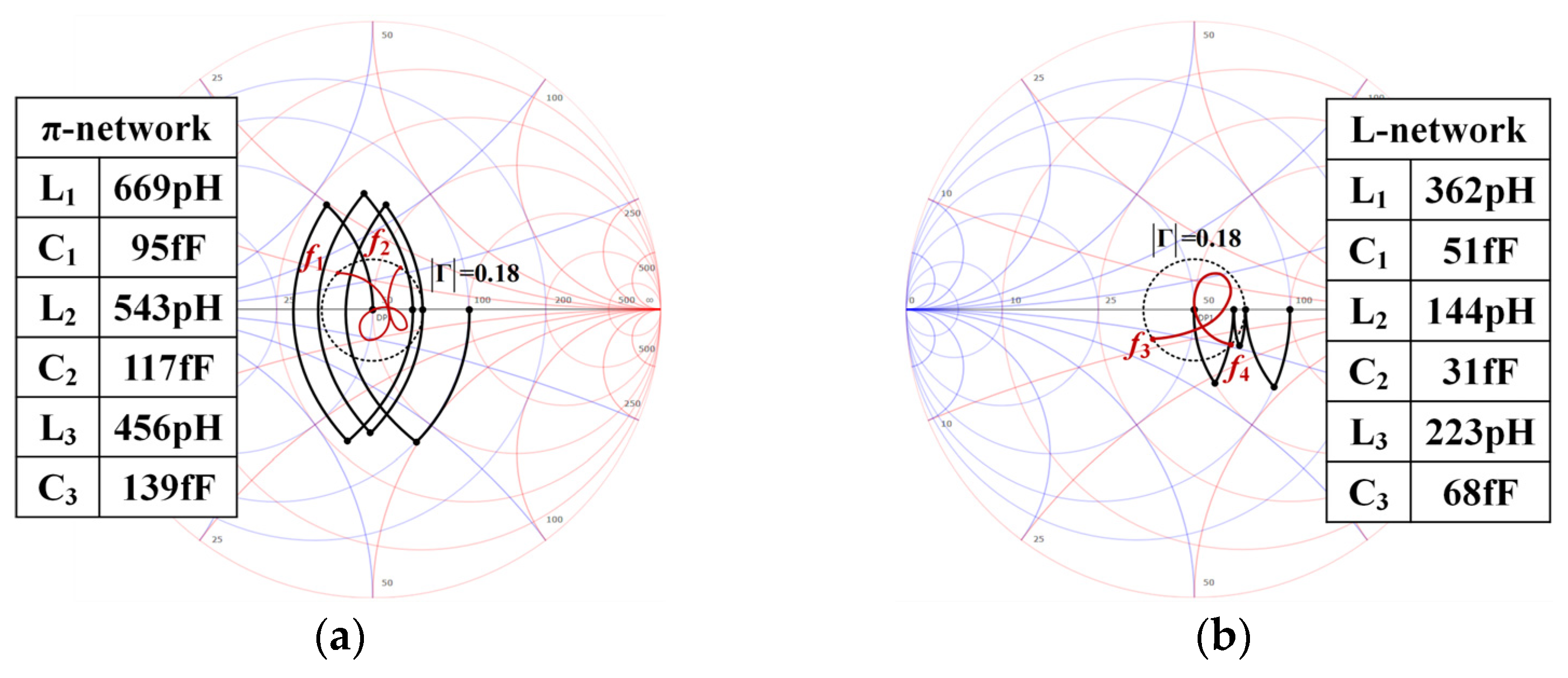
According to the component parameters in the matching formulas, the LC values of the L network are less than those of the π network by a factor of
. With the rise in impedance matching order, the total inductance of the proposed L network is much lower than that of the π network. The theory behind the equation for size reduction can be well proved by the impedance transformation contour shown on the Smith chart (the center frequency
f0 = 20 GHz), as shown in
Figure 3. Moreover, the Smith chart contour also demonstrates that the L-network topology has wider relative impedance-matching bandwidth than the π-network topology. In
Figure 3, the π network can achieve a bandwidth of 12.5 GHz (
f1~
f2) and the L network can achieve a bandwidth of 30.5 GHz (
f3~
f4) within an equal reflection coefficient circle (|Γ = 0.18|), respectively.
In a WPDC design, the component parameter values used to achieve the expected matching conditions perfectly match at the center frequency, but there is still reflection at other frequencies. In
Figure 2, the magnitude of the reflection coefficients |Γ
1| and |Γ
2| at the ports is
If the L-network topology and π-network topology are lossless, the following equations can be obtained:
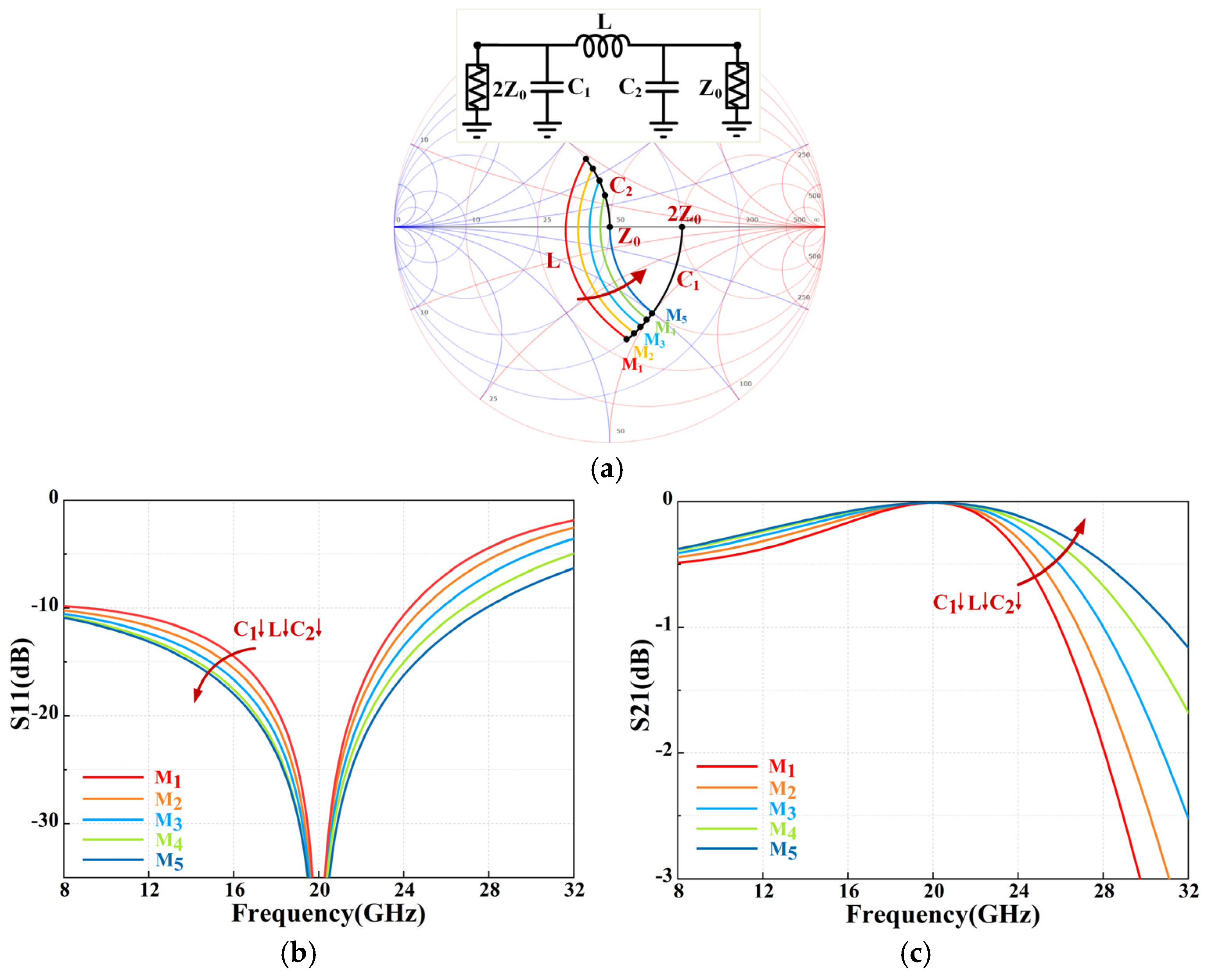
Assuming
ZA = 100 Ω and
ZB = 50 Ω with a center frequency of 20 GHz,
Figure 4 illustrates five parameter modes (M
1–M
5) for the transition from the π network to the L network. As component values change, so do the insertion loss and reflection coefficient. During the transition from the π network to the L network, the bandwidth with S11 < −15 dB progressively increases: 31%, 36%, 42.5%, 48.6%, and finally 52.6%. Among these five matching modes, the L network shows the greatest bandwidth advantage. Thus, the L-network topology offers a wider relative impedance matching bandwidth than the π network.
In conclusion, in the impedance matching from ZA to ZB, the L network’s LC components are smaller than those of the π network and offer a wider return loss bandwidth.
2.3. Multi-Stage WPDC Structure Analysis
Single-stage power dividers typically have narrow bandwidth and only perform optimally (e.g., in return loss and isolation) near the center frequency. In contrast, multi-stage power dividers, by cascading multiple matching network sections, can maintain good matching and isolation across a broader frequency range. To achieve optimal performance, a multi-stage WPDC must be well matched under both even- and odd-mode operating conditions. This ensures excellent input/output return loss and high isolation between output ports. However, the impedance-matching requirements for even-mode and odd-mode are distinct. In even-mode operation, impedance matching is needed from the combined-signal port (2Z0) to the split-signal port (Z0). In contrast, during odd-mode operation, the combined-signal port is short circuited to the ground. The impedance transformation from the low impedance (R/2) at the combined-signal end to the high impedance (Z0) at the split-signal end is crucial with the isolated capacitors and resistor aiding this transition.
The schematic presented in
Figure 5a illustrates the proposed multi-stage lumped-element WPDC structure. The characteristic impedances of P
1, P
2, and P
3 are
Z0. The circuit incorporates a laddered L-network topology (
Figure 5b) to enable impedance transformation from a high impedance (2
Z0) to a low impedance (
Z0) in even mode. Based on the Chebyshev broadband impedance transformation, the values of the inductors and capacitors for each stage can be calculated. In the even-mode circuit, the input impedance Z
e1 and the reflection coefficient Γ
e1 can be expressed as
The input impedance
Ze2 and the reflection coefficient Γ
e2 can be expressed as
For odd-mode analysis, it utilizes a laddered π network (
Figure 5c), which employs the existing L-network topologies from the even-mode design and incorporates supplementary isolation capacitors to match the first isolation resistance impedance (R/2) to a high impedance (
Z0). The design of the isolation capacitor can achieve the odd-mode impedance matching without introducing additional insertion losses. Compared to conventional WPDC designs, the proposed multi-stage WPDC requires only one isolation resistor to achieve the necessary impedance matching for the odd mode while still maintaining excellent isolation performance. In the odd-mode circuit, the input impedance
Zo2 and the reflection coefficient Γ
o2 can be expressed as
By combining the even- and odd-mode analyses, the S-parameter expressions for the WPDC can be obtained as
3. WPDC Design and Results
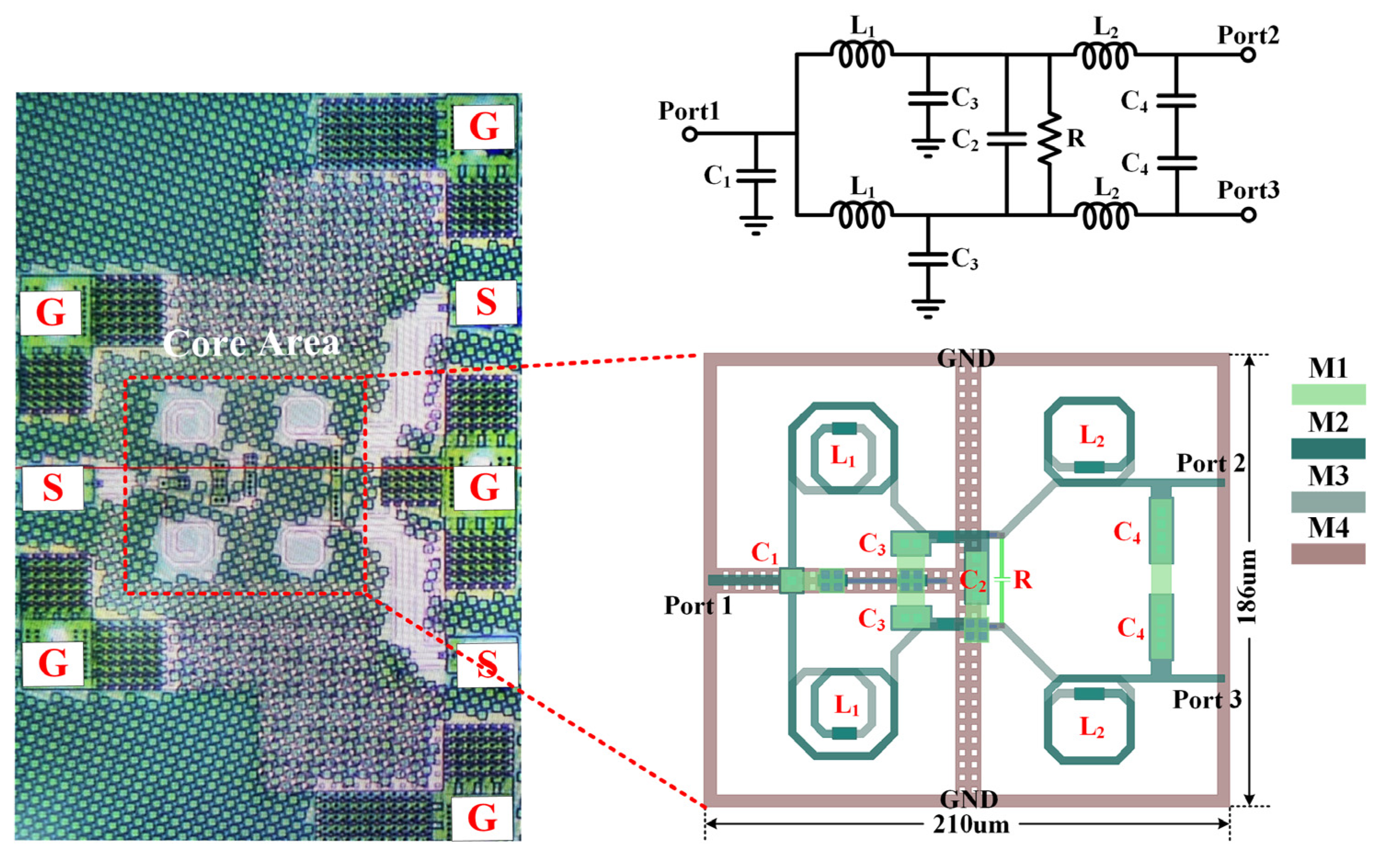
To verify the advantages of this structure, a two-stage Wilkinson power divider/combiner [
23] was designed using GlobalFoundries’ 45RFE process, leveraging the proposed multi-stage WPDC topology. The technology features four metal layers, which are labeled M1 to M4 from top to bottom. The inductors L1 and L2 in the WPDC are fabricated using two layers of 3 μm thick copper metal (M2 and M3) with a line width of 3.5 μm. The grounding signal is routed from metal layer M4 through vias to the pad, while the capacitors were equipped with high-Q metal–insulator–metal caps. It is crucial to consider the electromagnetic coupling and parasitic capacitance between the components and the ground.
The schematic core layout and chip micrograph of the two-stage WPDC are shown in
Figure 6, with a compact core area of only 210 μm × 186 μm, which is only 0.018 λ
0 × 0.016 λ
0 at the center frequency of 26.1 GHz. The WPDC’s Port 1 is connected to the GSG test pad via a 50 Ω transmission line, while Ports 2 and 3 are connected to the GSGSG test pad. Electromagnetic (EM) simulations were performed using the EMX 5.6.1 tool within Cadence software. In the layout, two vertically symmetrical C4 capacitors are used to ensure the symmetry of Port 2 and Port 3, achieving good amplitude balance and minimal phase error. Final layout optimization results indicate the following component values: inductors L
1 = 295 pH and L
2 = 216 pH, capacitors C
1 = 27 fF, C
2 = 60 fF, C
3 = 43 fF, C
4 = 74 fF, and resistance R = 86 Ω.
On-wafer three-port S-parameter measurements were performed using Z40-GSG-150 and Z40-D-GSGSG-150 probes from the Formfactor (Livermore, CA, USA) EPS200MMW probe station together with a Keysight (Santa Rosa, CA, USA) E5080B network analyzer (100 kHz to 53 GHz). Before measurement, a standard four-port SOLT calibration was performed using a ceramic impedance standard substrate (ISS) to eliminate the additional loss of the feed network. Moreover, as the core circuit of the chip is surrounded by a virtual open pad structure, it is necessary to de-embed the pad to ensure the accurate performance of the core circuit.
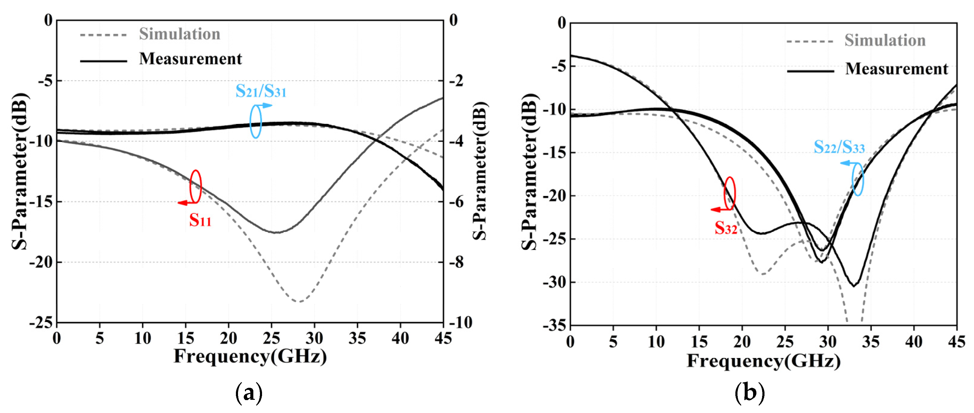
Figure 7a presents the simulated and measured S
11, S
21, and S
31 of the WPDC. Thanks to the circuit’s smaller components, the two-stage WPDC achieves a measured insertion loss of 3.44 dB at 26.1 GHz with insertion loss maintained below 3.8 dB from 0~36 GHz. Moreover, the WPDC achieves measured S
11 below −10 dB from 0 to 37 GHz. This corresponds to a −10 dB matching bandwidth of 37 GHz. Given the design’s center frequency of 26.1 GHz, this results in a fractional bandwidth (FBW) of 141.8%.
Figure 7b presents the simulated and measured S
22, S
33, and S
32 of the WPDC. The measured results are basically consistent with the simulated ones. The WPDC achieves measured S
22/S
33 values below −10 dB from 0 to 42.5 GHz and S
32 below −10 dB from 12 to 42.3 GHz. This corresponds to a −10 dB isolation bandwidth of 30.3 GHz, which is equivalent to a fractional bandwidth (FBW) of 116%.
Within the 12~36 GHz range, the WPDC can simultaneously achieves S
11, S
22, S
33, and S
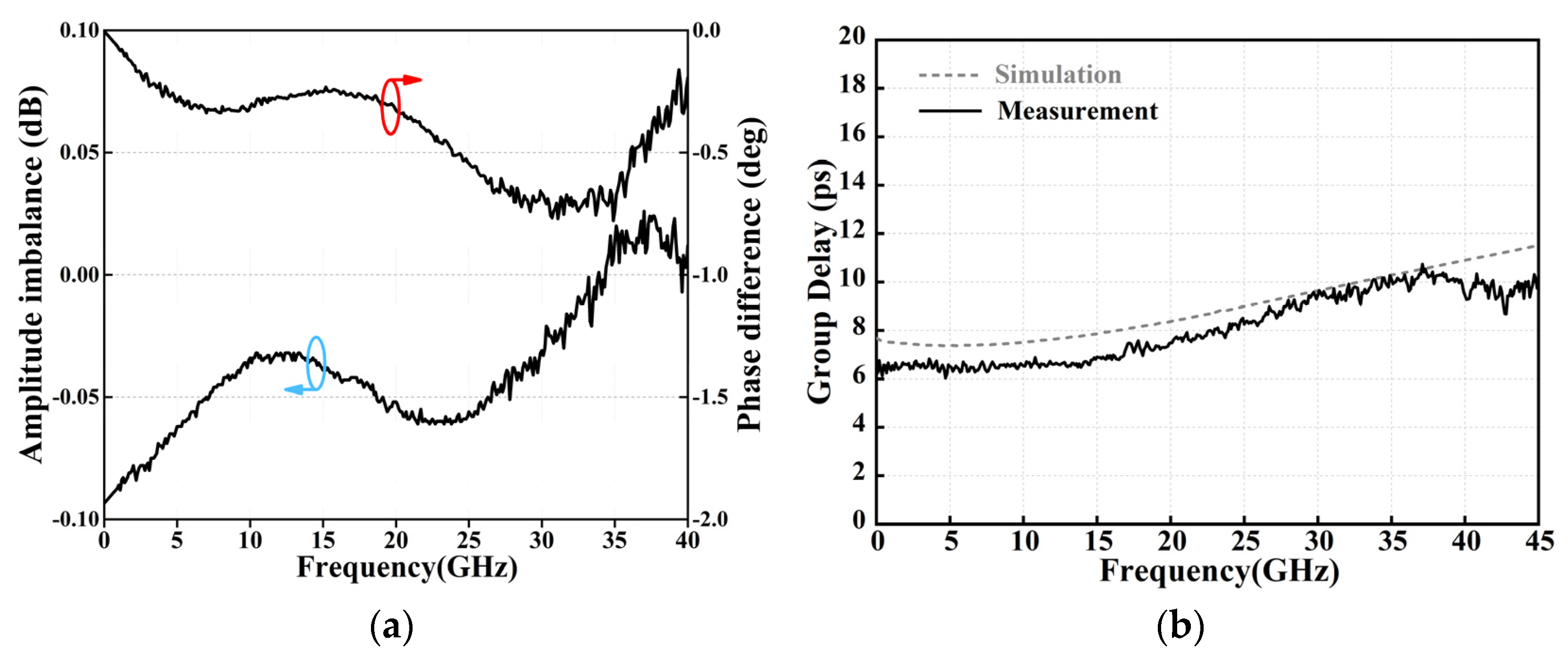
32 measurements smaller than −10 dB, indicating a fractional bandwidth of 100%. Moreover, the amplitude imbalance (AI) and phase difference (PD) of the path from Port 1 to Port 2/Port 3 are illustrated in
Figure 8a, within the 0 to 45 GHz frequency range, the AI measures within 0.09 dB, and the PD is below 0.8 degrees. Additionally, the measured group delays for the signal paths within the same frequency range fall within 8.2 ± 2 ps, as shown in
Figure 8b.
Considering a 12 dB input/output return loss and a 20 dB isolation bandwidth, the measured bandwidth ranges from 18.6 to 33.6 GHz, which is equivalent to a bandwidth of 57.5%, and the in-band insertion loss is less than 0.7 dB. Hence, this power divider circuit exhibits significant potential in the K and Ka bands.
Table 1 summarized the performance of the proposed WPDC along with comparisons with other papers. Compared to other integrated WPDCs, this power divider achieves superior broadband performance in a relatively compact area.
4. Conclusions
This paper introduces a multi-stage WPDC circuit structure that incorporates optimized components for separate even and odd modes. To validate its effectiveness, we fabricated a two-stage WPDC using a commercial 45RFE process. The measurements showed that the insertion loss is below 0.7 dB in the entire band of 18.6 to 33.6 GHz with input and output return losses exceeding 12 dB and isolation levels surpassing 20 dB. Remarkably, the circuit’s size, excluding pads, measures only 0.04 mm2. The two-stage WPDC integrates low insertion loss, excellent return loss, high isolation, compact size, and outstanding amplitude and phase balance. The insertion loss reduction can boost the system gain, subsequently reducing the design complexity of the amplifier in the system. The reduced size of the power divider can directly decrease the space it occupies in phased-array BFICs and systems, enabling more compact system integration and further lowering the overall system cost.


