
Impedance Monitoring of Capacitively Coupled Plasma Based on the Vacuum Variable Capacitor Positions of Impedance Matching Unit


Abstract

1. Introduction
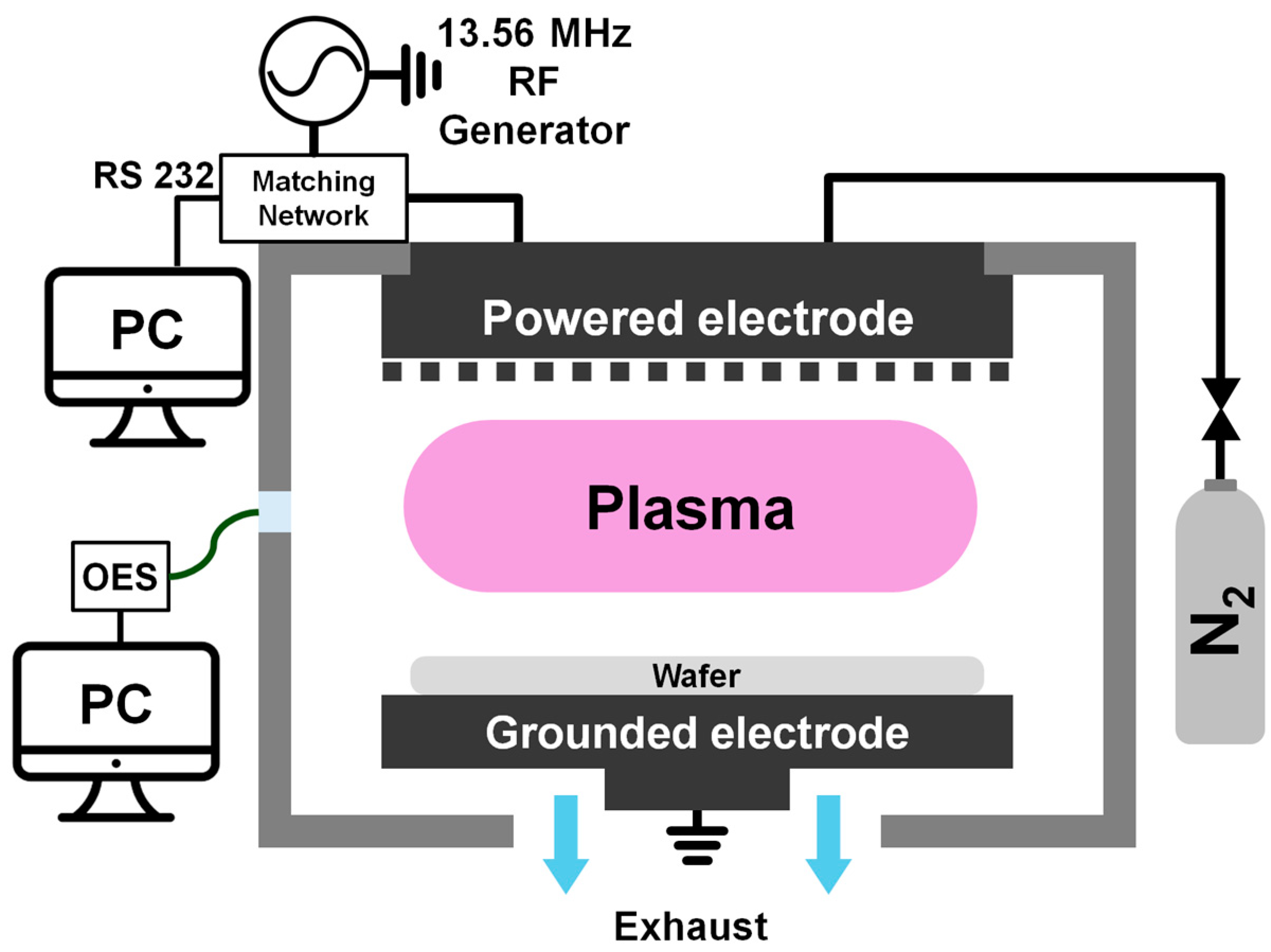
2. Methods
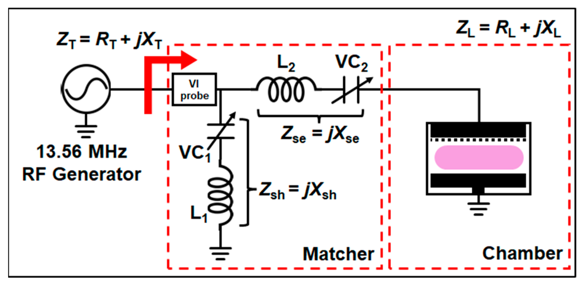
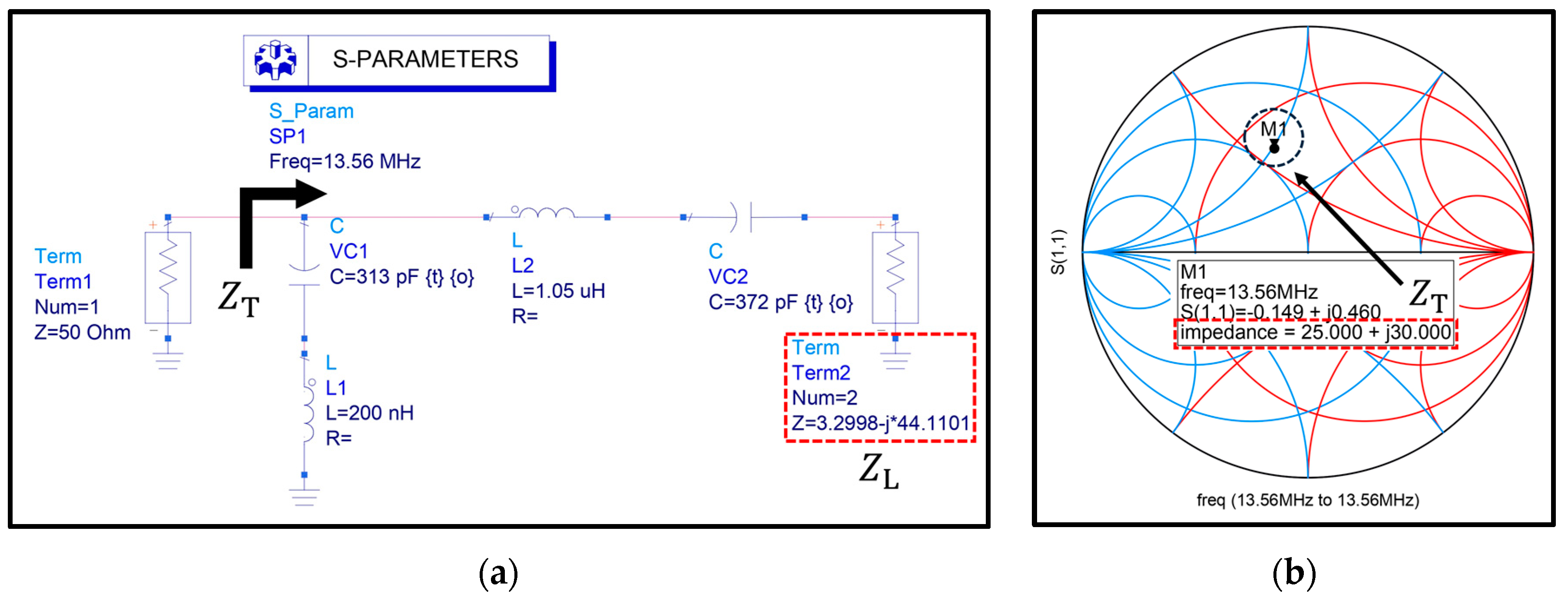
2.1. Derivation of Load Impedance
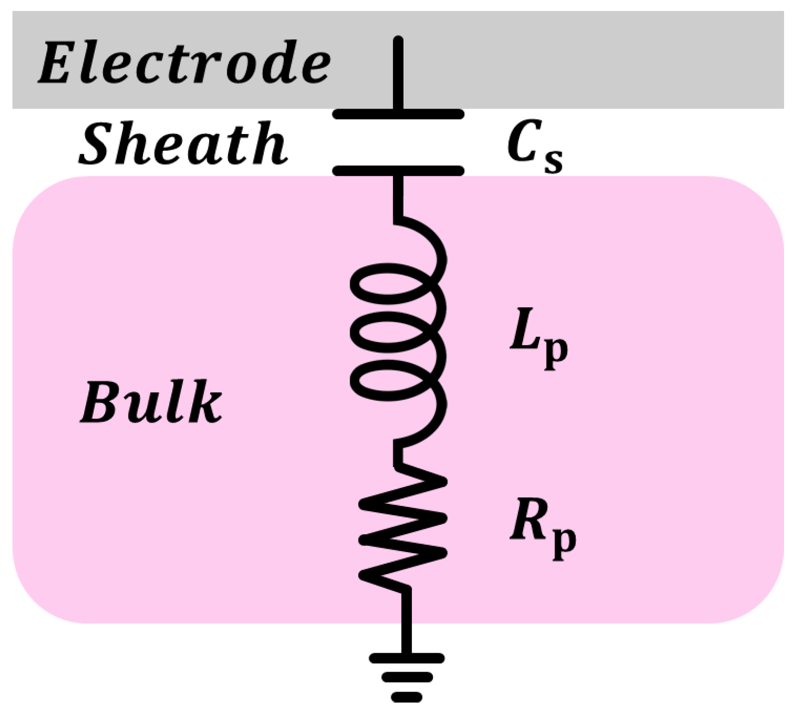
2.2. Equivalent Circuit of Capacitively Coupled Plasma
3. Validation Experiment
4. Result and Discussions
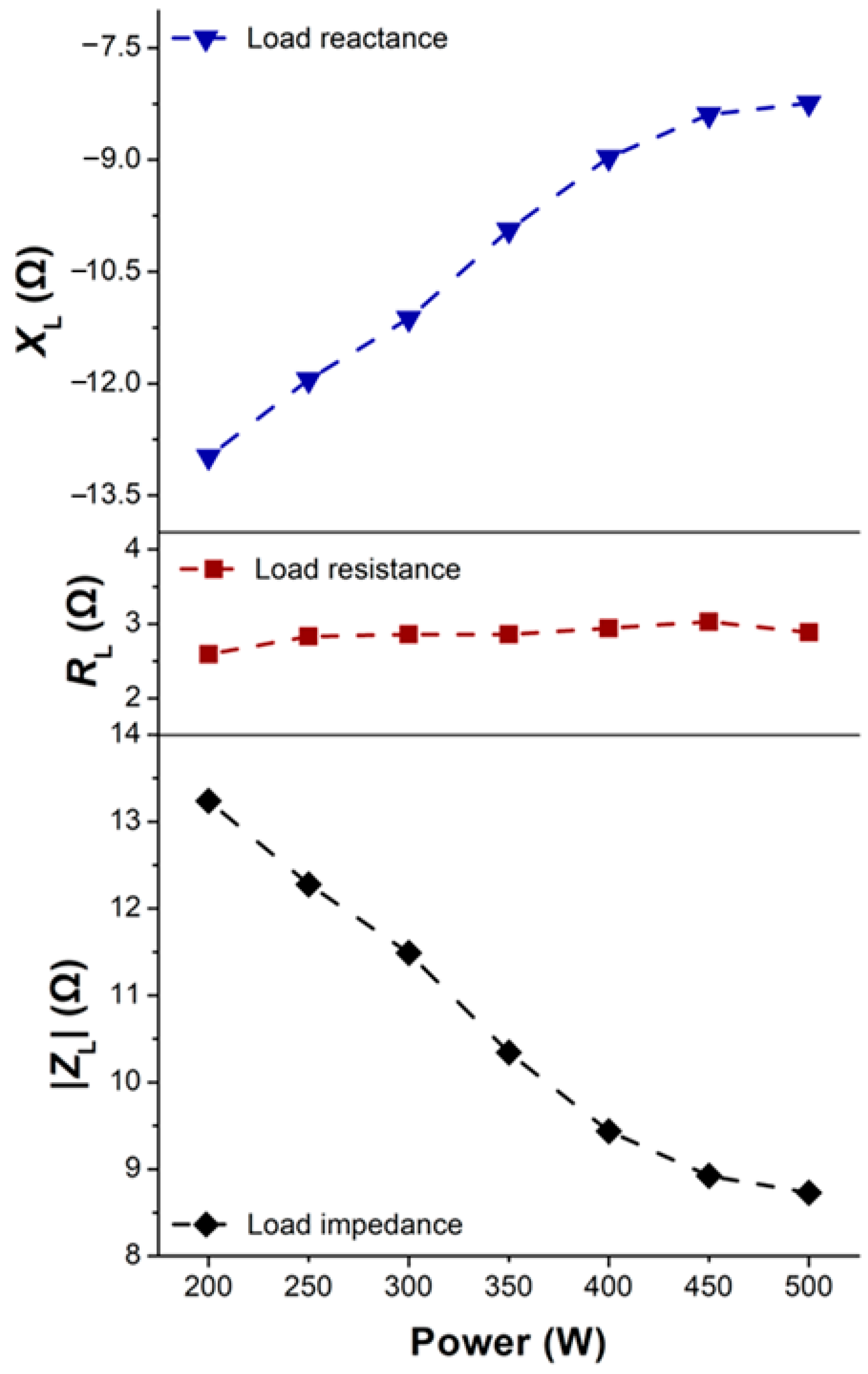
4.1. Result of Power Split Test and Discussion
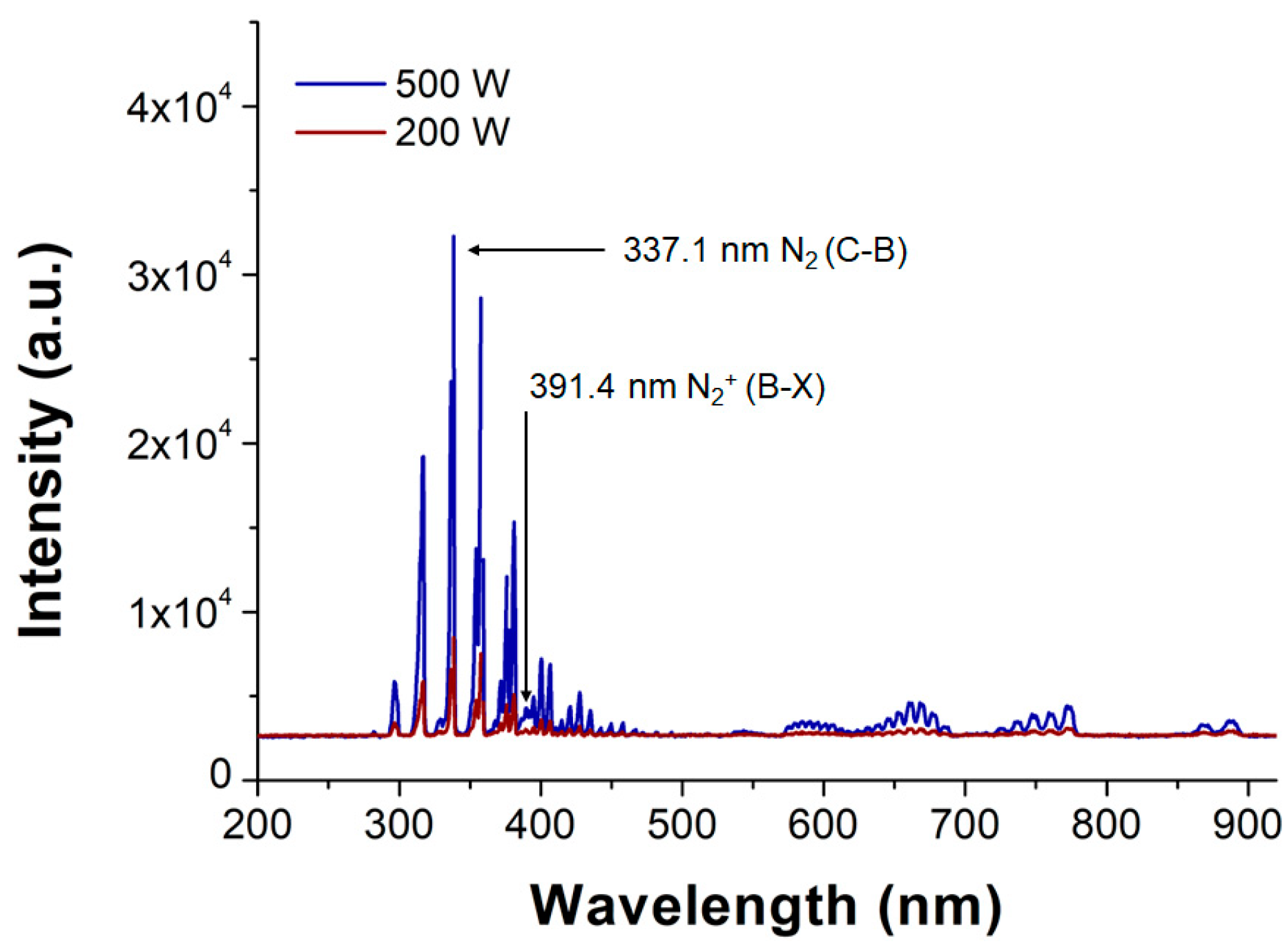
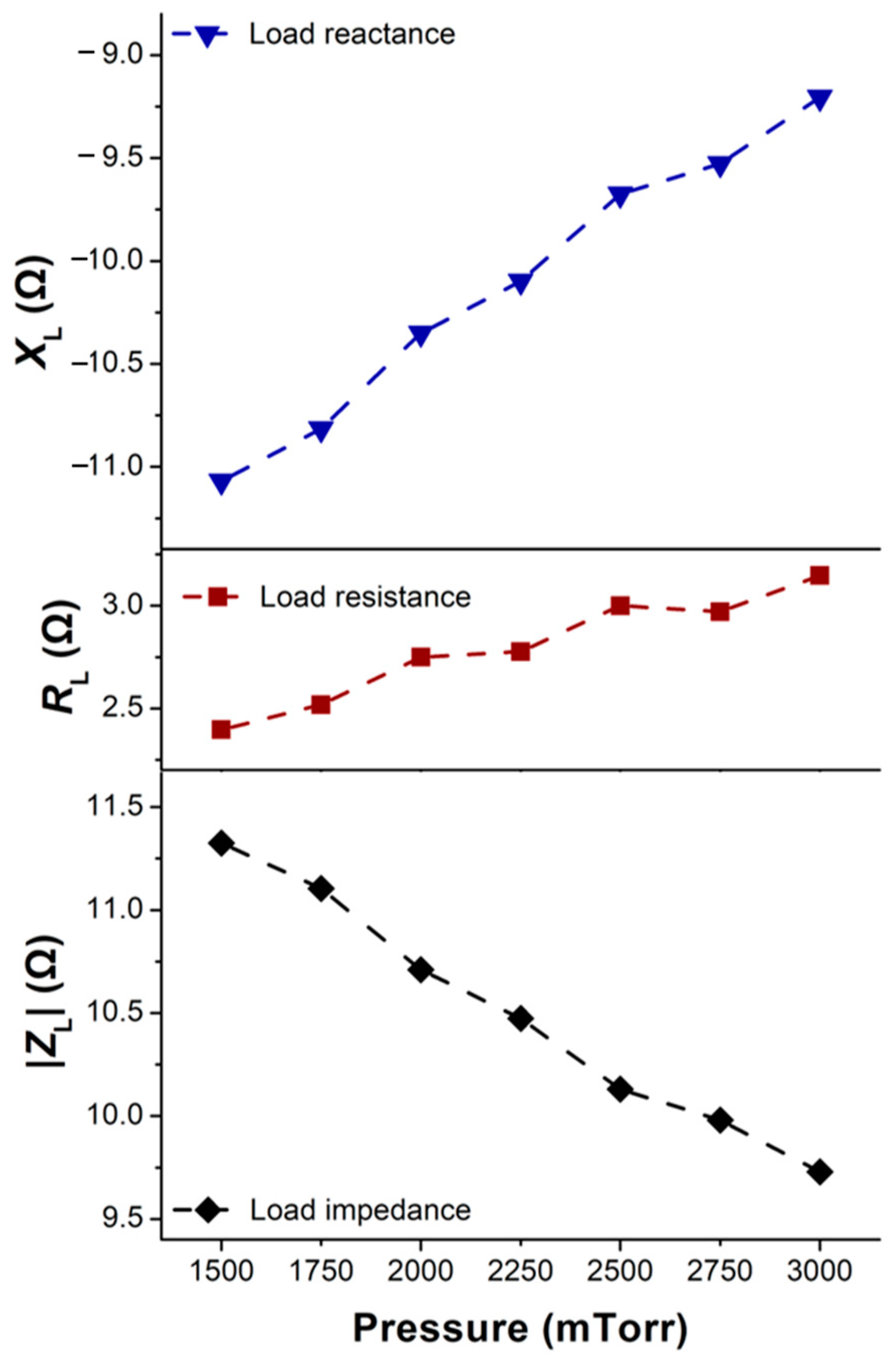
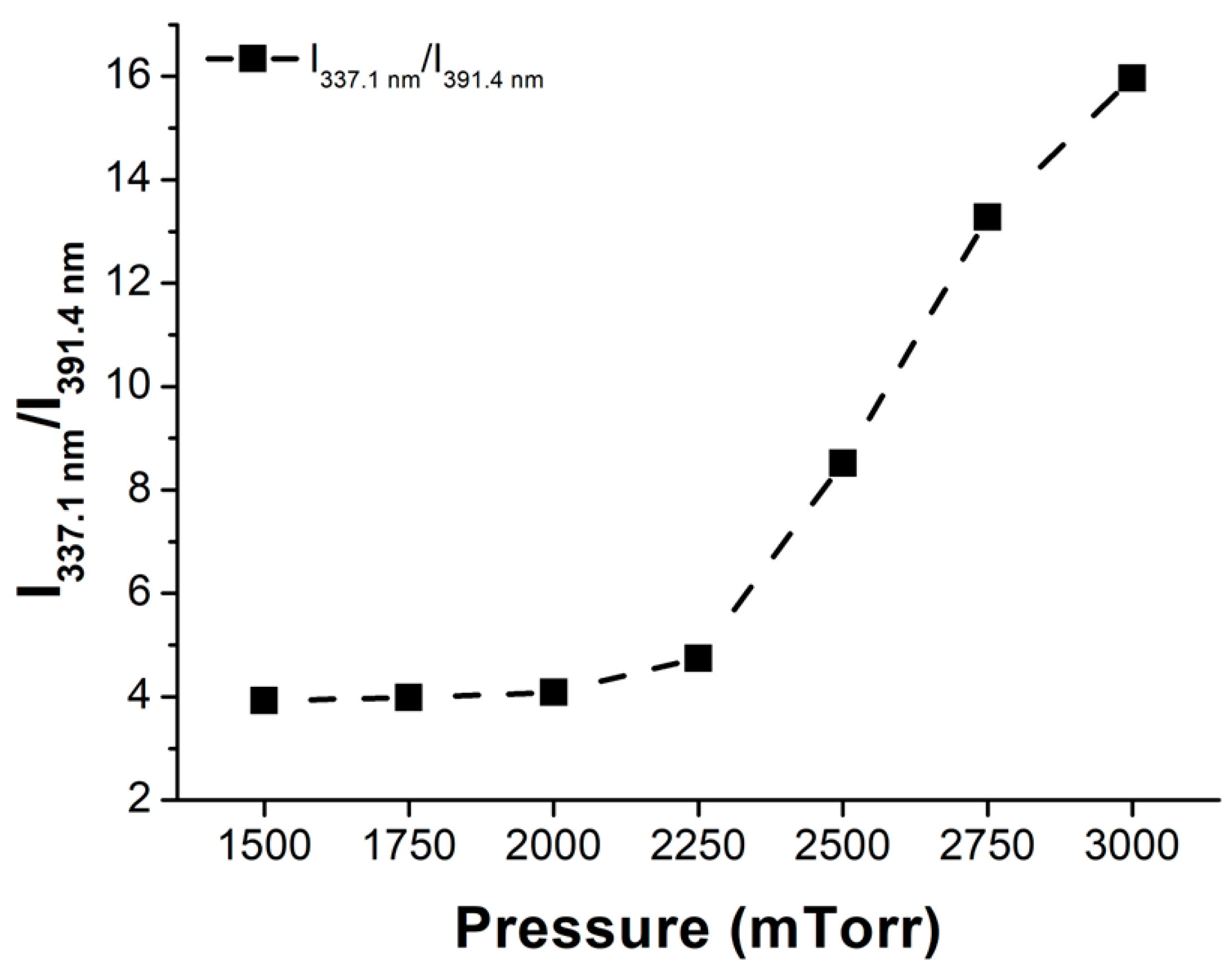
4.2. Result of Pressure Split Test and Discussion
5. Conclusions
Author Contributions
Funding
Data Availability Statement
Conflicts of Interest
References
- Kim, M.H.; Hong, S.J. Equipment Condition Monitoring of Multiple Oxide-Nitride Stack Layer Deposition Process. IEEE Trans. Semi. Manuf. 2023, 36, 645–652. [Google Scholar] [CrossRef]
- Kim, M.H.; Sim, H.E.; Hong, S.J. Part-Level Fault Classification of Mass Flow Controller Drift in Plasma Deposition Equipment. IEEE Trans. Manuf. 2024, 37, 373–380. [Google Scholar] [CrossRef]
- Park, H.K.; Song, W.S.; Hong, S.J. In Situ Plasma Impedance Monitoring of the Oxide Layer PECVD Process. Coatings 2023, 13, 559. [Google Scholar] [CrossRef]
- You, Y.M.; Lee, J.S.; Kim, M.H.; Hong, S.J. Use of plasma process diagnostic sensors for the monitoring of in situ dry cleaning of plasma enhanced chemical vapor deposition chamber. J. Vac. Sci. Technol. B 2024, 42, 042203. [Google Scholar] [CrossRef]
- Kim, J.-Y.; Chung, C.-W. Real-time dielectric-film thickness measurement system for plasma processing chamber wall monitoring. Rev. Sci. Instrum. 2015, 86, 123502. [Google Scholar] [CrossRef]
- Bang, J.-Y.; Yoo, K.; Chung, C.-W. Real-time observation of the capacitance variation in a surface dielectric layer in radio frequency discharge. J. Appl. Phys. 2012, 111, 043305. [Google Scholar] [CrossRef]
- Lee, J.; Kim, K. A Study on the Development of Real-Time Chamber Contamination Diagnosis Sensors. Sensors 2025, 25, 20. [Google Scholar] [CrossRef]
- Kasashima, Y.; Kurita, H.; Kimura, N.; Ando, A.; Uesugi, F. Monitoring of inner wall condition in mass-production plasma etching process using a load impedance monitoring system. Jpn. J. Appl. Phys. 2015, 54, 060301. [Google Scholar] [CrossRef]
- Kasashima, Y.; Uesugi, F. Monitoring method for deposited film causing particles in mass-production plasma etching process using a load impedance monitoring system. In Proceedings of the 2016 International Symposium on Semiconductor Manufacturing (ISSM), Tokyo, Japan, 12–13 December 2016. [Google Scholar] [CrossRef]
- Kasashima, Y.; Tabaru, T.; Ikeda, T. Feasibility Study of Monitoring of Particle Generation in Plasma Etching Process by Plasma Impedance Measurement. J. Semi. Technol. Sci. 2023, 23, 50–55. [Google Scholar] [CrossRef]
- Han, C.; Koo, Y.; Kim, J.; Choi, K.; Hong, S. Wafer Type Ion Energy Monitoring Sensor for Plasma Diagnosis. Sensors 2023, 23, 2410. [Google Scholar] [CrossRef]
- Park, H.; Kim, J.; Cho, S.; Kim, K.; Jang, S.; Choi, Y.; Lee, H. Development of Wafer-Type Plasma Monitoring Sensor with Automated Robot Arm Transfer Capability for Two-Dimensional In Situ Processing Plasma Diagnosis. Sensors 2024, 24, 1786. [Google Scholar] [CrossRef] [PubMed]
- Park, S.-B.; Yeom, H.-J.; Hwang, D.-Y.; Kim, Y.-J.; Lee, H.-C.; Kim, J.H. Measurement of Electron Density in High-pressure Plasma Using a Microwave Cutoff Probe. J. Appl. Phys. 2024, 136, 243301. [Google Scholar] [CrossRef]
- Kim, J.-H.; Yoon, M.-Y.; Kim, G.; Kwon, H.-C.; Kim, J.-H.; Choe, H.-H. Numerical Investigation of Plasma Properties in Ar/SiH4 Inductively Coupled Plasmas Considering Electron Energy Distribution Functions. J. Appl. Phys. 2024, 136, 093303. [Google Scholar] [CrossRef]
- You, K.H.; You, S.J.; Kim, D.W.; Na, B.K.; Seo, B.H.; Kim, J.H.; Shin, Y.H.; Seong, D.J.; Chang, H.Y. A Cutoff Probe for the Measurement of High Density Plasma. Thin Solid Films 2013, 547, 250–255. [Google Scholar] [CrossRef]
- Neumann, G.; Bänziger, U.; Kammeyer, M.; Lange, M. Plasma-density Measurements by Microwave Interferometry and Langmuir Probes in an RF Discharge. Rev. Sci. Instrum. 1993, 64, 19–25. [Google Scholar] [CrossRef]
- Li, B.; Li, H.; Wang, H.; Xie, J.; Liu, W. Theoretical and Experimental Study of the Microwave Cut-off Probe for Electron Density Measurements in Low-temperature Plasma. J. Appl. Phys. 2011, 110, 073308. [Google Scholar] [CrossRef]
- An, S.; Hong, S.J. Spectroscopic Analysis of NF3 Plasma with Oxygen Additive for PECVD Chamber Cleaning. Coatings 2023, 13, 91. [Google Scholar] [CrossRef]
- An, S.; Choi, J.E.; Kang, J.E.; Lee, J.; Hong, S.J. Eco-Friendly Dry-Cleaning and Diagnostics of Silicon Dioxide Deposition Chamber. IEEE Trans. Semi. Manufac. 2024, 37, 207–221. [Google Scholar] [CrossRef]
- Kim, K.E.; Kang, J.E.; Hong, S.J. In Situ Monitoring of Plasma Ignition Step During Photoresist Stripping Using O2/N2 and O2/Ar. J. Korean Phys. Soc. 2023, 82, 173–180. [Google Scholar] [CrossRef]
- Jang, H.; Nam, J.; Kim, C.-K.; Chae, H. Real-Time Endpoint Detection of Small Exposed Area SiO2 Films in Plasma Etching Using Plasma Impedance Monitoring with Modified Principal Component Analysis. Plasma Process Polym. 2013, 10, 850–856. [Google Scholar] [CrossRef]
- Kanoh, M.; Yamage, M.; Takada, H. End-point Detection of Reactive Ion Etching by Plasma Impedance Monitoring. Jpn. J. Appl. Phys. 2001, 40, 1457. [Google Scholar] [CrossRef]
- Jang, D.B.; Hong, S.J. In-Situ Monitoring of Multiple Oxide/Nitride Dielectric Stack PECVD Deposition Process. Trans. Electr. Electron. Mater. 2018, 19, 21–26. [Google Scholar] [CrossRef]
- Yamazawa, Y. Electrode Impedance Effect in Dual-frequency Capacitively Coupled Plasma. Plasma Sources Sci. Technol. 2015, 24, 034015. [Google Scholar] [CrossRef]
- Yamazawa, Y.; Nakaya, M.; Iwata, M.; Shimizu, A. Control of the Harmonics Generation in a Capacitively Coupled Plasma Reactor. Jpn. J. Appl. Phys. 2007, 46, 7453. [Google Scholar] [CrossRef]
- Lafleur, T.; Delattre, P.A.; Booth, J.P.; Johnson, E.V.; Dine, S. Radio Frequency Current-Voltage Probe for Impedance and Power Measurements in Multi-Frequency Unmatched Loads. Rev. Sci. Instrum. 2013, 84, 015001. [Google Scholar] [CrossRef]
- Shin, D.; Hong, S.J. Improved Impedance Matching Speed with Gradient Descent for Advaned RF Plasma System. J. Vac. Sci. Technol. B 2023, 41, 064002. [Google Scholar] [CrossRef]
- Min, J.; Chae, B.; Suh, Y.; Kim, J.; Kim, H. Next-Generation Variable Capacitors to Reduce Capacitance Variable Time Using SiC MOSFETs and p-i-n Diodes in 13.56-MHz RF Plasma Systems. IEEE J. Emerg. Sel. Top. Power Electron. 2022, 10, 1353–1362. [Google Scholar] [CrossRef]
- Lee, J.; Hong, S. Dual-Frequency RF Impedance Matching Circuits for Semiconductor Plasma Etch Equipment. Electronics 2021, 10, 2074. [Google Scholar] [CrossRef]
- Zhang, C.; Ordóñez, R. Impedance Matching in Semiconductor Plasma Processing Chamber. In Extremum-Seeking Control and Applications: A Numerical Optimization-Based Approach; Zhang, C., Ordóñez, R., Eds.; Springer: Berlin/Heidelberg, Germany, 2012; pp. 133–153. [Google Scholar] [CrossRef]
- Yu, S.; Wang, Y.; Chen, Z.; Wang, Z.; Wang, L.; Jiang, W.; Schulze, J.; Zhang, Y. Impedance matching assistance based on frequency modulation for capacitively coupled plasmas. J. Appl. Phys. 2025, 137, 033301. [Google Scholar] [CrossRef]
- Min, J.; Suh, Y. Auto-Bias Electrical Variable Capacitor of Reduced Active Component Count and Voltage Stress for 13.56 MHz RF Plasma Process. IEEE Trans. Ind. Appl. 2022, 58, 4994–5004. [Google Scholar] [CrossRef]
- Liebermann, M.A.; Lichtenberg, A.J. Principles of Plasma Discharges and Materials Processing, 2nd ed.; John Wiley & Sons: Hoboken, NJ, USA, 2005; pp. 387–460. [Google Scholar]
- Mansuroglu, D. Capacitively Coupled Radio Frequency Nitrogen Plasma Generated at Two Different Exciting frequencies of 13.56 MHz and 40 MHz analyzed using Langmuir probe along with optical emission spectroscopy. AIP Adv. 2019, 9, 055205. [Google Scholar] [CrossRef]
- Long, M. Power Efficiency Oriented Optimal Design of High Density CCP and ICP Sources for Semiconductor RF Plasma Processing Equipment. IEEE Trans. Plasma Sci. 2006, 34, 443–454. [Google Scholar] [CrossRef]
- Park, J.-H.; Cho, J.-H.; Yoon, J.-S.; Song, J.-H. Machine Learning Prediction of Electron Density and Temperature from Optical Emission Spectroscopy in Nitrogen Plasma. Coatings 2021, 11, 1221. [Google Scholar] [CrossRef]
- Qayyum, A.; Zeb, S.; Ali, S.; Waheed, A.; Zakaullah, M. Optical Emission Spectroscopy of Abnormal Glow Region in Nitrogen Plasma. Plasma Chem. Plasma Process. 2005, 25, 551–564. [Google Scholar] [CrossRef]
- Paris, P.; Aints, M.; Valk, F.; Plank, T.; Haljaste, A.; Kozlov, K.; Wagner, H.-E. Reply to comments on ‘Intensity ratio of spectral bands of nitrogen as a measure of electric field strength in plasmas. J. Phys. D Appl. Phys. 2005, 38, 3894. [Google Scholar] [CrossRef]
- Mutsukura, N.; Kobayashi, K.; Machi, Y. Plasma Sheath Thickness in Radio-frequency Discharges. J. Appl. Phys. 1990, 68, 2657–2660. [Google Scholar] [CrossRef]
- Mostafaoui, M.; Benyoucef, D. Electrical Model Parameters Identification of Radiofrequency Discharge in Argon Through 1D3V/PIC-MC Model. Plasma Sci. Technol. 2018, 20, 095401. [Google Scholar] [CrossRef]
- Bose, A.; Narakathu, B.; Bazuin, B.; Atashbar, M. Modelling and Simulation of Microplasma Discharge Device for Sterilization Applications. Proceedings 2018, 2, 948. [Google Scholar] [CrossRef]
- You, K.H.; You, S.J.; Kim, D.W.; Na, B.K.; Seo, B.H.; Kim, J.H.; Chang, H.Y. Measurement and Analysis of Electron-neutral Collision Frequency in the Calibrated Cutoff Probe. Phys. Plasmas 2016, 23, 033509. [Google Scholar] [CrossRef]


| Acronyms | Meaning |
|---|---|
| Total impedance | |
| Total resistance | |
| Total reactance | |
| Load impedance | |
| Load resistance | |
| Load reactance | |
| Series impedance | |
| Series reactance | |
| Shunt impedance | |
| Shunt reactance | |
| Electron-neutral collision frequency | |
| Electron mass | |
| Electron density | |
| Plasma electron frequency | |
| Permittivity of vacuum | |
| Area of sheath (Area of electrode) | |
| Sheath thickness | |
| Ionic mean free path | |
| Intrinsic capacitance of the plasma | |
| Sheath capacitance | |
| Bulk plasma resistance | |
| Bulk plasma inductance |
| Component | Value |
|---|---|
| L1 | 200 nH |
| L2 | 1.05 μH |
| VC1 | 35–500 pF |
| VC2 | 35–1000 pF |
| N2 (sccm) | RF Power (W) | Pressure (mTorr) | Electrode Gap (mm) |
|---|---|---|---|
| 3000 | 200−500 (Increments by 50) | 2250 | 16 |
| 350 | 1500−3000 (increments by 250) |
Disclaimer/Publisher’s Note: The statements, opinions and data contained in all publications are solely those of the individual author(s) and contributor(s) and not of MDPI and/or the editor(s). MDPI and/or the editor(s) disclaim responsibility for any injury to people or property resulting from any ideas, methods, instructions or products referred to in the content. |
© 2025 by the authors. Licensee MDPI, Basel, Switzerland. This article is an open access article distributed under the terms and conditions of the Creative Commons Attribution (CC BY) license (https://creativecommons.org/licenses/by/4.0/).
Share and Cite
Kim, H.G.; Lee, J.; Hong, S.J. Impedance Monitoring of Capacitively Coupled Plasma Based on the Vacuum Variable Capacitor Positions of Impedance Matching Unit. Electronics 2025, 14, 2022. https://doi.org/10.3390/electronics14102022
Kim HG, Lee J, Hong SJ. Impedance Monitoring of Capacitively Coupled Plasma Based on the Vacuum Variable Capacitor Positions of Impedance Matching Unit. Electronics. 2025; 14(10):2022. https://doi.org/10.3390/electronics14102022
Chicago/Turabian StyleKim, Hwang Gyu, Jiseok Lee, and Sang Jeen Hong. 2025. "Impedance Monitoring of Capacitively Coupled Plasma Based on the Vacuum Variable Capacitor Positions of Impedance Matching Unit" Electronics 14, no. 10: 2022. https://doi.org/10.3390/electronics14102022
APA StyleKim, H. G., Lee, J., & Hong, S. J. (2025). Impedance Monitoring of Capacitively Coupled Plasma Based on the Vacuum Variable Capacitor Positions of Impedance Matching Unit. Electronics, 14(10), 2022. https://doi.org/10.3390/electronics14102022