Review

Multi-Source Energy Harvesting Systems Integrated in Silicon: A Comprehensive Review

by
Vasiliki Gogolou
1,2,*,
Thomas Noulis
2,3 and
Vasilis F. Pavlidis
1
1
Department of Electrical and Computer Engineering, Aristotle University of Thessaloniki, 54124 Thessaloniki, Greece
2
Center for Interdisciplinary Research and Innovation (CIRI-AUTH), 57001 Thessaloniki, Greece
3
Electronics Laboratory, Department of Physics, Aristotle University of Thessaloniki, 54124 Thessaloniki, Greece
*
Author to whom correspondence should be addressed.
Electronics 2025, 14(10), 1951; https://doi.org/10.3390/electronics14101951
Submission received: 12 April 2025 / Revised: 7 May 2025 / Accepted: 9 May 2025 / Published: 11 May 2025

Abstract

The integration of multi-source energy harvesting (EH) systems into silicon presents a promising avenue for powering autonomous, low-power devices, particularly in applications such as the Internet of Things (IoT), biomedical implants, and wireless sensor networks, where power efficiency and small-size solutions are crucial. This review provides a detailed technical assessment of energy harvesting schemes—including photovoltaic, mechanical, thermoelectric, and radio frequency energy harvesting—and the integration of their associated electronic circuits into silicon integrated solutions. The EH systems are critically analyzed based on their architectures, the number and type of input sources, and key performance metrics such as energy conversion efficiency, output power delivered to loads, silicon area footprint, and degree of integration (e.g., reliance on external components). By examining current advancements and practical implementations, crucial design parameters are assessed for state-of-the-art integrated silicon energy harvesting systems. Furthermore, based on current trends, future research directions are outlined to enhance EH efficiency, reliability, and scalability, paving the way for fully integrated silicon-based EH systems for the next-generation self-powered electronic devices.

1. Introduction

The growing demand for energy-efficient, miniaturized, and autonomous systems drives the need for innovative power solutions [1]. As the proliferation of devices, such as IoT sensors, wearable electronics, and wireless sensor networks continues to expand, the limitations of traditional batteries—such as their limited lifespan and the need for frequent replacements—become more apparent. Thus, powering devices without traditional methods is increasingly important in modern applications. While there are various approaches to achieving this, including wireless power transfer (WPT), which actively transmits energy from a power source to a device over short distances [2,3,4], energy harvesting technologies have emerged as a promising alternative, capable of converting ambient energy from the surrounding environment into usable electrical power [5]. EH captures and converts ambient energy from the environment—such as light, motion, or heat—into electrical energy to power low-energy devices for small, remote, or low-power applications (Figure 1). This shift towards energy harvesting is critical for achieving truly autonomous systems that can operate without reliance on batteries or external power sources, paving the way for sustained functionality in diverse applications.
Energy harvesting systems encompass a variety of technologies designed to capture energy from different environmental sources, including thermal (heat), piezoelectric (vibration), photovoltaic (light), and RF sources [6,7]. Each of these technologies offers unique advantages depending on the environment and application, but individually, they often suffer from intermittency and limited energy output. By harnessing multiple energy sources concurrently, multi-source energy harvesting systems aim to overcome these limitations, offering enhanced reliability, higher energy conversion efficiency, and continuous power availability [8]. Today’s energy conversion systems are increasingly advancing toward silicon-based integration. Silicon power devices, which have dominated power electronics for decades, form the backbone of current power conversion technologies and are essential for renewable energy generation. These designs have demonstrated significant advancements in efficiency and performance, driving the widespread adoption of power electronics and establishing themselves as fundamental to global energy infrastructure [9,10,11,12].
These trends, along with the growing need for miniaturization and integration of electronic components into portable and area-restrained applications, underscore the importance of such systems being integrated on chip. A generalized circuit model for multi-input energy harvesting systems is illustrated in Figure 2. In this architecture, each energy source is connected to a dedicated harvester configured to the nature of the source’s output. The harvested energy is then conditioned through appropriate power conversion stages, including alternating current to direct current (AC–DC) and direct current to direct current (DC–DC) converters, to achieve the desired voltage levels. Maximum Power Point Tracking (MPPT) algorithms are often employed to maximize energy extraction efficiency. Finally, power management and control circuits regulate energy flow to the load, ensuring optimal performance and reliable operation.
This review provides a comprehensive technical assessment of energy harvesting schemes—including photovoltaic, mechanical, thermoelectric, biofuels and radio frequency energy harvesting—and their integration into silicon-based electronic systems. Unlike previous reviews, this work uniquely emphasizes both integration and multi-source operation in depth. The EH systems are critically analyzed with respect to the following:
  • System architectures, including the number and type of input energy sources.
  • Key performance metrics, such as energy conversion efficiency, output power delivered to the load, silicon area footprint, and degree of integration (e.g., reliance on external components).
  • Design trade-offs and integration challenges in achieving compact, high-performance EH solutions.
This structured evaluation aims to highlight the current state of the art, identify technological limitations, and outline directions for future development in the field of low-power energy harvesting systems.

2. Energy Harvesting Technologies Trends

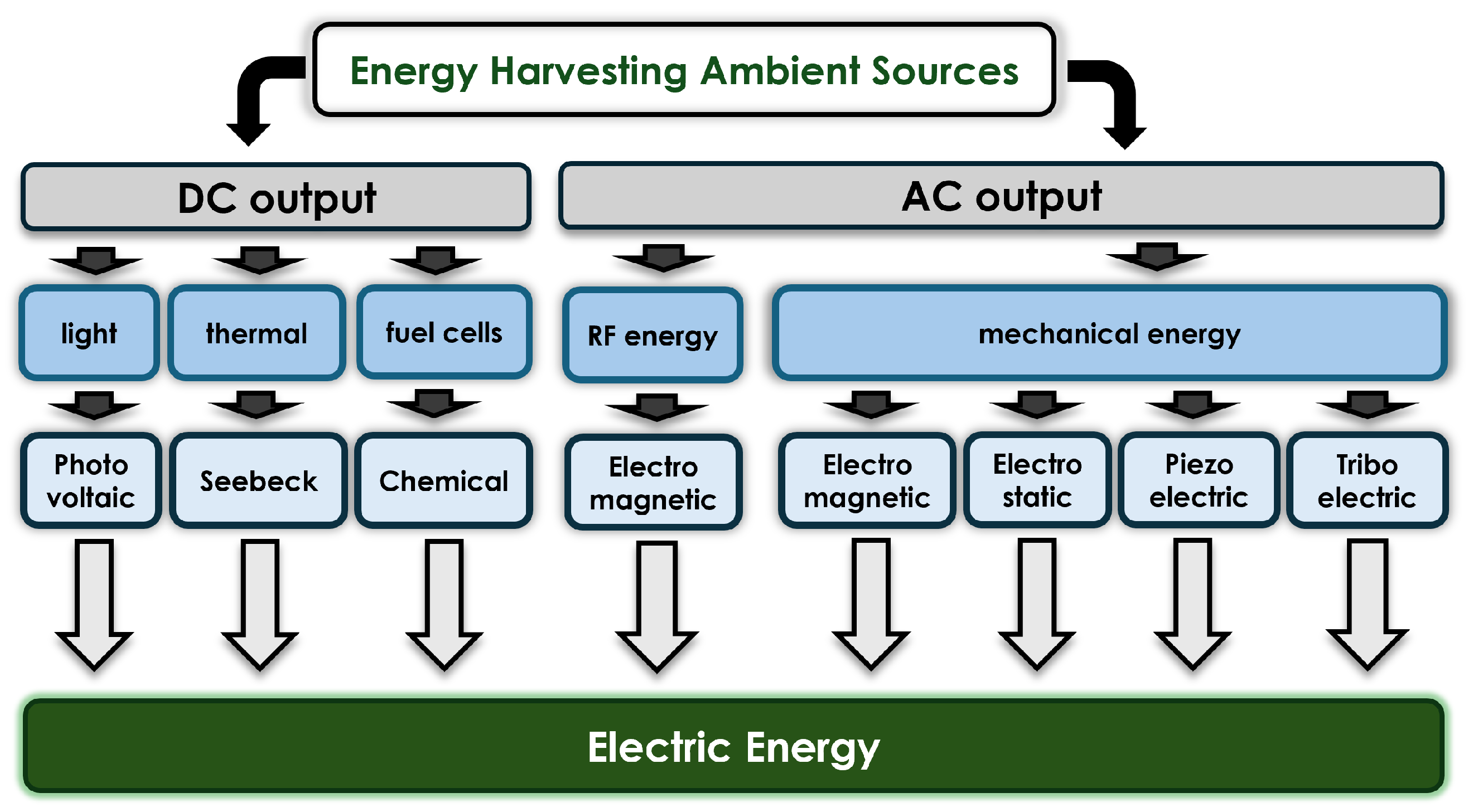
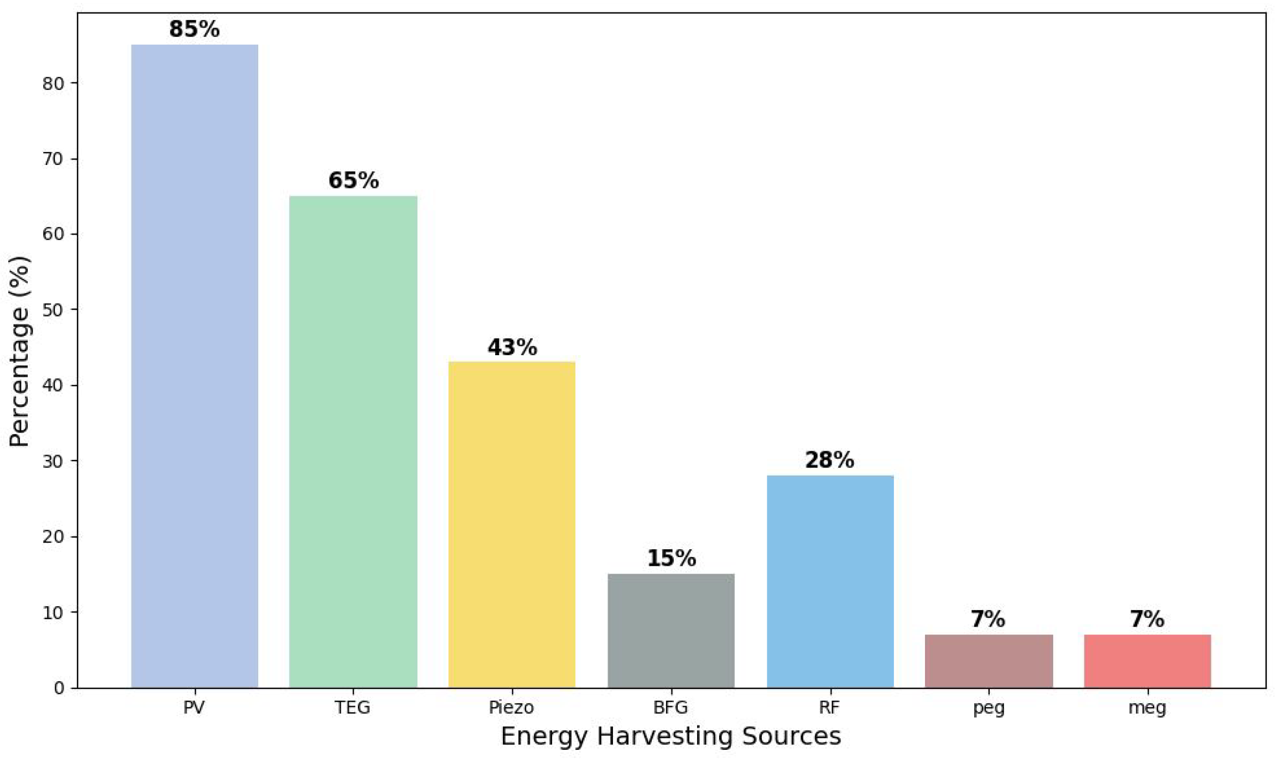
2.1. Ambient Energy Harvesters

In state-of-the-art silicon integrated System-on-Chip (SoC) energy harvesting solutions, a diverse selection of ambient energy sources is exploited, aligned with the evolving advancements in the semiconductor industry. As silicon technology progresses towards higher efficiency, lower power consumption, and greater integration density, the methods and materials of harvesting ambient energy have similarly evolved to exploit these improvements. These energy scavengers are optimized to enhance the functionality of modern silicon designs, paving the way for self-sustaining electronic systems across a wide range of applications. Ambient energy sources can generate either DC or AC outputs, necessitating specialized circuit design to efficiently extract, convert, and store the harvested energy for use in electronic systems (Figure 3). For DC inputs, energy harvesting systems employ DC–DC converter schemes, such as boost, buck, or buck-boost converters, to efficiently adjust the input voltage to the desired output level. In contrast, for AC inputs, the process typically begins with AC-to-DC conversion using rectification circuitry. The rectified signal is subsequently fed into a DC–DC converter to optimize the voltage level for energy storage or direct load connection. The below discussion of current trends in popular ambient energy sources presented in Figure 4 is structured into these two categories: DC types and AC types.

2.1.1. Energy Harvesters with DC Output

Light energy harvesting is one of the oldest and most established renewable energy methods, converting light to electricity through photovoltaic (PV) cells. Silicon photovoltaic cells’ rigid structure and higher weight make them challenging to integrate into compact, lightweight, and portable systems required for IoT applications. Additionally, they generally underperform in ambient light conditions and become cost-inefficient when operating at low energy conversion levels. Hence, the research is focused on solution-processed photovoltaic cells, which offer low-cost fabrication, flexibility, and efficient energy conversion, especially under low-light conditions, such as indoor environments. Unlike traditional silicon PVs, these third-generation cells—comprising dye-sensitized, organic, quantum dot, and perovskite solar cells—present advanced characteristics, such as broad bandgap tunability, lightweight design, and compatibility with flexible substrates. The above attributes make third-generation cells ideal for powering modern low-power IoT devices, including sensors, RFID tags, and Bluetooth beacons [13].
Thermoelectric generators (TEGs) operate based on the Seebeck effect, where a temperature gradient across a thermoelectric material creates a voltage that drives an electric current. Micro-TEGs, quite popular in cutting-edge applications, are compact devices designed to harvest low-grade waste heat and convert it into electrical power, typically in the range of micro- to milliwatts [14]. They are well-suited for powering applications such as wearable electronics, wireless sensors, and medical devices. Commonly fabricated from thermoelectric materials like Bi2Te3 and Sb2Te3, micro-TEGs utilize advanced fabrication techniques, including electroplating, micro-electromechanical systems (MEMS) technology, silicon-based methods, and screen-printing. A key challenge for micro-TEGs is achieving a large temperature difference ( Δ T ) between the hot and cold ends to maximize power output and efficiency. Recent advancements have focused on innovative designs and fabrication methods to address this challenge. For instance, cross-plane micro-TEGs with thick thermocouple pillars, vertical silicon nanowire-based micro-TEGs, and planar TEGs have been developed, showing higher power densities [15]. These advancements are paving the way for more efficient and versatile micro-TEGs in modern applications.
Organic fuel cells, including microbial fuel cells (MFCs) and enzymatic fuel cells, are an innovative type of fuel cell that generates electricity by leveraging biological catalysts rather than metals or synthetic materials. Although still in developmental stages, organic fuel cells hold significant potential for environmental applications, including remote sensors and biodegradable power sources. Current research focuses on enhancing biocatalyst efficiency, increasing power output, and improving the durability of these cells for use in renewable energy systems, environmental monitoring, and low-power electronics [16].

2.1.2. Energy Harvesters with AC Output

Mechanical energy, abundantly present in our environment through sources like human motion, is a promising form of renewable energy. Technologies for harvesting this energy include piezoelectric, triboelectric, electromagnetic, and electrostatic methods. Among these harvesters, piezoelectric technology is preferred due to its higher energy conversion efficiency and adaptability to a range of applications. Piezoelectric materials are classified into natural and synthetic types. Natural materials, such as Rochelle salt, quartz, and bone, were the first identified with piezoelectric properties. Synthetic piezoelectric materials can be further divided into ceramics, polymers, and composites, each offering distinct advantages. Novel fabrication techniques like solution casting, melt spinning, and electrospinning have been developed to support the customization and scaling of these materials, making piezoelectric harvesting a vital solution for the future of renewable energy [17]. Research has also expanded to novel mechanical energy harvesting sources, such as triboelectric energy harvesting. This technique involves the electrification of two distinct insulating materials through electrostatic induction, resulting in one surface acquiring a positive charge and the other a negative charge, thereby generating an electrical potential difference (EPD) between them. Triboelectric nanogenerators (TENGs) offer benefits such as low-cost implementation and adaptability to specific applications, making this energy harvesting method particularly attractive for future developments [18].
Radio frequency energy harvesting (RFEH) is an emerging technology that captures radio frequency signals and converts them into usable electrical energy, allowing low-power devices to function wirelessly. A typical RFEH system comprises an antenna for capturing RF signals, an impedance matching network for efficient power transfer, a rectifier to convert the RF signal from alternating current to direct current, a voltage multiplier to enhance the DC voltage, and energy storage elements like batteries or supercapacitors to retain the harvested energy. As 5G networks expand and the IoT ecosystem grows, RFEH has gained attention for its potential to power billions of connected devices sustainably. Since higher frequencies offer increased received power for a fixed antenna size, RF energy harvesting is particularly promising for millimeter-wave (mmWave) applications. However, challenges such as low power conversion efficiency due to harmonic losses at high frequencies remain present. Future trends in RFEH target optimizing rectenna (i.e., rectifying antenna) designs, developing high-efficiency materials, and integrating RFEH with mmWave 5G networks to support compact, self-sustaining wireless devices in smart cities, healthcare, and industrial applications [19].
Table 1 presents a comprehensive overview of various energy harvesting technologies, highlighting their power output capabilities and real-world application scenarios. By aligning each technology with indicative use cases, informed decision-making in the design and deployment of self-powered or low-power electronic systems can be achieved.
As energy harvesters continue to advance in response to their compactness and performance, offering improved power density and energy extraction efficiency, the electronic systems used for harnessing this energy must also evolve. Given that all components must be battery-powered, small in size and form factor, and sufficiently versatile for integration into portable wearable devices, energy harvesting systems are increasingly miniaturized and integrated into silicon. Discrete implementations become obsolete, and the trend is shifting towards fully integrated solutions. The following sections discuss the progress made so far in silicon-integrated circuits, focusing on the number of ambient energy sources exploited and the architectural choices made to optimize performance.

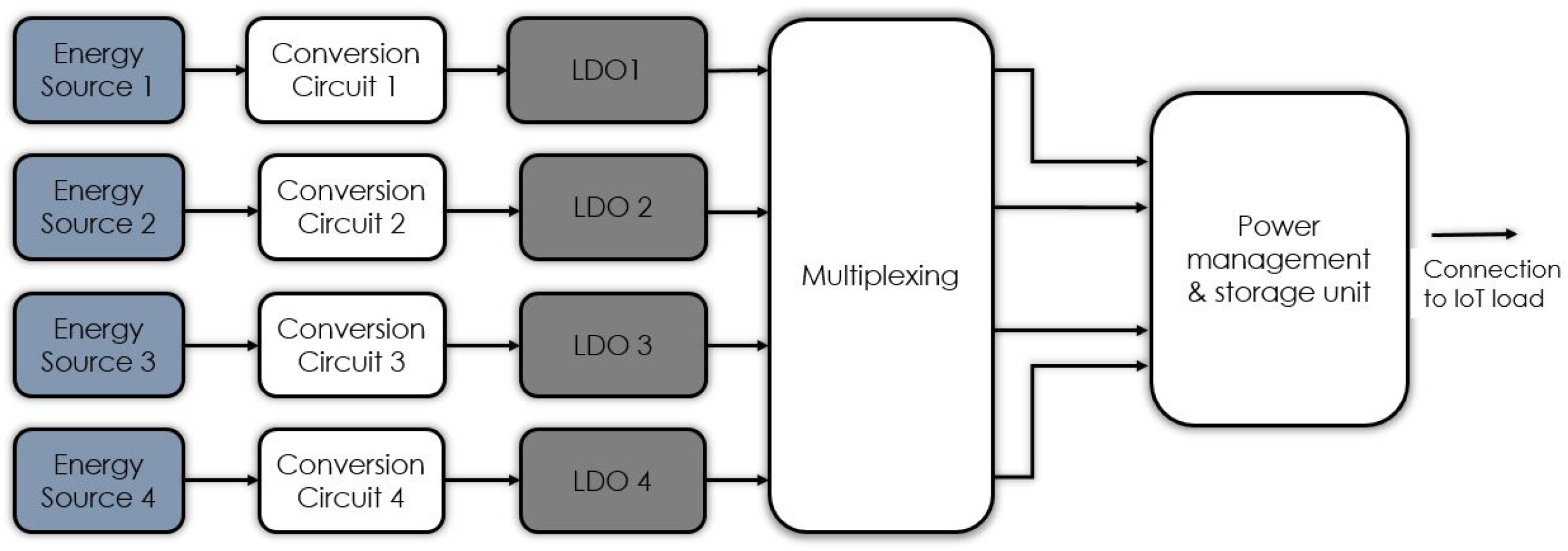
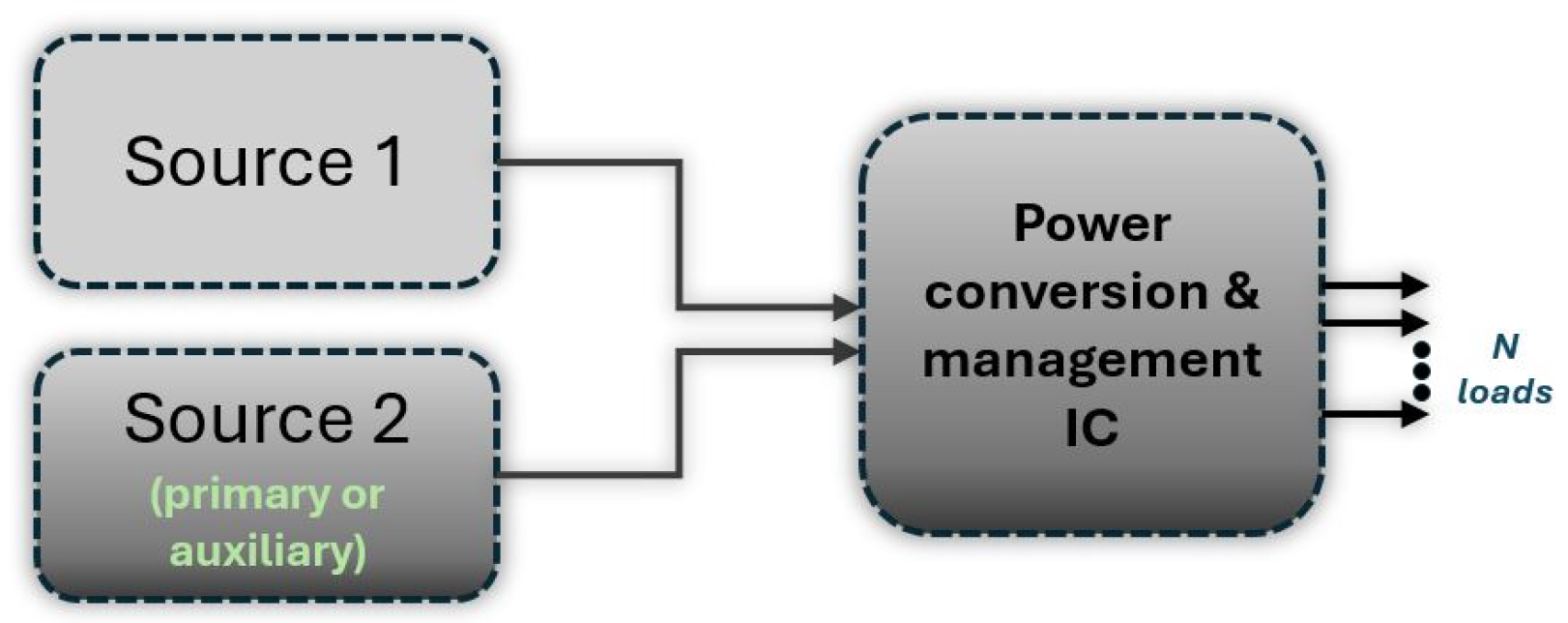
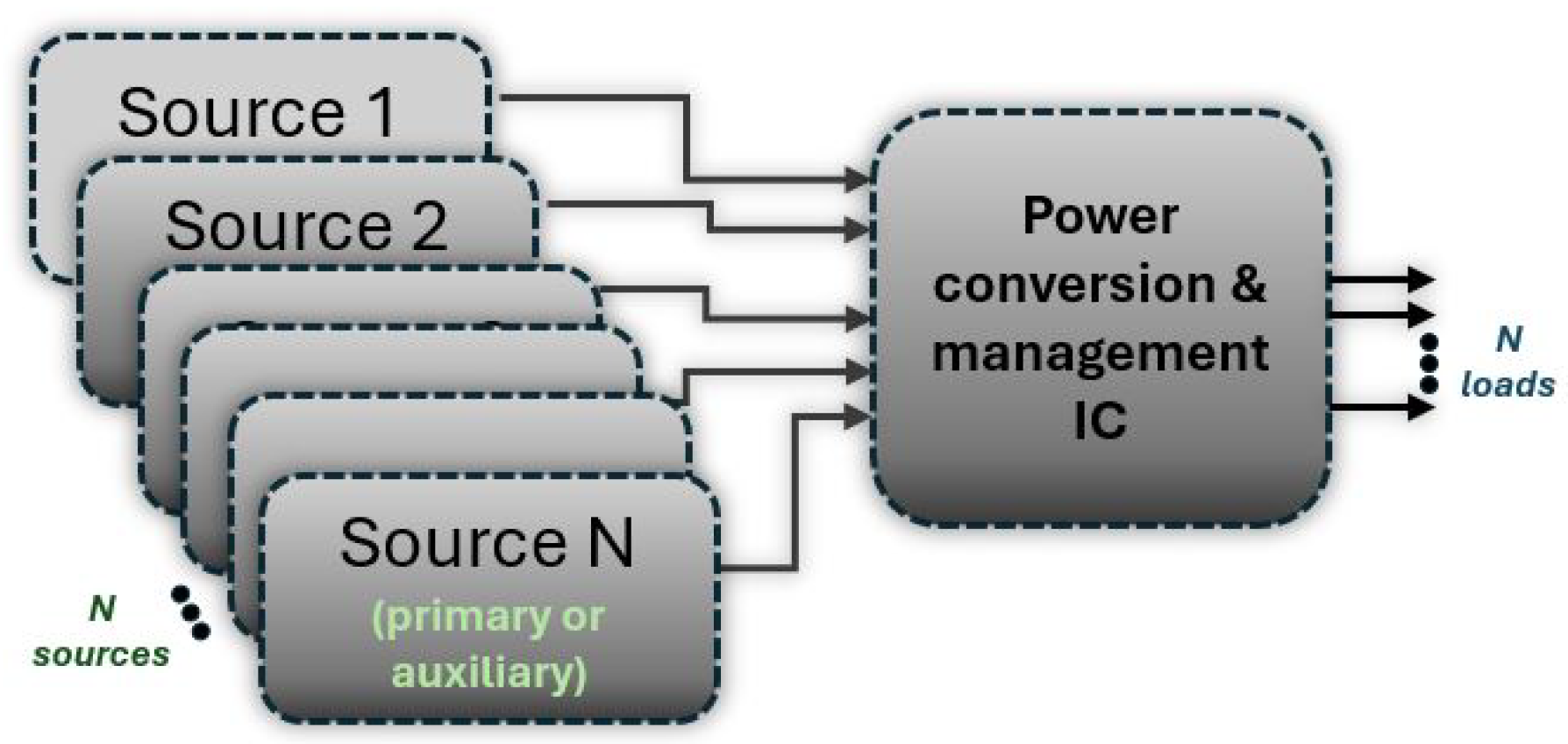
2.2. Main Types of Energy Harvesting System Architectures

In the early stages of energy harvesting development, single-input, single-output (SISO) architectures were the first to be implemented, particularly in discrete, high-power systems as well as in low-power, small-area applications [25,26,27]. These architectures, which typically harvested energy from a single source—such as solar or thermal—to power a single load, were simple and easy to implement but inherently limited by the variability and intermittency of their energy source. As EH technologies evolved across a broad range of applications—from large-scale grid systems to ultra-low-power wearables and IoT devices—single-input, multiple-output (SIMO) configurations emerged [28,29,30]. These allowed a single energy harvester to supply multiple loads or functional subsystems, improving energy distribution and enabling more sophisticated system operation, especially in platforms with multiple sensor or communication modules.
In recent years, multiple-input energy harvesting systems have become more popular because they can collect energy from different sources at the same time, improving reliability and efficiency [31,32]. By using multiple energy sources, these systems provide a stable power supply, even if one source is unavailable.
A variety of architectures have been proposed to enable effective multi-source energy harvesting, each with distinct trade-offs. Complementary energy harvesting relies on a primary harvester for the main energy supply, while secondary sources power auxiliary units (Figure 5) [33]. Although this setup allows parallel operation, it fails to aggregate the harvested energy, leading to suboptimal utilization. Power ORing schemes improve system simplicity by connecting harvesters in parallel through diodes, enabling automatic source selection (Figure 6). However, the associated diode voltage drops reduce overall efficiency, and only the strongest source contributes to the output at any given time [34]. To address these losses, voltage threshold-based switching replaces diodes with active switches, allowing dynamic source selection based on predefined voltage conditions [35]. Yet, these approaches are often sequential in nature, preventing true concurrent harvesting and leaving some input energy untapped. In linear regulator summation architectures, each source is linked to a dedicated low-dropout regulator (LDO), with their outputs merged into a shared storage element (Figure 7) [36]. While this approach allows simultaneous harvesting, it suffers from control complexity and limits on capacitor sizing, which constrain its energy capacity and scalability.
A more space-efficient alternative is the shared-inductor DC-DC converter, where a single inductor is time-shared among multiple sources, as depicted in Figure 8 [37,38]. These architectures allow multiple energy sources to connect to a single inductor, which efficiently switches between sources, collecting power sequentially rather than simultaneously. This shared inductor approach reduces component requirements and circuit complexity and is therefore a popular choice for practical, compact designs.
The next section provides a detailed discussion of state-of-the-art silicon-integrated energy harvesting systems. Although these systems are generally referred to as multi-source, they can be classified into two main categories. The first category includes systems that utilize two input sources (dual input systems), which are quite common. The second category encompasses more advanced attempts that employ multiple input sources to more effectively sustain the operation of the system.

2.3. Overview of State-of-the-Art Multi-Source Energy Harvesting Systems

Based on the above analysis of multi-source energy harvesting schemes, there is a need to design and implement a multi-source energy harvesting architecture that minimizes external components, supports low-power operation, and maximizes the utilization of ambient energy sources. This section examines recent advancements in these systems, focusing on what they currently achieve and how they are paving the way toward an optimal energy harvesting solution for future self-powered devices.
To facilitate straightforward comparisons and clearly outline the advantages of each system, a dedicated figure of merit (FoM) has been established:
FoM = P o u t max × e f f Silicon Area × N x t r n l
where:
  • P o u t max : The maximum output power of the system delivered to the load.
  • eff: Maximum efficiency of the system.
  • Silicon Area: The silicon footprint of the system.
  • N xtrnl : Number of external components used for the system.

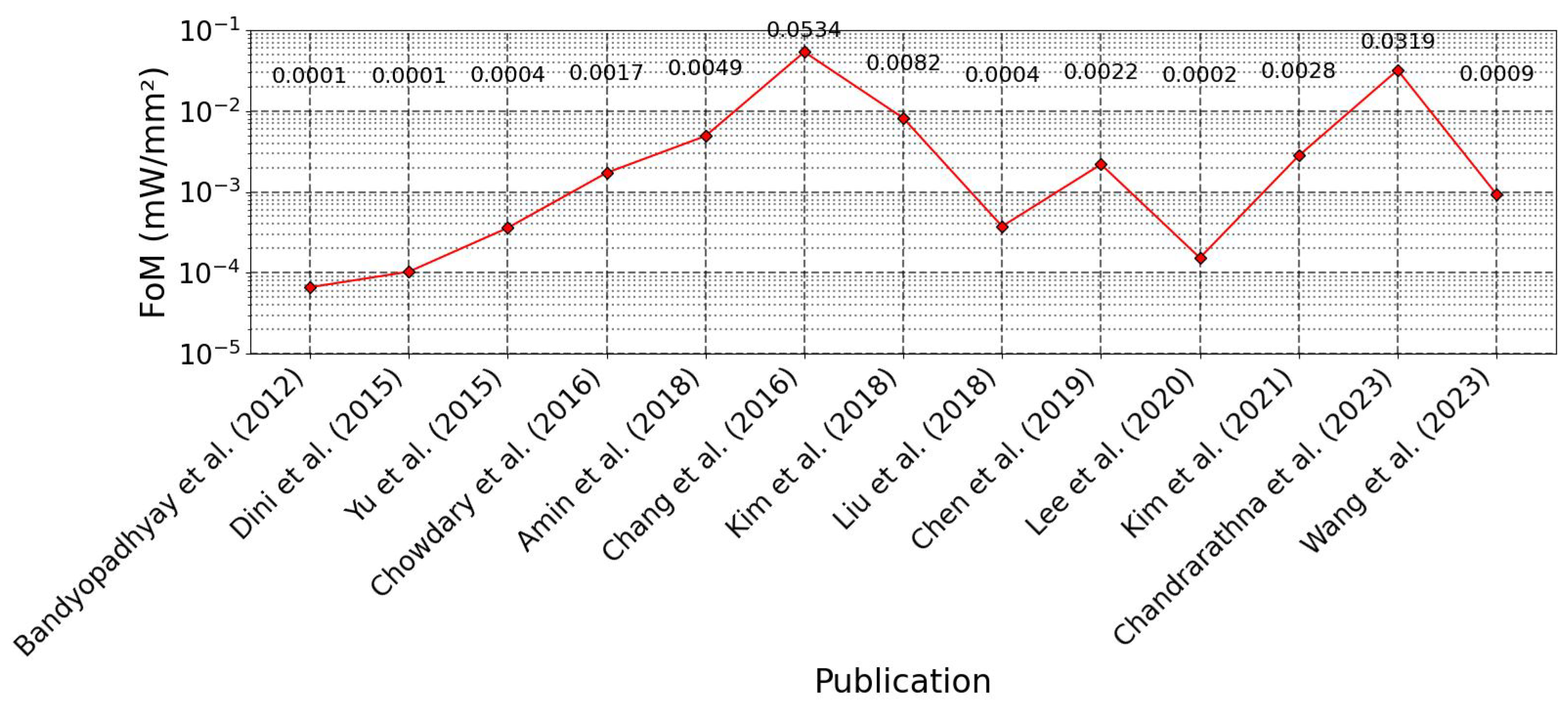
2.3.1. Dual Input Energy Harvesting Systems

The simplest form of multiple-input energy harvesting is the dual-input architecture. In this setup, two input sources provide energy to a single dedicated load (Figure 9). This configuration is widely used due to its straightforward design and reliability, as demonstrated in numerous published works. This approach was among the first used in multi-source energy harvesting and remains widely utilized due to its simplicity and reliability.
Early implementations predominantly utilized PV cells supplemented by battery storage, realized in legacy semiconductor processes exceeding 350 nm. A dual-source energy harvesting interface circuit tailored for low-power biomedical sensing applications can concurrently harvest and convert energy from solar cells and piezoelectric vibration sources, providing a stable and efficient power supply across diverse environmental conditions [39]. The system includes an AC-DC converter, switched-capacitor voltage combiner, and a pulse frequency modulation (PFM) boost switching regulator to manage wide input voltage variations (0.2 V to 1.7 V) and produce a stable DC output (1.8 V to 3.7 V). The presented architecture, while simple and not extensively detailed, represents a first approach to systems that harvest energy from multiple inputs. An optimized EH system for indoor wireless sensor networks (WSNs) builds on the concept of versatility in such systems, demonstrating the capability to operate in multiple states [40]. By introducing a power converter with only three switches and a novel energy-recycling strategy, the system efficiently manages power flows among the PV module, battery, and load through three modes: harvest, backup, and recycle. Switch-size optimization and reduced switch count enhance efficiency, achieving a peak conversion efficiency of 93% and minimizing chip area. The system also supports a wide load voltage range and includes a self-oscillation feature for reliable startup, suitable for low-power, space-constrained WSN applications that operate in indoor lighting. This approach outperforms present solutions in compactness, and adaptability. Lu et al. present a dual-input energy harvesting system designed to efficiently extract and manage power from multiple sources (two at a time) [41]. The architecture utilizes a single inductor to optimize power transfer, offering three outputs: a regulated voltage output, an unregulated voltage output, and a rechargeable battery input. A key innovation is the fast cold-start control method, which accelerates the transition from a low-efficiency state to high-efficiency operation by charging an initial storage capacitor before powering the battery. The system employs a hysteretic control scheme to regulate output voltage and utilizes a backup battery to ensure continuous operation during periods of insufficient ambient energy. The system demonstrates ultra-low quiescent current consumption, making it highly suitable for low-power applications like wearable electronics and wireless sensor networks.
With the advancement of semiconductor technology and the evolvement of energy harvesters, TEGs have emerged as primary energy sources in such systems, now implemented in 180 nm processes. A dual-input energy harvesting system employs several key techniques to efficiently manage power from both a TEG and a glucose biofuel cell (GBFC) [42]. The system achieves maximum power extraction by matching the input resistances to the internal resistances of the TEG and GBFC. The system is designed with a dual-input, dual-output configuration, allowing it to handle two inputs and provide two outputs—one for the load and the other to power the control circuitry. A digital control block is implemented that monitors the harvesting process, utilizing a state machine to manage switching and minimize losses, while voltage monitors and control signals ensure that harvested energy is transferred to the appropriate output based on demand. Additionally, energy accumulation in capacitors smooths power delivery, enabling stable operation by storing energy from inactive harvesters. These techniques collectively enhance the system’s efficiency, flexibility, and reliability by utilizing two inputs while preventing energy waste, as excess energy is stored in capacitors during inactive cycles.
As stated in Section 2.3.2, piezoelectric transducers (PZT) have gained ground in recent years in energy harvesting applications. However, PZT-based energy harvesting systems face challenges in maximizing charge extraction due to large parasitic capacitance and low mechanical strain under weak vibration conditions. To overcome these limitations, a double pile-up resonance technique is introduced, which markedly improves the energy conversion efficiency of the piezoelectric transducer [43]. The double pile-up resonance technique overcomes these challenges by increasing the voltage output from the PZT at its resonance frequency, optimizing the transfer of mechanical energy into electrical energy. This technique involves tuning the circuit to resonate with the natural frequency of the PZT, allowing for more efficient energy conversion and enabling the system to effectively capture and convert mechanical vibrations into electrical power, even in situations with minimal input vibrations. Therefore, energy extraction efficiency, particularly when using only the PZT, is improved. The overall operation is complemented by utilizing the TEG alongside the PZT to ensure sufficient power generation. Thus, in this case, the second ambient source serves as an auxiliary scheme.
An issue that arises with the concurrent utilization of multiple diverse ambient energy sources is the challenge of managing input sources with significantly different internal resistances. Combining an electromagnetic vibration energy generator (EVG) with a thermoelectric energy generator offers an effective solution to this challenge by enabling complementary energy harvesting from multiple ambient sources [44]. Due to the large disparity in the internal resistances, efficient energy harvesting becomes difficult. To solve this problem, a current boost converter (CBC) can be used, which not only handles resistance transformation but also enables source type conversion between the EVG and TEG. A multi-task maximum power point tracking controller is utilized to boost energy extraction from both sources by continuously adjusting the MPPT process and fine-tuning their outputs for optimal performance. To adapt to fluctuating energy source conditions, an input-dependent clock generator (VCG) is introduced. This component tracks changes in source conditions and generates the appropriate clock signal for the MPPT controller. Additionally, a vibration pulse detector (VPD) is used to monitor the random amplitude and frequency variations of the EVG, ensuring efficient energy harvesting even under uncertain and variable conditions.
Regarding newly introduced mechanical-based EH approaches, Park et al. present the first integrated triboelectric-based energy-harvesting circuit with MPPT functionality based on empirical analysis of triboelectric nanogenerators [45]. By enabling efficient voltage regulation and power extraction from TENGs, significant improvements for IoT applications can be offered where battery-free, sustainable power solutions are essential. A high-voltage dual-input buck converter, specifically designed for triboelectric energy harvesting applications, is employed, incorporating an MPPT system optimized for triboelectric nanogenerators. TENGs generate AC output with varying positive and negative peak voltages; consequently, the proposed system separately harvests each half-wave through a dual-output rectifier to improve extraction efficiency. A root-mean-square MPP analysis using the fractional open-circuit voltage method is employed to optimize power harvesting for each half-wave. The converter employs a single inductor to regulate the high voltages from TENGs, and an HV protection circuit is incorporated to prevent transistor breakdown due to high-voltage stress. The system utilizes synchronous pulse-skipping modulation in discontinuous conduction mode to independently control two DC voltages, ensuring each operates at its corresponding maximum power point. This work provides new insights into energy harvesting from triboelectric materials, which are low-cost and show promising potential for future silicon integrated applications. Another approach for TENG energy harvesting enhances power conversion efficiency by integrating two symmetric buck converters for each phase, using a shared inductor to isolate high input voltages [46]. This technique eliminates the need for additional high-voltage protection circuits and extra capacitors at the switching node, thereby simplifying the system. Furthermore, the extra resistors used in the previous solution [45] are removed, moving towards a more fully integrated design. By employing a diode-based high-voltage sampling circuit, the converter efficiently samples and detects peak voltages without the need for external components. This approach improves both the efficiency and compactness of energy harvesting systems compared to earlier designs.
RF energy harvesting is an emerging technology with great potential for advanced applications in the RF/mmWave design field. However, it encounters challenges, such as low power density, impedance mismatches, efficiency compromises when switching between wideband and narrowband operation, and the requirement for sensitive circuits to effectively convert weak ambient signals into usable energy. The work presented in [47] demonstrates the first dual-antenna, multi-input RF harvesting system using full energy extraction (FEE), significantly improving efficiency, dynamic response, and power conversion in environments with varying RF availability. The system utilizes two rectifier topologies—the Dickson rectifier and the cross-coupled rectifier. In particular, a 4-stage Dickson rectifier is employed for improved efficiency in energy extraction. The FEE controller improves the dynamic response of the system by regulating the discharge of small buffer capacitors, allowing the system to adapt quickly to changing RF input power and achieve higher efficiency. The overall system architecture targets minimization of switching losses and maximization of DC-DC conversion efficiency, particularly at low input power levels.
Most recent works focus on the parallel optimization of multiple energy harvesting system characteristics. One such system is a thermoelectric energy harvesting interface that features a reconfigurable DC-DC converter with dual-conversion mode and a time-based instantaneous linear extrapolation (ILE) MPPT method [48]. This EH system targets applications with varying load conditions, aiming to improve efficiency, reduce energy loss, and enhance stability. The dual-conversion mode, based on a five-switch dual-input dual-output topology, allows power from both the thermoelectric generator and the battery to be transferred to the output in a single switching cycle, maintaining stable output voltage even under heavy loads. The time-based ILE MPPT method constantly monitors the maximum power point without disconnecting the TEG, utilizing an integrated MPPT circuit that adjusts the TEG voltage, thereby preventing the energy losses typically associated with conventional MPPT sampling techniques. This setup ensures consistent energy extraction from the TEG, enabling continuous, adaptive power management and optimal energy use from both the TEG and battery, even as load and environmental conditions fluctuate.
A typical challenge in cutting-edge, area-constrained silicon solutions lies in the performance of the energy harvester. For example, miniature thermoelectric generators used in IoT applications produce very low voltages under typical temperature gradients. To make the energy usable for IoT devices, a DC-DC boost converter is usually required to increase the voltage. Traditional cold-start techniques, such as mechanical switches, one-shot cold-start pulses, and ring oscillators, can initiate operation without the need for a battery, but they require a startup voltage of over 35 mV, which exceeds the output of most miniature TEGs. This limitation can be overcome by a thermoelectric energy harvesting system [49] that comprises a piezoelectric generator (PEG) as a low-voltage starter, leveraging the concurrent generation of heat and vibration in environments such as engines and human body movements. This PEG starter converts kinetic energy into an AC signal, which is then transformed into a clock signal to initiate the boost converter. The high output impedance of the PEG allows the generation of a sufficient voltage to drive the switches of the boost converter, achieving ultra-low-voltage startup. Furthermore, maximum power point tracking is used to optimize energy extraction by aligning the input impedance of the converter with that of the TEG, thus improving the overall power efficiency of the system.
Table 2 summarizes the key information from the state-of-the-art dual-input silicon integrated energy harvesting systems. The percentage utilization of various ambient energy sources in dual-input energy harvesting systems is illustrated in Figure 10. As depicted, TEGs and PVs are the most commonly utilized input harvesters due to their favorable balance between power output (typically in the milliwatt range) and utilization cost. Additionally, they are more readily available in the market. In contrast, mechanical sources, such as piezoelectric devices, are less frequently employed due to the higher cost and the difficulty in finding them available off the shelf. Other sources, such as biofuel cells, remain largely experimental and are challenging to implement in many practical applications.
The output power and peak end-to-end efficiency of each system are presented in Figure 11. The performance of each system is designed to meet the specific demands of the loads that it aims to power. For instance, works such as [40,41,48] target higher-demanding loads. This situation is expected for the first two EH systems, as they represent early studies where the loads were more power-hungry, while the third presents a system characterized by high input power, enabled by the efficient utilization of its energy harvesters. Other EH systems can support outputs in the range of microwatts to a few milliwatts, which is typical for modern-day loads. Additionally, system performance is heavily influenced by the choice of the ambient energy source. To provide an overall evaluation of the dual input integrated EH systems, Figure 12 illustrates the FoM values based on Equation (1) introduced in Section 2.3 for dual-input systems over the years, considering not only the output power and efficiency but also the silicon area used and the number of external components.

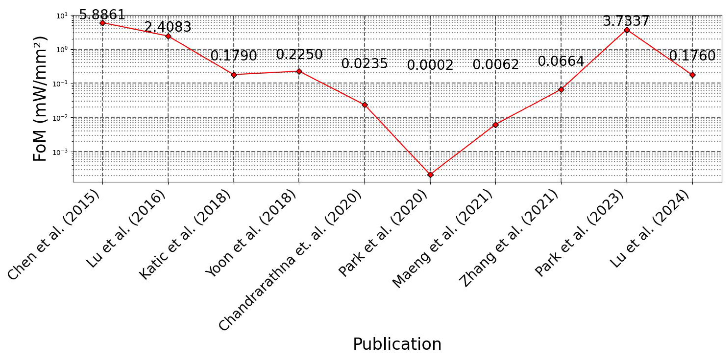
2.3.2. Multi-Input Energy Harvesting Systems

Building on the concept of dual-input systems, the future of energy harvesting is moving towards multi-input configurations, which combine more than two energy sources to maximize energy extraction and ensure the extended survival of the system being powered (Figure 13).
As discussed in Section 2.2, most of these systems utilize a shared inductor to efficiently manage energy from multiple sources. This approach is the most common method for ensuring optimal power conversion while minimizing the component count.
An early multi-input architecture for efficient energy harvesting from solar, thermal, and vibration sources is demonstrated to achieve significant efficiency improvement over traditional two-stage systems [38]. The architecture includes a reconfigurable multi-input, multi-output switch matrix that combines energy from photovoltaic cells, thermoelectric generators, and piezoelectric transducers, accommodating input voltages ranging from 20 mV to 5 V. By using a single inductor, the system efficiently extracts maximum power from each source at the same time. The dual-path design enables the primary converter to directly supply the load when sufficient energy is available, while the auxiliary converter is triggered to draw from stored energy when required. The focus of the research then shifted to reducing the power consumption of the system to improve efficiency and extend its lifetime. An ultra-low power energy harvesting solution is implemented for battery-less systems, extracting energy from multiple heterogeneous sources such as vibrations, light, heat, and electromagnetic radiation [50]. The core innovation lies in the use of a buck-boost converter to combine these energy sources, ensuring that each one, regardless of its output voltage, can charge a shared energy storage component. By implementing an energy-efficient design that significantly cuts static power consumption, the system delivers a major enhancement over current technologies. Additionally, the system features an integrated circuit that minimizes power losses, enabling the harvesting of energy even at very low power levels (down to microwatts). This capability makes it particularly well-suited for applications in wearable electronics and implantable biosystems. A single-inductor dual-input tri-output buck-boost (DITOBB) converter can be used to lower quiescent power [51]. The converter effectively transfers input power from a PV panel to both the load and energy storage in a single conversion step, thereby improving system efficiency. The system operates with a combined pulse-skipping modulation and pulse-frequency modulation to regulate two output voltages, consuming an ultra-low quiescent power. Additionally, the converter optimizes the maximum power point tracking of the PV panel and manages battery charging with surplus energy. To further reduce power consumption, the design utilizes a low-power relaxation oscillator as the system’s clock generator, eliminating the need for reference voltage generators or comparators. The clock frequency is dynamically adjusted in response to output power demands, controlled by a frequency-modulation algorithm. This strategy ensures the circuit operates with high efficiency across a wide range of load conditions while keeping quiescent current consumption to an absolute minimum.
With the advancement of RF/mmWave applications, the harvesting of RF energy is also exploited in multi-source systems. A modular MPPT DC-DC buck-boost converter harvests energy from multiple ambient sources, such as vibrations, indoor light, and RF energy [52]. The system employs a shared inductor and incorporates two innovative techniques for efficient power extraction. First, the frequency of oscillators, responsible for energy harvesting from the different sources, is automatically tuned to match a comparator frequency using a successive approximation algorithm, ensuring MPPT operation. Secondly, the system operates in a discontinuous conduction mode to maintain a steady peak current through the inductor, minimizing losses from resistance and switching during energy transfer while avoiding current reversal. It also features a configurable switched-mode output voltage. Coupled with a low-dropout regulator, it ensures a reliable and stable output for sensitive applications. Another multi-source energy harvesting system efficiently captures both thermal and RF energy [53]. A multi-input boost converter is combined with an RF rectifier, enabling simultaneous harvesting of DC from thermoelectric generators and AC from RF sources. The utilized timing control strategy optimally exploits the idle time of the inductor for energy transfer during both harvesting and regulating modes, enhancing overall energy delivery capability for applications in battery-less devices and IoT technologies.
An advanced power management unit designed for compact, net-zero energy systems, implemented in 28 nm technology—an ultra-low process for such systems—has been proposed in [37]. This unit is capable of aggregating maximum power from three energy sources (light, heat, and biofuels) while regulating three output rails and managing a battery, all using a single inductor (MISIMO). The scheme simplifies the design by time-sharing the inductor and dynamically switching between different configurations based on real-time energy availability and load demand. This mechanism reduces the component count, which is ideal for small-form-factor IoT devices. The single-stage buck-boost converter operating in discontinuous conduction mode improves power management by reducing losses and optimizing both battery charging and power delivery to the load. These capabilities enable adaptation to changing environmental conditions, enhance energy harvesting efficiency in resource-limited settings, and represent a significant advancement in power management for IoT applications.
Many systems focus on maximizing the number of input sources utilized. An event-driven single-inductor energy harvesting power management IC is introduced in [54], designed for IoT edge nodes, capable of harvesting from six different input sources (both DC and AC). The system features a multi-input, single-inductor, multi-output architecture that enables efficient power conversion across various energy sources. The main innovation stems from the use of high-frequency switching and refined control strategies, which allow for smaller inductors and capacitors, quicker transitions between power states, and a more compact, space-efficient design. The circuit also incorporates maximum power point tracking and battery monitoring on a single chip, delivering superior dynamic performance and energy efficiency compared to conventional energy harvesting systems. A single-inductor triple-input–triple-output (SITITO) buck–boost converter designed for energy harvesting from photovoltaic cells and thermoelectric generators has also been proposed [55]. It features two regulated outputs: one for analog circuits and a second one for digital circuits, alongside a storage capacitor for excess energy. The SITITO converter operates in three modes: single-source mode (SSM), dual-source mode (DSM), and backup mode (BM). The innovative cycle-by-cycle source tracking technique ensures that the converter selects the input source based on the maximum power point of the transducers. Additionally, an adaptive on-time circuit equipped with adaptive peak inductor current (APIC) control dynamically tunes the ON-time of the power transistors, enhancing overall conversion efficiency. Overall, the SITITO converter effectively harnesses energy from multiple sources, making it suitable for low-power applications. The proposed system’s converter has the ability to manage multiple operational modes, allowing for flexible input sourcing. Another single-inductor triple-source quad-mode (SITSQM) energy-harvesting interface comprises a reversely polarized energy recycling (RPER) technique that enhances conversion efficiency at low input voltages and extends the output power range [56]. The converter utilizes a buck–boost topology to efficiently harvest energy from photovoltaic cells and a thermoelectric generator, delivering a regulated output while storing excess energy in a reverse-polarity storage capacitor. The system operates in four modes: harvesting mode (HM), recycling mode (RM), storing mode (SM), and backup mode (BM), with automatic mode selection based on input and load conditions, enabling advanced versatility for usage in a wide range of applications.
Power management units (PMUs) that include non-rechargeable supplies have also appeared. For example, a single-inductor dual-input dual-output (SIDIDO) PMU for a hybrid system combines a non-rechargeable battery with photovoltaic energy harvesting [57]. The PMU aims to address the power management challenges in IoT devices, which typically require multiple voltage levels for different components. To improve energy efficiency, the system employs a dual-output DC-DC converter that shares a single inductor, reducing both cost and footprint without compromising performance. A standout feature is the implementation of a two-dimensional adaptive on-time (2-D AOT) control strategy, which effectively minimizes output voltage ripple across a broad input voltage range (0.55–1.4 V) and output range (0.4–0.6 V), overcoming the shortcomings of conventional pulse-frequency modulation techniques. Additionally, the system uses sequential pulse-skip modulation to improve load regulation and medium-to-light load efficiency, along with an automatic mode-selection mechanism to minimize battery usage. The circuit features a high level of integration using low-power CMOS components, including a bandgap reference circuit, to deliver dependable performance tailored for low-power IoT applications.
In [58], the first integrated system dedicated solely to RF energy harvesting is presented, featuring an innovative event-driven multi-input multi-output (EDMIMO) buck-boost converter. This system is designed for efficient RF energy harvesting across a wide power range, optimizing power conversion and regulation for varying ambient RF signal levels. The design incorporates an adaptive maximum power point tracking mechanism that combines a linear search of the fractional open-circuit voltage with a binary search approach for optimizing power switch sizing. This dual-method strategy enhances both MPPT and power conversion efficiency. As a result, the converter achieves over 95% MPPT efficiency and up to 85% power conversion efficiency, even in fluctuating energy harvesting environments. The design effectively considers losses from conduction, switching, and control circuitry, showcasing the potential for powering low-energy devices in diverse environments.
Recent works focus on the parallel usage of multiple sources and the maximization of end-to-end efficiency through advanced techniques. Kim et al. introduce in [59] a multi-input single-inductor multi-output energy-harvesting interface that efficiently extracts power from three independent sources and regulates three different output voltages. The converter uses a novel double-conversion rejection technique that reduces unnecessary double power conversions by up to 81.8% during light-load conditions, significantly improving efficiency. A buck-based dual-conversion mode is also applied to enhance power conversion efficiency and increase the maximum output power. To achieve this, the system includes an adaptive controller that adjusts the peak inductor current to manage the charging period, along with a digitally controlled detector that identifies the optimal point where current reaches zero, depending on the operating mode. The proposed converter achieves an impressive peak end-to-end efficiency of 90.2% and a maximum output power of 24 mW, offering a 7.52% efficiency improvement and a 1.85-times increase in power compared to conventional buck-boost converters. These advancements provide a more efficient solution for energy harvesting, particularly for wireless sensor networks and IoT applications.
A power management unit tailored for hybrid energy harvesting is proposed in [60], achieving exceptional performance with high tracking efficiency and end-to-end efficiency. Key features include a streamlined architecture that utilizes a single inductor for efficient energy collection, a backup power controller for recycling surplus energy, and an innovative boost–buck conversion mode for simultaneous tracking of multiple energy sources. The power management unit integrates an active bias-flip rectifier for handling alternating current inputs, along with three boost converters for low-voltage sources and a buck converter for high-voltage regulation. It adjusts its operation across four modes depending on the load, enhancing overall energy harvesting efficiency and ensuring effective power distribution. To further improve performance, it uses advanced methods like adaptive impedance tuning and a perturb-and-observe strategy to extract maximum energy from available sources.
Multi-source energy harvesters are often limited by conventional time-division multiplexing (TDM) schemes that struggle in continuous current mode (CCM). A single-inductor hybrid energy synchronous extraction circuit overcomes this issue by featuring a synchronous electric charge extraction system for alternating current energy and two buck-boost converters for direct current energy [61]. This combination allows operation in either TDM mode for separate energy harvesting from different sources or in serial stack resonance mode for simultaneous energy extraction from multiple sources. The system is equipped with a photovoltaic cell, a thermoelectric generator, and two flexible piezoelectric transducers, leveraging adaptability to various application requirements.
Table 3 summarizes the salient features of the presented multi-source energy harvesting systems. As illustrated in Figure 14, in silicon integrated multi-source energy harvesting systems, thermoelectric generators and photovoltaic cells remain the most commonly utilized input sources. The output power and peak efficiency (Figure 15) highlight the importance of these systems, as they target comparable output power ranges, making them suitable for similar applications, particularly in the IoT domain. The FoM graph (Figure 16) demonstrates a consistent trend for improvement in power density per unit area over the years, reflecting the ongoing efforts to optimize these systems for maximum energy extraction within a compact silicon footprint. The works in [55,56,57] present a slight reduction in the FoM, primarily due to the reliance on a higher number of external components. Notably, MISIMO [37] continues to set the benchmark for integrated energy harvesting systems, offering a gold standard in the field.
Considering the results of this section, together with the previous section, it is obvious that metrics such as efficiency, output power, silicon area, input voltage range, and usage of external components are interdependent. Efficiency and output power are fundamentally limited by power conversion losses, which are a combination of switching and conduction losses, and control overhead. Higher efficiency implementations demand more advanced power conversion topologies (e.g., utilization of MPPT, multi-phase converters), which increase control complexity and the required silicon area. The selected process node also affects performance through transistor speed and leakage currents. In general, the selection of smaller nodes offers better integration density and faster switching but can introduce higher static leakage and reduced breakdown voltages, limiting the input range and robustness of the EH system. A wider Vin range requires adaptive regulation control (e.g., dual-path or reconfigurable converters), which increases circuit complexity and may demand additional passive elements or switches, contributing to a larger footprint and increased dependence on external components. On the other hand, reducing external components enhances monolithic integration and reliability but forces designers to implement on-chip passive elements, which tend to be less efficient. Backup batteries are essential for powering load during source outages; however, they require charge management circuitry that should interface seamlessly with the main harvesting system. This advances the complexity of the control loops, consuming both power and area. Thus, optimizing a multisource energy harvester involves a tightly coupled co-design of architecture, circuit techniques, and process technology to navigate these trade-offs and meet the constraints of IoT, biomedical, or autonomous systems.

2.3.3. Challenges and Strategies for State-of-the-Art Multi-Source Energy Harvesting Systems

Although silicon integration of energy harvesting systems is a core research focus, the analysis of existing works—particularly those exploiting the shared inductor architecture, which remains the most used approach for multi-source energy harvesting—reveals several challenges that are yet to be solved. These include unreliable startup behavior when none of the sources are always present, poor compatibility with low-frequency or pulsed stochastic energy inputs, and complex control requirements due to the coupling of multiple energy paths through a single inductor. Specifically, cold-start becomes problematic when available input power is below the startup threshold, especially if none of the sources are dominant or if energy arrives at random times. Existing cold-start circuits are often designed for a single input type and do not perform well under mixed or low-power conditions. Additionally, pulsed sources, such as RF or mechanical-based harvesters, usually require the system to store energy until a usable threshold is reached. This demands ultra-low leakage storage elements and sub-uW control logic. Also, if this threshold is never reached, the already-collected energy is not used. Shared inductors also introduce regulation and interference issues between power paths, necessitating complex source arbitration, isolation schemes, and smart adaptable control strategies. This comes in disagreement with the need for low power control strategies. Converter designs are also constrained, as the inductor value must be shared across converters optimized for different source characteristics, leading to potential suboptimal efficiency for some sources. Considering all this, future solutions must focus on more adjustable and highly versatile cold-start circuits that can operate from any available source, ultra-low power control architectures that can dynamically prioritize and switch between inputs, exploitation of sleep/power up modes, and reconfigurable converter topologies that preserve isolation and efficiency despite shared passives. Hybrid approaches that combine shared and dedicated inductors possibly offer a promising direction. In addition, efficient energy buffering and cross-source coupling logic will be essential to enable reliable, autonomous operation in real-world environments.

2.3.4. Advancing Toward True Simultaneous Energy Harvesting

Multi-source energy harvesting using a shared inductor partially addresses the stochastic and unpredictable nature of ambient energy sources. However, this approach has two significant limitations: when multiple sources are simultaneously capable of providing energy, the shared inductor restricts concurrent utilization, leading to waste of energy. In addition, although all input sources exploit the same inductor, this element still corresponds to a bulky external component, restricting full silicon integration. To overcome these issues, some initial efforts have been proposed that allow for simultaneous energy extraction from multiple sources, maximizing energy utilization efficiency and enabling full integration on silicon (Figure 17).
Such an attempt introduces an integrated modular multi-source energy harvesting system utilizing the Dickson charge pump scheme and incorporates a hill-climbing algorithm for maximum power point tracking [62]. The system collects power simultaneously from multiple energy sources and boosts their DC voltages to a regulated output. The architecture allows for independent optimization of each charge pump for different sources, ensuring effective energy harvesting and output regulation.
A fully integrated energy harvesting system that simultaneously captures thermal and RF energy for powering low-power wireless sensor networks has also been presented [63]. The system can exploit both DC and AC type ambient sources by combining a charge pump for boosting thermal voltage with a rectification circuit for RF energy conversion. By optimizing key parameters, such as charge pump boosting stages, operating switching frequency, and matching network capacitors, the system provides promising results.
Table 4 summarizes the characteristics of these works. Although these works are early attempts of fully integrated energy harvesting systems with simultaneous harnessing capability, significant challenges lie ahead compared to the inductor-based solutions. Also, for utilization of multiple sources or very low input voltage levels, these schemes require large capacitances for the charge pump core, which leads to an increased silicon footprint and, therefore, a high product-to-cost ratio. In terms of efficiency, charge pumps are less efficient than inductor-based systems, especially at higher conversion ratios and increased load, due to losses that occur in the switching transistors, parasitic capacitances, and the resistance of capacitors. Scalability is another challenge for charge pump designs. They are best suited for small-scale, low-power applications with modest voltage conversion requirements. Their compact size, low cost, and ease of full integration make them ideal for miniaturized systems. However, when a significant voltage step-up is required—necessitating many charge pump stages—the efficiency drops. This limits their applicability in higher power or high-conversion-ratio scenarios. Inductor-based converters, on the other hand, offer better scalability, with efficiency maintained across a broader range of power levels. Although inductors increase in size with power demand, this trade-off is generally more manageable than the stage-dependent limitations of charge pumps. In practical terms, charge pumps are widely used in ultra-low-power systems such as microcontrollers, sensors, RFID tags, and IoT devices, where power demands are minimal and space is constrained. However, for applications requiring high output current, large voltage conversion ratios, or the integration of multiple input sources, charge pumps may require large on-chip capacitors to maintain performance. This increases silicon area and impacts cost-effectiveness. Despite these challenges, this approach represents a promising avenue for the future of multi-source energy harvesting, focusing on the elimination of external components and true concurrent exploitation of multiple environmental sources.

3. Discussion and Future Directions

While silicon integration offers substantial advantages for compact, efficient, and scalable multi-source energy harvesting systems—such as reduced parasitic losses, improved reliability, tighter coupling of control, and power stages—it is not without significant trade-offs. In addition to these system-level considerations, practical integration brings both manufacturing and physical constraints. One of the primary issues is material compatibility: many energy transducers (e.g., piezoelectric, thermoelectric, and photovoltaic materials) are not inherently CMOS-compatible due to thermal budget, contamination risks, or process sequence limitations. This often necessitates heterogeneous integration techniques, each of which introduces alignment, interconnect density, and yield challenges. Thermal considerations are also crucial. Thermal isolation is essential in systems harvesting from temperature gradients (e.g., thermoelectric harvesters), but standard CMOS provides high thermal conductivity paths, reducing the available ΔT across the transducer. Furthermore, substrate coupling, where switching noise or thermal gradients in the substrate affect sensitive analog front-ends, can degrade voltage reference stability, MPPT circuits, and low-noise amplifiers used in the sensing circuits of the system. This calls for careful layout design, guard rings, and the use of deep N-well or silicon-on-insulator processes, which further increase the product-to-cost ratio. From the cost perspective, advanced CMOS nodes often lack high-voltage (HV) options, requiring additional masks for the realization of energy harvesting systems. Costs increase significantly with each added option layer (e.g., HV transistors, thick top metals) and can be prohibitive for low-volume or pure research development. Overall, while fully integrated EH systems offer advanced performance, they require the enablement of a complex design space that includes process limitations, thermal management, analog integrity, and cost scalability. A successful system architecture must therefore be co-optimized across device, circuit, and packaging domains, balancing theoretical performance with practical manufacturability and lifecycle cost.
As a promising future direction, the integration of Wide Bandgap (WBG) and Ultra-Wide Bandgap (UWBG) semiconductor materials—such as silicon carbide (SiC), gallium nitride (GaN), and gallium oxide ( Ga 2 O 3 )—could address many of these limitations. These materials enable higher voltage, frequency, and temperature operation with minimal power loss, paving the way for more compact, energy-efficient, and robust EH systems capable of meeting increasing demands for power density and system miniaturization.

4. Conclusions

The concept of multi-source energy harvesting has been thoroughly reviewed, with a critical assessment of diverse architectures proposed in the literature based on key performance parameters. As illustrated in Figure 18, the publication trends in silicon-integrated systems, particularly in dual-input and truly multi-input configurations, show a consistent increase in the number of papers published, reflecting the growing demand for area-constrained, silicon-integrated solutions. The distribution of process technologies within these categories reveals significant variability, with the 180 nm CMOS standard process emerging as the most commonly used due to its favorable balance of voltage and current ratings and cost-effective tape-out options, making it ideal for energy harvesting applications.
Regarding the exploited input harvesters, thermoelectric generators and photovoltaic cells continue to be the most widely adopted sources due to their favorable balance between power output, cost, and availability. However, other sources, such as piezoelectric, triboelectric, and fuel-based systems, have gained attention over the years, expanding the range of potential energy harvesting solutions. Advanced architectures for voltage and power conversion continue to emerge, pushing the boundaries of these systems towards greater efficiency and flexibility, enabling them to operate in disparate environments and applications.
The trend of improvements in FoM over the years underscores the ongoing focus on optimizing power density within compact designs, which is a challenging task, as several core trade-offs define the design space of state-of-the-art EH platforms. High efficiency requires complex regulation that increases silicon area, while reducing external components often compromises passive performance and control simplicity. Process node selection also plays a critical role—advanced nodes offer better integration but can limit voltage range and increase leakage, complicating deployment in real-world conditions. Shared-inductor multi-source architectures remain common but face unresolved challenges, such as unreliable cold start, poor adaptability to pulsed sources, and cross-path interference. These issues call for more versatile startup circuits, reconfigurable converters, and ultra-low-power control capable of handling diverse input behaviors. Looking ahead, future solutions must emphasize adaptability and autonomy. Hybrid architectures, improved energy buffering, and the integration of wide bandgap materials like GaN or SiC offer promising pathways toward efficient, robust, and fully integrated energy harvesting platforms.

Author Contributions

Conceptualization, V.G., T.N. and V.F.P.; formal analysis, V.G.; investigation, V.G.; data curation, V.G.; writing—original draft preparation, V.G.; writing—review and editing, T.N. and V.F.P.; visualization, V.G. All authors have read and agreed to the published version of the manuscript.

Funding

This research received no external funding.

Conflicts of Interest

The authors declare no conflicts of interest.

References

  1. Qaim, W.B.; Ometov, A.; Molinaro, A.; Lener, I.; Campolo, C.; Lohan, E.S.; Nurmi, J. Towards energy efficiency in the internet of wearable things: A systematic review. IEEE Access 2020, 8, 175412–175435. [Google Scholar] [CrossRef]
  2. Niu, S.; Zhang, C.; Shi, Y.; Niu, S.; Jian, L. Foreign object detection considering misalignment effect for wireless EV charging system. ISA Trans. 2022, 130, 655–666. [Google Scholar] [CrossRef] [PubMed]
  3. Niu, S.; Zhao, Q.; Chen, H.; Niu, S.; Jian, L. Noncooperative Metal Object Detection Using Pole-to-Pole EM Distribution Characteristics for Wireless EV Charger Employing DD Coils. IEEE Trans. Ind. Electron. 2024, 71, 6335–6344. [Google Scholar] [CrossRef]
  4. Niu, S.; Niu, S.; Zhang, C.; Jian, L. Blind-Zone-Free Metal Object Detection for Wireless EV Chargers Employing DD Coils by Passive Electromagnetic Sensing. IEEE Trans. Ind. Electron. 2023, 70, 965–974. [Google Scholar] [CrossRef]
  5. Sun, Y.; Li, Y.Z.; Yuan, M. Requirements, challenges, and novel ideas for wearables on power supply and energy harvesting. Nano Energy 2023, 115, 108715. [Google Scholar] [CrossRef]
  6. Mitcheson, P.D.; Yeatman, E.M.; Rao, G.K.; Holmes, A.S.; Green, T.C. Energy Harvesting from Human and Machine Motion for Wireless Electronic Devices. Proc. IEEE 2008, 96, 1457–1486. [Google Scholar] [CrossRef]
  7. Sanislav, T.; Mois, G.D.; Zeadally, S.; Folea, S.C. Energy Harvesting Techniques for Internet of Things (IoT). IEEE Access 2021, 9, 39530–39549. [Google Scholar] [CrossRef]
  8. Liu, H.; Fu, H.; Sun, L.; Lee, C.; Yeatman, E.M. Hybrid energy harvesting technology: From materials, structural design, system integration to applications. Renew. Sustain. Energy Rev. 2020, 137, 110473. [Google Scholar] [CrossRef]
  9. International Roadmap for Devices and Systems (IRDS™) 2023 Update: More Moore. Available online: https://irds.ieee.org/images/files/pdf/2023/2023IRDS_MM.pdf (accessed on 26 February 2025).
  10. Mandourarakis, I.; Gogolou, V.; Koutroulis, E.; Siskos, S. Integrated Maximum Power Point Tracking System for Photovoltaic Energy Harvesting Applications. IEEE Trans. Power Electron. 2022, 37, 9865–9875. [Google Scholar] [CrossRef]
  11. Gogolou, V.; Karipidis, S.; Noulis, T.; Siskos, S. A frequency boosting technique for cold-start charge pump units. Integration 2024, 94, 102076. [Google Scholar] [CrossRef]
  12. Gogolou, V.; Voulkidou, A.; Karipidis, S.; Noulis, T.; Siskos, S. Design of crosstalk aware energy harvesting system-on-chip. AEU-Int. J. Electron. Commun. 2023, 170, 154850. [Google Scholar] [CrossRef]
  13. Li, B.; Hou, B.; Amaratunga, G.A.J. Indoor photovoltaics, The Next Big Trend in solution-processed solar cells. InfoMat 2021, 3, 445–459. [Google Scholar] [CrossRef]
  14. Jaziri, N.; Boughamoura, A.; Müller, J.; Mezghani, B.; Tounsi, F.; Ismail, M. A comprehensive review of Thermoelectric Generators: Technologies and common applications. Energy Rep. 2020, 6, 264–287. [Google Scholar] [CrossRef]
  15. Liu, S.; Hu, B.; Liu, D.; Li, F.; Li, J.F.; Li, B.; Li, L.; Lin, Y.H.; Nan, C.W. Micro-thermoelectric generators based on through glass pillars with high output voltage enabled by large temperature difference. Appl. Energy 2018, 225, 600–610. [Google Scholar] [CrossRef]
  16. Talkhooncheh, A.H.; Yu, Y.; Agarwal, A.; Kuo, W.W.T.; Chen, K.C.; Wang, M.; Hoskuldsdottir, G.; Gao, W.; Emami, A. A biofuel-cell-based energy harvester with 86% peak efficiency and 0.25-V minimum input voltage using source-adaptive MPPT. IEEE J.-Solid-State Circuits 2021, 56, 715–728. [Google Scholar] [CrossRef]
  17. Bairagi, S.; Shahid-ul-Islam; Shahadat, M.; Mulvihill, D.M.; Ali, W. Mechanical energy harvesting and self-powered electronic applications of textile-based piezoelectric nanogenerators: A systematic review. Nano Energy 2023, 111, 108414. [Google Scholar] [CrossRef]
  18. Walden, R.; Kumar, C.; Mulvihill, D.M.; Pillai, S.C. Opportunities and Challenges in Triboelectric Nanogenerator (TENG) based Sustainable Energy Generation Technologies: A Mini-Review. Chem. Eng. J. Adv. 2022, 9, 100237. [Google Scholar] [CrossRef]
  19. Ramalingam, L.; Mariappan, S.; Parameswaran, P.; Rajendran, J.; Nitesh, R.S.; Kumar, N.; Nathan, A.; Yarman, B.S. The Advancement of Radio Frequency Energy Harvesters (RFEHs) as a Revolutionary Approach for Solving Energy Crisis in Wireless Communication Devices: A Review. IEEE Access 2021, 9, 106107–106139. [Google Scholar] [CrossRef]
  20. Xie, L.; Song, W.; Ge, J.; Tang, B.; Zhang, X.; Wu, T.; Ge, Z. Recent progress of organic photovoltaics for indoor energy harvesting. Nano Energy 2021, 82, 105770. [Google Scholar] [CrossRef]
  21. Yan, J.; Liao, X.; Yan, D.; Chen, Y. Review of Micro Thermoelectric Generator. J. Microelectromechanical Syst. 2018, 27, 1–18. [Google Scholar] [CrossRef]
  22. Slate, A.J.; Whitehead, K.A.; Brownson, D.A.C.; Banks, C.E. Microbial fuel cells: An overview of current technology. Renew. Sustain. Energy Rev. 2019, 101, 60–81. [Google Scholar] [CrossRef]
  23. Song, J.; Gao, L.; Tao, X.; Li, L. Ultra-Flexible and Large-Area Textile-Based Triboelectric Nanogenerators with a Sandpaper-Induced Surface Microstructure. Materials 2018, 11, 2120. [Google Scholar] [CrossRef] [PubMed]
  24. De Mil, P.; Jooris, B.; Tytgat, L.; Catteeuw, R.; Moerman, I.; Demeester, P.; Kamerman, A. Design and Implementation of a Generic Energy-Harvesting Framework Applied to the Evaluation of a Large-Scale Electronic Shelf-Labeling Wireless Sensor Network. EURASIP J. Wirel. Commun. Netw. 2010, 2010, 343690. [Google Scholar] [CrossRef]
  25. Cabello, D.; Ferro, E.; Pereira-Rial, Ó; Martínez-Vázquez, B.; Brea, V.M.; Carrillo, J.M.; López, P. On-Chip Solar Energy Harvester and PMU with Cold Start-Up and Regulated Output Voltage for Biomedical Applications. IEEE Trans. Circuits Syst. I Regul. Pap. 2020, 67, 1103–1114. [Google Scholar] [CrossRef]
  26. Rozgić, D.; Marković, D. A Miniaturized 0.78-mW/cm2 Autonomous Thermoelectric Energy-Harvesting Platform for Biomedical Sensors. IEEE Trans. Biomed. Circuits Syst. 2017, 11, 773–783. [Google Scholar] [CrossRef]
  27. Kwon, D.; Rincón-Mora, G.A. A Single-Inductor 0.35 µm CMOS Energy-Investing Piezoelectric Harvester. IEEE J.-Solid-State Circuits 2014, 49, 2277–2291. [Google Scholar] [CrossRef]
  28. Katic, J.; Rodriguez, S.; Rusu, A. A Dual-Output Thermoelectric Energy Harvesting Interface with 86.6% Peak Efficiency at 30 uW and Total Control Power of 160 nW. IEEE J.-Solid-State Circuits 2016, 51, 1928–1937. [Google Scholar] [CrossRef]
  29. Ozaki, T.; Hirose, T.; Asano, H.; Kuroki, N.; Numa, M. Fully-Integrated High-Conversion-Ratio Dual-Output Voltage Boost Converter with MPPT for Low-Voltage Energy Harvesting. IEEE J.-Solid-State Circuits 2016, 51, 2398–2407. [Google Scholar] [CrossRef]
  30. Abdelmagid, B.A.; Hmada, M.H.K.; Mohieldin, A.N. An Adaptive Fully Integrated Dual-Output Energy Harvesting System with MPPT and Storage Capability. IEEE Trans. Circuits Syst. Regul. Pap. 2023, 70, 593–606. [Google Scholar] [CrossRef]
  31. Song, S.; Wang, D.; Li, M.; Cao, S.; Zheng, F.; Huang, K.; Tan, Z.; Du, S.; Zhao, M. Low-Power On-Chip Energy Harvesting: From Interface Circuits Perspective. IEEE Open J. Circuits Syst. 2024, 5, 267–290. [Google Scholar] [CrossRef]
  32. Gomathy, S.; Senthilnathan, N.; Swathi, S.; Poorviga, R.; Dinakaran, P. Review on multi-input multi output dc-dc converter. Int. J. Sci. Technol. Res. 2020, 9, 428–440. [Google Scholar]
  33. Maghami, I.; Victor, V.A.; Morsy, M.M.; Lach, J.C.; Goodall, J.L. Exploring the complementary relationship between solar and hydro energy harvesting for self-powered water monitoring in low-light conditions. Environ. Model. Softw. 2021, 140, 105032. [Google Scholar] [CrossRef]
  34. Tan, Y.K.; Panda, S.K. Energy Harvesting From Hybrid Indoor Ambient Light and Thermal Energy Sources for Enhanced Performance of Wireless Sensor Nodes. IEEE Trans. Ind. Electron. 2011, 58, 4424–4435. [Google Scholar] [CrossRef]
  35. Kang, T.; Kim, S.; Hyoung, C.; Kang, S.; Park, K. An Energy Combiner for a Multi-Input Energy-Harvesting System. IEEE Trans. Circuits Syst. II Express Briefs 2015, 62, 911–915. [Google Scholar] [CrossRef]
  36. Colomer-Farrarons, J.; Miribel-Catala, P.; Saiz-Vela, A.; Samitier, J. A Multiharvested Self-Powered System in a Low-Voltage Low-Power Technology. IEEE Trans. Ind. Electron. 2011, 58, 4250–4263. [Google Scholar] [CrossRef]
  37. Amin, S.S.; Mercier, P.P. MISIMO: A multi-input single-inductor multi-output energy harvesting platform in 28-nm fdsoi for powering net-zero-energy systems. IEEE J. Solid-State Circuits 2018, 53, 3407–3419. [Google Scholar] [CrossRef]
  38. Bandyopadhyay, S.; Chandrakasan, A.P. Platform Architecture for Solar, Thermal, and Vibration Energy Combining with MPPT and Single Inductor. IEEE J. Solid-State Circuits 2012, 47, 2199–2215. [Google Scholar] [CrossRef]
  39. Chou, Y.Y.; Wu, C.C.; Chen, Y.H.; Huang, Y.C.; Chiu, Y.C.; Tsai, L.J.; Hsieh, W.C.; Li, W.C.; Huang, Y.J.; Lu, S.S. Multi-input energy harvesting interface for low-power biomedical sensing system. In Proceedings of the 2014 International Symposium on Next-Generation Electronics (ISNE), Kwei-Shan Tao-Yuan, Taiwan, 7–10 May 2014; pp. 2–3. [Google Scholar] [CrossRef]
  40. Chen, H.J.; Wang, Y.H.; Huang, P.C.; Kuo, T.H. An energy-recycling three-switch single-inductor dual-input buck/boost DC-DC converter with 93% peak conversion efficiency and 0.5 mm2 active area for light energy harvesting. Dig. Tech. Pap.-IEEE Int. Solid-State Circuits Conf. 2015, 58, 374–375. [Google Scholar] [CrossRef]
  41. Lu, Y.; Yao, S.; Shao, B.; Brokaw, P. A 200 nA single-inductor dual-input-triple-output (DITO) converter with two-stage charging and process-limit cold-start voltage for photovoltaic and thermoelectric energy harvesting. Dig. Tech. Pap.-IEEE Int. Solid-State Circuits Conf. 2016, 59, 368–369. [Google Scholar] [CrossRef]
  42. Katic, J.; Rodriguez, S.; Rusu, A. A high-efficiency energy harvesting interface for implanted biofuel cell and thermal harvesters. IEEE Trans. Power Electron. 2018, 33, 4125–4134. [Google Scholar] [CrossRef]
  43. Yoon, K.S.; Hong, S.W.; Cho, G.H. Double Pile-Up Resonance Energy Harvesting Circuit for Piezoelectric and Thermoelectric Materials. IEEE J. Solid-State Circuits 2018, 53, 1049–1060. [Google Scholar] [CrossRef]
  44. Chandrarathna, S.C.; Lee, J.W. A 580 nW Dual-Input Energy Harvester IC Using Multi-Task MPPT and a Current Boost Converter for Heterogeneous Source Combining. IEEE Trans. Circuits Syst. I Regul. Pap. 2020, 67, 5650–5663. [Google Scholar] [CrossRef]
  45. Park, I.; Maeng, J.; Shim, M.; Jeong, J.; Kim, C. A High-Voltage Dual-Input Buck Converter Achieving 52.9% Maximum End-to-End Efficiency for Triboelectric Energy-Harvesting Applications. IEEE J. Solid-State Circuits 2020, 55, 1324–1336. [Google Scholar] [CrossRef]
  46. Maeng, J.; Park, I.; Shim, M.; Jeong, J.; Kim, C. A High-Voltage Dual-Input Buck Converter with Bidirectional Inductor Current for Triboelectric Energy-Harvesting Applications. IEEE J. Solid-State Circuits 2021, 56, 541–553. [Google Scholar] [CrossRef]
  47. Zhang, Z.; Zhan, C.; Law, M.K.; Jiang, Y.; Mak, P.I.; Martins, R.P. A High-Efficiency Dual-Antenna RF Energy Harvesting System Using Full-Energy Extraction with Improved Input Power Response. IEEE Open J. Circuits Syst. 2021, 2, 436–444. [Google Scholar] [CrossRef]
  48. Park, I.; Jeon, J.; Kim, H.; Park, T.; Jeong, J.; Kim, C. A Thermoelectric Energy-Harvesting Interface with Dual-Conversion Reconfigurable DC-DC Converter and Instantaneous Linear Extrapolation MPPT Method. IEEE J. Solid-State Circuits 2023, 58, 1706–1718. [Google Scholar] [CrossRef]
  49. Lu, T.; Wang, R.; Tang, Z.; Zou, Y.; Yue, X.; Liang, Y.; Gong, H.; Liu, S.; Chen, Z.; Liu, X.; et al. A Thermoelectric Energy Harvesting System Assisted by a Piezoelectric Transducer Achieving 10-MV Cold-Startup and 82.7% Peak Efficiency. IEEE Trans. Power Electron. 2024, 39, 6352–6363. [Google Scholar] [CrossRef]
  50. Dini, M.; Romani, A.; Filippi, M.; Bottarel, V.; Ricotti, G.; Tartagni, M. A nanocurrent power management IC for multiple heterogeneous energy harvesting sources. IEEE Trans. Power Electron. 2015, 30, 5665–5680. [Google Scholar] [CrossRef]
  51. Yu, G.; Chew, K.W.R.; Sun, Z.C.; Tang, H.; Siek, L. A 400 nW Single-Inductor Dual-Input-Tri-Output DC-DC Buck-Boost Converter with Maximum Power Point Tracking for Indoor Photovoltaic Energy Harvesting. IEEE J. Solid-State Circuits 2015, 50, 2758–2772. [Google Scholar] [CrossRef]
  52. Chowdary, G.; Singh, A.; Chatterjee, S. An 18 nA, 87% Efficient Solar, Vibration and RF Energy-Harvesting Power Management System with a Single Shared Inductor. IEEE J. Solid-State Circuits 2016, 51, 2501–2513. [Google Scholar] [CrossRef]
  53. Chang, C.L.; Lee, T.C. An thermoelectric and RF multi-source energy harvesting system. In Proceedings of the 2016 2nd International Conference on Intelligent Green Building and Smart Grid (IGBSG), Prague, Czech Republic, 27–29 June 2016. [Google Scholar] [CrossRef]
  54. Kim, S.; Vaidya, V.; Schaef, C.; Lines, A.; Krishnamurthy, H.; Weng, S.; Liu, X.; Kurian, D.; Karnik, T. A Single-Stage, Single-Inductor, 6-Input 9-Output Multi-Modal Energy Harvesting Power Management IC for 100 uW–120 MW Battery-Powered IoT Edge Nodes. In Proceedings of the 2018 IEEE Symposium on VLSI Circuits, Honolulu, HI, USA, 18–22 June 2018; pp. 195–196. [Google Scholar] [CrossRef]
  55. Liu, C.W.; Lee, H.H.; Liao, P.C.; Chen, Y.L.; Chung, M.J.; Chen, P.H. Dual-Source Energy-Harvesting Interface with Cycle-by-Cycle Source Tracking and Adaptive Peak-Inductor-Current Control. IEEE J. Solid-State Circuits 2018, 53, 2741–2750. [Google Scholar] [CrossRef]
  56. Chen, P.H.; Cheng, H.C.; Lo, C.L. A Single-Inductor Triple-Source Quad-Mode Energy-Harvesting Interface with Automatic Source Selection and Reversely Polarized Energy Recycling. IEEE J. Solid-State Circuits 2019, 54, 2671–2679. [Google Scholar] [CrossRef]
  57. Lee, H.H.; Liu, C.W.; Takamiya, M.; Chen, P.H. Single-Inductor Dual-Input Dual-Output Battery-PV Hybrid System with 2-D Adaptive On-Time Control for Internet of Things. IEEE Trans. Circuits Syst. I Regul. Pap. 2020, 67, 1069–1078. [Google Scholar] [CrossRef]
  58. Liang, Z.; Yuan, J. An event-driven multi-input multi-output buck-boost converter with adaptive MPPT for wide power range RF energy harvesting. In Proceedings of the 2021 IEEE International Symposium on Circuits and Systems (ISCAS), Daegu, Republic of Korea, 22–28 May 2021; pp. 1–5. [Google Scholar] [CrossRef]
  59. Kim, H.; Maeng, J.; Park, I.; Jeon, J.; Lim, D.; Kim, C. A 90.2% peak efficiency multi-input single-inductor multi-output energy harvesting interface with double-conversion rejection technique and buck-based dual-conversion mode. IEEE J. Solid-State Circuits 2021, 56, 961–971. [Google Scholar] [CrossRef]
  60. Chandrarathna, S.C.; Moon, S.Y.; Lee, J.W. A Power Management System for Hybrid Energy Harvesting From Multiple Multitype Sources and Ultrawide Range Source Tracking. IEEE Trans. Power Electron. 2023, 38, 4859–4875. [Google Scholar] [CrossRef]
  61. Wang, X.; Xia, Y.; Zhu, Z.; Shi, G.; Xia, H.; Ye, Y.; Chen, Z.; Qian, L.; Liu, L. Configurable Hybrid Energy Synchronous Extraction Interface with Serial Stack Resonance for Multi-Source Energy Harvesting. IEEE J. Solid-State Circuits 2023, 58, 451–461. [Google Scholar] [CrossRef]
  62. Helaly, A.A.; Abu-Elyazeed, M.F.; Mohieldin, A.N. An Integrated Simultaneous Thermal/RF Energy Harvesting System for Wireless Sensor Networks. In Proceedings of the 2022 IEEE 31st International Symposium on Industrial Electronics (ISIE), Anchorage, AK, USA, 1–3 June 2022; pp. 78–83. [Google Scholar] [CrossRef]
  63. Helaly, A.A.; Mohieldin, A.N. An integrated thermal and RF energy harvesting system with rectifying combination and storage controller for IoT devices. Microelectron. J. 2023, 142, 106020. [Google Scholar] [CrossRef]
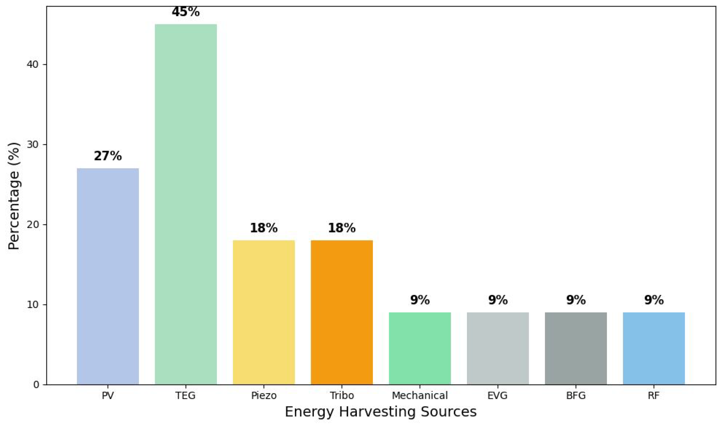
Figure 1. Multi-source energy harvesting concept: Idea and key advantages.
Electronics 14 01951 g001
Figure 2. Generalized model of multi-source energy harvesting system.
Electronics 14 01951 g002
Figure 3. AC to DC and DC to DC conversion circuits of an energy harvesting system.
Electronics 14 01951 g003
Figure 4. Categorization of energy harvesting sources and working principles.
Electronics 14 01951 g004
Figure 5. Complementary energy harvesting architecture.
Electronics 14 01951 g005
Figure 6. PowerOring energy harvesting architecture.
Electronics 14 01951 g006
Figure 7. LDO’s summation energy harvesting architecture.
Electronics 14 01951 g007
Figure 8. Shared-inductor energy harvesting architecture.
Electronics 14 01951 g008
Figure 9. Dual Input systems block diagram.
Electronics 14 01951 g009
Figure 10. Dual Input systems-energy harvesters type exploitation.
Electronics 14 01951 g010
Figure 11. Dual Input systems-maximum output power for connected loads and peak efficiency [40,41,42,43,44,45,46,47,48,49].
Electronics 14 01951 g011
Figure 12. FoM comparison of state-of-the-art dual input energy harvesting systems [40,41,42,43,44,45,46,47,48,49].
Electronics 14 01951 g012
Figure 13. Multi-input systems-block diagram.
Electronics 14 01951 g013
Figure 14. Multi-input shared inductor systems-energy harvesters type exploitation.
Electronics 14 01951 g014
Figure 15. Multi-input shared inductor systems-maximum output power for connected loads and peak efficiency [37,38,50,51,52,53,54,55,56,57,58,59,60,61].
Electronics 14 01951 g015
Figure 16. FoM comparison of state-of-the-art multi-input shared inductor energy harvesting systems [37,38,50,51,52,53,54,55,56,57,58,59,60,61].
Electronics 14 01951 g016
Figure 17. Fully-integrated simultaneous energy harvesting approach.
Electronics 14 01951 g017
Figure 18. Silicon integrated energy harvesting systems published per year and per process node.
Electronics 14 01951 g018
Table 1. Energy Harvesting Technologies: Power Density and Indicative Applications.
Energy Harvesting TechnologyType/MaterialPower Density (μW/cm−2)Indicative Application
Organic Solar Cells [20]P3HT: ICBA22.57 (@ 500 lux)Fluorescent light indoor energy harvesting (e.g., office)
PTB7:PC71BM (0.15 cm2)15.487 (@ 500 lux)LED lamp indoor energy harvesting
PM6:PC71BM (1 cm2)54.69 (@ 300 lux)dim indoor light harvesting
Micro-TEGs 1 [21]Bi0.5Sb1.5Te3/Be2Te2.4Se0.6 thin-film0.0016Sensor power up (IR sensors, flow sensors, power sensors)
Bi2Te3-based flexible0.0026Human body applications
Silicon-based monolithic planar0.000032wearables
Microbial Fuel Cells [22]Deltaproteobacterium1.4Low-power marine sensors power up
Gammaproteobacteria, Shewanella affinis3.6Biocatalytic fuel cells for medical or environmental biosensing
Betaproteobacteria4.0 ± 0.2Bio-batteries or lab-on-a-chip systems for microelectronic or wearable devices
Piezoelectric Transducers [17]PVDF-Ce-G0.56Pressure based energy harvesting
PVDF-Er3+/Fe3+76.8Capacitor charging
PVDF-TrFE-BT NPs5.05Biomechanical energy harvesting
Triboelectric Nanogenerators [23]Fiber-based8.5Wearable energy harvesting
All-fiber70Smart textiles and self-powered sensors
Textile-based0.1Wearable devices, motion sensors
Radio Frequency [24]Radio GSM0.1Low-power sensors, wearable trackers, asset tags in urban environments
WiFi0.001Passive RFID-like sensors, smart home buttons, ultra-low-power IoT devices
1 The power density for TEGs is measured in W / cm 2 K 2 .
Table 2. A comparison of state-of-the-art dual input energy harvesting systems.
Ref.YearProcess (nm)Input TypeNo. LoadVin RangePout Max (mW)Peak EfficiencyArea (mm2)External ComponentsBattery
[39]2014350PV, mechanical10.2–1.7 Vn/a73%4Cload, L (values n/a)yes
[40]2015500 V CMOSBattery, PV1PV: 40 μW1593%0.79L = 10 μ H, CPV = 4.7 μ F, Co = 4.7 μ Fyes
[41]2016350PV, Battery31 V Voc3485%4L = 22 μ H, Cin = 4.7 μ F, Cout = 4.7 μ Fyes
[42]2017180BFC, TEG2TEG: 10–90 mV, BFC: 26–250 mV2.385.2% TEG, 90.4% GBFC, 89.5% Combined2.3L = 100 μ H, CIN1 = 4.7 μ F, CIN2 = 10 μ F, CST = 100 nF, CCTRL = 30 nF, switchno
[43]2018180Piezo, TEG1PZT: 0.6 V, @ 140 Hz TEG: 0.1–0.5 V0.4575%1.5L = 680 μ Hyes
[44]2020180EVG, TEG1EVG: 0.5–1 Vp, TEG: 25–100 mV0.11982%0.83CIN = 1 μ F, CTEG = 0.1 μ F, C12 = 7.6 μ F, COUT = 10 μ F, L = 1 mHyes
[45]2020180 BCDTribo × 2170 V0.0152.90%2.482R = 30 GOhm × 4, L = 1 mH × 1, C = 5 μ F × 5no
[46]2020180 BCDTribo × 21<70 V0.04275.60%1.694L = 10 mH, C = 1 μ F × 2yes
[47]2021180RF × 21915 MHz0.0375.20%0.085Cb = 1 nF × 2, Cs = 1 μ F, L = 10 μ Hyes
[48]2023180TEG, Battery1TEG: 0.1–0.6 V, Battery: 1.5 V31.590.48%2.531R = 0.3 Ohm, R_LDO = 84 MOhm, R = 40 MOhmyes
[49]2024180 BCDTEG, Piezo (aux)1PZT: 1.8 Vp @ 280 Hz, TEG (DC emulation) 10–100 mV0.4463.90%0.4L = 220 μ H, Rldo1 = 84 MOHm, Rldo2 = 40 MOhm, Cbuf = n/ano
Table 3. A comparison of state-of-the-art shared inductor multiple input energy harvesting systems.
Ref.YearProcess (nm)Input TypeNo. LoadVin RangePout Max (mW)Peak EfficiencyArea (mm2)External ComponentsBattery
[38]2012350PV, TEG, Piezo2TEG: 20 mV–0.16 V, PV: 0.15–0.75 V, Piezo: 1.5–5 V1058% TEG, 83% PV, 79% Piezo25L = 22 μ H, C = 15 μ F, CPV = 47 μ F, CTEG = 94 μ F, CPz = 1 μ Fyes
[50]2015320 BCDPiezo, TEG, PV, RF1PZ: 0.7–5 V, LV: 0.1–1 V, HV: 1–5 V2.1289.60%4.6CST = 66 μ F, L = 10 mH, CbHV1 = 2.7 μ F, CbLV = 22 μ Fno
[51]2015180PV, Battery3PV: 1.5 V, Vbat: 2.5 V1083%4.62L = 10 μ H, 4 × C = 10 μ Fyes
[52]2016180PV, Piezo, RF1PV: 0.2–1.2 V, RF, Piezo n/a984%1.1L = 44 μ H, CB = 10 μ F, CD = 10 μ F, Cstore = 100 μ Fno
[53]201640TEG, RF1RF 100 μW–5 mW, TEG: 50–300 mV3685.5% TEG, 93.8% RF1.38CIN1 = 4.7 μ F, CIN2 = 22 mF, CSTO = 2.6 mF, CL = 47 μ F, LLTO = 8.2 μ Hno
[37]201828 FDSOIPV, TEG, BFC, Battery4PV: 0.2–1 V, TEG: 0.1–0.4 V, BFC: 0.2–0.5 V, Battery: 1.8 V6089%0.510 μ H, Cout = 1 μ Fyes
[54]2018180PV, Piezo9n/a12071.90%5.29L, Cout (values n/a)yes
[55]2018180PV, TEG, Storage3PV: 0.4–0.8 V, TEG: 0.05–0.3 V484.40%1.84 L = 4.7 μ H, CPV/CTEG = 10 μ F, COUT1 = 1 μ F, COUT2 = 1 μ F, COUT3 = 100 μ Fno
[56]2019180PV × 2, TEG10.1–0.8 V1082%0.75L = 4.7 μ H, CPV1/CPV2 = 0.1 μ F, CTEG = 1 μ F, COUT = 10 μ F, CSTO = 100 μ Fno
[57]2019180PV, Battery2PV: 0.55–0.7 V, Vbat: 1.4 V1.292.50%2.4154.7 μ H, Caps × 2 (value n/a)yes
[58]2021180RF × 22240–440 mVn/a85%n/aL = 47 μ H, CH1 = 2 μ F, CH2 = 1 μ F, CL1 = 10 μ F, CL2 = 100 μ F, CSTO = 100 μ Fno
[59]2021180PV, TEG, BFC3PV: 1.45–1.8 V, BFC: 0.2–0.7 V, TEG: 0.03–0.09 V2490.20%2.58L = 4.7 μ H, Cin = 10 μ F, Cout = 2.2 μ Fyes
[60]2023180PV, TEG, Piezo, PEG, MEG, RF3PV1: 2–5 V, PV2: 20–120 mV, TEG/BFC: 0.03–0.5 V, PEG/MEG: 1.8–5 V, RF: 2–5 V132.692.50%1.92L = 80 μ H, SCs = 22 mFyes
[61]2023180Piezo × 2, TEG, PV1PZT × 2: 0.5–2 V, TEG: 0.05–0.4 V, PV: 0.2–1.5 V584% PV, 76% TEG, 76.5% PZT0.9L = 470 μ H, CPV = 4.7 μ F, CTEG = 22 μ F, CSTO = 22 μ F, Csamp = 1 nFno
Table 4. A comparison of state-of-the-art fully-integrated multiple input energy harvesting systems.
Ref.YearProcess (nm)Input TypeNo. LoadVin RangePout Max (mW)Peak EfficiencyArea (mm2)External ComponentsBattery
[62]2019180DC-like emulation125 μ W to 600 μ W0.555%n/anoneno
[63]2023180TEG, RF2DC: 300 mV, RF: −2 dBm1.27560.30%3.33noneno
Disclaimer/Publisher’s Note: The statements, opinions and data contained in all publications are solely those of the individual author(s) and contributor(s) and not of MDPI and/or the editor(s). MDPI and/or the editor(s) disclaim responsibility for any injury to people or property resulting from any ideas, methods, instructions or products referred to in the content.

