Article

The Influence of the Design of Antenna and Chip Coupling Circuits on the Performance of Textronic RFID UHF Transponders

by
Anna Ziobro
1,*,
Piotr Jankowski-Mihułowicz
2,*,
Mariusz Węglarski
2 and
Patryk Pyt
2
1
Doctoral School of the Rzeszów University of Technology, 35-959 Rzeszów, Poland
2
Department of Electronic and Telecommunications Systems, Rzeszów University of Technology, Wincentego Pola 2, 35-959 Rzeszów, Poland
*
Authors to whom correspondence should be addressed.
Electronics 2024, 13(9), 1759; https://doi.org/10.3390/electronics13091759
Submission received: 29 March 2024 / Revised: 27 April 2024 / Accepted: 30 April 2024 / Published: 2 May 2024
(This article belongs to the Special Issue RF/Microwave Device and Circuit Integration Technology)

Abstract

:
The objectives of this study were to design, investigate, and compare different designs of coupling circuits for textronic RFID transponders, particularly focusing on magnetic coupling between an antenna and a chip. The configuration of the inductively coupled antenna module and the microelectronic module housing the chip can be varied in several ways. This article explores various geometries of coupling circuits and assesses the effects of altering their dimensions on mutual inductance, chip voltage, and the transponder’s read range. The investigation comprised an analytical description of inductive coupling, calculations of mutual inductance and chip voltage based on simulation models of transponders, and laboratory measurements of the read range for selected configurations. The results obtained from this study demonstrate that various designs of textile transponders are capable of achieving satisfactory read ranges, with some configurations extending beyond 10 m. This significant range provides clothing designers with the flexibility to select transponder designs that best meet their specific aesthetic and functional requirements.

1. Introduction

1.1. Textronic UHF RFID Transponders

The integration of RFID technology in clothing has gained significant interest among researchers. This field is a key area in the development of IoT systems, which have become increasingly prevalent and accessible in everyday life in recent years [1]. However, developing textile UHF RFID transponders introduces unique challenges not seen in other applications. These transponders need to be as flexible as the textile materials and withstand the mechanical stresses that occur during garment use, such as bending and stretching. Additionally, they must be durable enough to handle garment maintenance processes and environmental conditions related to close contact with the human body, including temperature and humidity changes [2,3].
In the literature, e-textile UHF RFID tags predominantly feature antennas embroidered with conductive threads [4,5,6,7,8,9,10,11,12]. Notably, a knitted transponder was discussed in reference [13]. These transponders vary in their antenna types, impedance matching elements, substrates, and threads. Researchers have proposed various antenna structures, such as dipole, meander line, rectangular, octagonal, fractal geometries, slotted patches, and two symmetrical circular patches. Some unique designs even include text-meandered and Mickey Mouse-shaped antennas. Challenges related to the use of conductive threads have also been addressed, focusing on issues like yarn deformations, reproducing the designed structure accurately, machine settings, and methods used to measure the conductivity of embroidered antennas [12,14,15,16].
Various techniques and materials are used to fabricate textile RFID transponders. For instance, references [17,18,19,20] described transponders made from flat conductive materials that are adhered or pressed onto the fabric. Additionally, conductive inks and printing techniques have been employed [21,22,23,24,25]. Research has also investigated the use of graphene for textile antennas, utilizing methods like laser-induced graphene or specially created materials such as flexible graphene assembly films and conductive pastes [26,27,28,29,30,31,32]. Graphene is favored in textile RFID transponders for its flexibility, high conductivity, and mechanical strength. However, adopting new materials and techniques introduces challenges not previously encountered in the textile industry, such as increased costs, process complexity, potential toxicity, and limitations in washability [33,34].
Some studies have investigated the use of textile RFID transponders as sensors, exploring applications such as strain sensors [17], surface crack monitors [35], and handwriting sensors [36].
In the design of textile RFID transponders, ensuring a reliable galvanic connection between the antenna and the chip is critical, especially for wearable devices. Traditional soldering methods are often unsuitable for textile materials because of the high temperatures required [37]. Alternatives such as low-temperature soldering [34], adhesive bonding with conductive epoxy [4,8,12,19,20], and various mechanical connections have been explored. Mechanical connections include sewing, snap buttons, and insertion methods as discussed in reference [37]. Additionally, embroidered [6,38] and knitted [13] interconnections have been proposed, and the authors of [7] introduced chipless, embroidered RFID transponders.
A novel approach employing inductive coupling between the antenna and chip, as opposed to traditional galvanic coupling, has been explored in textronic UHF RFID transponders, first introduced in reference [39]. This method was developed to address the integration challenges of embedding microelectronic components directly into textile materials. With inductive coupling, the microelectronic assembly, which includes the chip and its coupling system, can be manufactured using conventional techniques and subsequently attached to clothing as typical functional or decorative elements, such as buttons. Although research has already been conducted on such transponders regarding the factors that condition their operation [40,41,42] and their application possibilities in IoT systems [43,44], the potential for designing various configurations of coupling circuits has not been considered.
This concept of physical separation between the antenna and the chip has also been investigated in study [5], though with a different objective. In this research, the transponder functions as a displacement and strain sensor, where its operational capability is derived from changes in the coupling between its components. Unlike the approach in reference [39], the chip coupling circuit in study [5] was embroidered, presenting ongoing challenges in seamlessly integrating textile materials with electronic chips. Additionally, the possibility of designing the coupling system in various ways was not considered. Consequently, no studies were found that proposed, investigated, or compared the coupling quality of different configurations of the coupling system in textile RFID transponders.

1.2. The Aim of This Research

The objectives of the study were to design, investigate and, compare various constructions of coupling circuits in textronic UHF RFID transponders, with a specific focus on optimizing inductive coupling. This research represents a significant advancement in the development of textile transponders, moving away from traditional galvanic connections and toward a magnetic coupling approach. Previous studies by the authors have extensively investigated various aspects of these transponders, including the impact of the textile substrate [40], effects of washing processes [41], resistivity of conductive threads, and production inaccuracies, and provided a comprehensive mathematical description of the transponder’s function [42]. These studies have also involved comparisons of different methods for determining the mutual inductance between the antenna and chip coupling circuits [42]. However, until now, all research has been confined to a single coupling circuit design, which utilized a one-loop antenna coupled with a two-loop chip circuit.
The innovative aspect of the proposed textile transponder is its elimination of the galvanic connection between the antenna and the chip. Instead, inductive coupling is used, which depends on the design of the antenna and chip coupling circuits, including their sizes, shapes, and relative positions.
The textronic UHF RFID transponder consists of two main components: an antenna module, which includes an embroidered antenna and its coupling circuit, and a microelectronic module, which contains the chip and its coupling circuit. A prototype featuring an embroidered dipole antenna and a square-shaped chip coupling circuit is shown in Figure 1.
The production of the antenna and its coupling circuit typically involves embroidery, although alternative conductive materials can be used. It is vital that the fabrication methods align with standard textile industry practices. The lack of a galvanic connection also allows the transponder production to be split into two stages. Initially, the microelectronic circuit is manufactured and can be sent to sewing workshops or tailoring studios. There, the final assembly of the transponder is completed, involving the embroidery of the antenna and integration of the microelectronic module into the garment.
This article will explore four diffrent designs of transponders where the antenna is linked to the chip through inductive coupling. Each design varies in the construction of the antenna and chip coupling circuits, responding to the need to improve the transponder performance and accommodate the specific demands of the apparel industry. Such designs allow for the microelectronic module to be either discreetly integrated into the garment’s functional elements or prominently displayed as part of its decoration. Clothing designers are given the flexibility to choose a design that best meets the project’s requirements, considering factors like garment type, aesthetic appeal, material choice, and wearer comfort.
The first design category of textronic transponders features coupling circuits that are stacked directly on top of each other (illustrated in Figure 2). This stacked, flat configuration has been previously employed and examined in studies on RFIDtex tags [39,40,41,42], where the antenna’s coupling circuit was a single loop, and the chip’s coupling circuit comprised two loops, with the outer loop’s diameter aligning with that of the antenna. This article introduces various new proposals for these planar coupling circuits.
An alternative design approach eliminates the antenna coupling circuit and positions the microelectronic module near the radiator, as illustrated in Figure 3. The chip coupling circuit is placed within the magnetic field generated by the radiator. Although this configuration results in weaker inductive coupling due to the absence of a dedicated antenna coupling circuit, it simplifies manufacturing. If the resulting read range is adequate, this streamlined construction might be preferred due to its ease of production.
Previous studies [42] have shown that even minor misalignments on the order of millimeters between the antenna and chip coupling circuits can significantly reduce the read range. This problem can be addressed by designing the antenna coupling circuit to also secure the chip coupling circuit to the garment. In this design, the conductive thread is wound around the chip coupling circuit’s paths and sewn into the fabric, as depicted in Figure 4. However, this approach carries a risk: the antenna coupling circuit might be designed or installed in a way that, although it ensures that the microelectronic system is permanently attached to the garment through the conductive thread, it may not effectively transfer energy between the antenna and the chip. The correct technique for wrapping the chip coupling circuit with the conductive thread, in accordance with the principles of electromagnetism, will be explored in greater detail in the subsequent sections of this article.
The final proposal suggests adding a core to the transponder’s construction, where both the antenna and chip coupling circuits will be mounted. In this design, conductive thread is wound around the core to form a coil, as illustrated in Figure 5. Increasing the number of coil turns boosts the magnetic flux in the circuit, which is expected to enhance inductive coupling. This improvement is particularly beneficial for transponders where the dimensions of the coupling circuits or the conductivity of the thread do not allow for a satisfactory read range.
The article will offer an analytical description of inductive coupling, complemented by numerical calculations for each proposed group. Additionally, experimental studies were conducted to evaluate the read range of selected designs from the first two groups. These studies helped validate the theoretical models and provided practical insights into the performances of these transponders.
The structure of this article is organized as follows. Initially, the research topic is introduced with a brief overview of the mathematical model of the transponder, specifically focusing on the challenge of determining mutual inductance within its coupling system, as elaborated in publication [42]. The subsequent four sections delve into numerical simulations conducted for various models, categorized by their types of transponder coupling systems. In these sections, both the mutual inductance and chip voltage for each model are discussed. Finally, this article presents the results of laboratory measurements, detailing the read range achieved by the transponders.
For the first group of transponders with planar coupling systems, simulations were conducted for transponders with circular and square coupling layouts. For circular layouts, the impact of adding internal loops to the largest chip coupling system with a diameter of 5.7 mm was assessed. These designs were also constructed, and their read range was measured. For square configurations, the effects of changing their sizes from 5.7 mm to 50 mm on their mutual inductance and chip voltage were investigated.
For systems without an antenna coupling arrangement, numerical calculations were performed for square and rectangular layouts. The dimensions of the square modules ranged from 5.7 mm to 50 mm. For the rectangular ones, the longer side varied within the same range, while the shorter side was consistently 5.7 mm. The rectangular configurations were positioned both parallel and perpendicular to the antenna with the longer side. Selected models were constructed, and their read ranges were measured.
In the group of transponders with antenna coupling circuit wrapping around chip coupling circuit, only numerical models were created. Each design utilized a square chip coupling layout with a side length of 11.4 mm. Variations included different methods of wrapping the conductive thread around the chip, altering its position relative to the paths and the number of knots.
For transponders with a core, only numerical calculations of mutual inductance and chip voltage were conducted. These models explored the effects of variables such as the number of turns, the spacing between turns, the sequence of placing circuits on the core, and the core material. Each model employed a single-loop chip coupling system with a diameter of 5.7 mm.

2. Materials and Methods

This study involved analytical calculations based on common electromagnetic laws. A mathematical model of the transponder was utilized to determine the mutual inductance between the coupling circuits and the chip voltage based on the results of numerical calculations [42]. The transponder models were constructed and simulated using EMCoS Studio software, following simulation methodologies from previous studies [40]. The simulation provided impedance values for the embroidered antenna module, the chip coupling circuit, and the transponder antenna. Matlab was used for calculations and graphical representation of the results.
In all simulated transponder models, the use of conductive thread PACKLitzWire 10 × 0.04 mm, 2 × 52 was assumed. This thread comprises intertwined copper wires insulated with silk. In the model, the conductor thickness was defined as 93 μm, and the insulation as 35 μm. A relative dielectric constant of 3 was assumed for silk. The model was augmented with a substrate simulating textile material with a thickness of 0.66 mm, a relative permittivity of 1.53, and a dielectric loss of 0.0051. These parameters were measured for a real sample of fabric consisted of 82% polyester and 18% spandex. This fabric is suitable for t-shirts or casual dresses. The parameters of the substrate on which the traces of the microelectronic circuit were made were as follows: a thickness of 152 μm, a dielectric constant of 2.855, and a dielectric loss of 0.11. Between these two substrates, there was a layer of air with a thickness of 256 μm.
The selected models were fabricated, and their operating ranges were measured. The antennas were sewn using an embroidery machine, BROTHER INNOV-IS V3. Agsis Syscom conductive thread was used. The microelectronic circuits were fabricated on a Kapton substrate. The NXP Semiconductors Ucode 7m SL3S1214 chip was utilized. Read range measurements were conducted in a Microwave Vision Group anechoic chamber equipped with a Voyantic Tagformance Pro measurement system with Tag-formance UHF v.13.2.3 software. Reader parameters set in Voyantic software is shown in Figure 6.

3. Results

3.1. Calculations and Simulations

3.1.1. Mathematical Model of Textronic UHF RFID Transponder

The foundational mathematical model of the transponder, which includes both the chip and antenna coupling systems, was extensively detailed in publication [42]. In this paper, we focus only on the most crucial information from that model that underpins the ongoing research.
The electrical equivalent of the radiofrequency frontend in the textronic UHF RFID transponder is depicted in Figure 7.
The left circuit refers to the antenna module, which physically consists of an embroidered antenna (half-wave dipole) and its coupling circuit. The right circuit represents the microelectronic module, containing the chip coupling circuit and the chip. Both circuits are magnetically coupled. It should be explicitly noted that the embroidered antenna module is not identical to the transponder antenna, which is highlighted on the diagram with a red border. The transponder antenna consists of an embroidered antenna connected through inductive coupling to the chip coupling circuit.
The physically constructed antenna module comprises the radiator and the coupling circuit. Its impedance can be described by the following formula:
Z A = R A + j X A
where R A represents the resistance, and X A represents the reactance.
The right circuit is the microelectronic module, comprised of a chip and its coupling circuit. The impedance of the chip coupling circuit can be expressed as follows:
Z CM = R CM + j X CM
where R CM represents the resistance, and X CM represents the reactance.
The inductive coupling between the antenna and chip coupling circuits can be described using the mutual inductance coefficient M. The impedance Z M contains only the imaginary part X M :
Z M = j X M = j ω M
where ω represents the angular frequency.
The presented electrical circuit can be represented by a two-port network as it resembles the circuitry of an air-core transformer. Using the equivalent circuit, formulas for the impedance of the transponder antenna Z TA , and the chip voltage U TC can be derived:
Z TA = Z CM + X M 2 Z A
U TC = I CM Z TC = U A j X M Z TC Z A ( Z CM + Z TC ) + X M 2
where I CM is the microelectronic module current, U A is the antenna module voltage, Z TC is the chip impedance.
The quality of the inductive coupling is crucial for the operation of the transponder because it determines the amount of energy transferred to the microelectronic circuit. The read range of the transponder depends on the power delivered to the chip. The power is determining by the chip voltage, which, according to Equation (5), reaches a maximum for a certain value of X M . Thus, the efficiency of the operation of various transponder coupling circuit designs can be estimated by comparing their mutual inductance coefficients. However, determining this value poses an issue, as numerical software lacks a direct function for calculating it.

3.1.2. Mutual Inductance between Coupling Circuits

The issue of determining mutual inductance was also addressed in publication [42], where various methods were discussed and compared with each other. One of the methods used to determine the value of X M for the investigated transponder construction is to utilize Equation (4). After rearranging the equation, the following formula is obtained:
X M = ( Z TA Z CM ) Z A
This value can also be obtained using known analytical electromagnetic formulas. The mutual inductance coefficient between two circuits is defined as the ratio of the magnetic flux Φ 12 generated by the first circuit passing through the second circuit to the current I 1 generated by the first circuit [45]:
M 12 = Φ 12 I 1
The magnetic flux is described by formula [45]:
Φ 12 = S Bds = S Bds cos α
where B is the magnetic flux density, S is the area passed through by the flux, and α is the angle between their vectors. The value of B can be calculated using the Biot–Savart law. If the magnetic flux passes through a circuit with z coils, then the formula for the flux linkage is obtained [45]:
Ψ 12 = z Φ 12
In this case, the mutual inductance coefficient is determined as follows [45]:
M 12 = Ψ 12 I 1
Assuming that reactance is proportional to frequency, the relationship between M and X M can be expressed as follows:
X M = j 2 π f M
As demonstrated in reference [42], analytical formulas can be applied to estimate the value of X M for transponders with antennas of uncomplicated geometry. Therefore, dipole antennas were utilized in the transponders presented in this study.

3.1.3. Transponders with Planar Chips and Antenna Coupling Circuits

The primary function of the antenna coupling circuit is to facilitate energy transfer between the antenna and the microelectronic module. In addition to this, the antenna radiator itself generates a magnetic field, contributing to the overall field of the coupling circuit. Thus, the magnetic flux around the chip coupling system is the result of both the antenna coupling circuit and the radiator.
Previous research on textronic UHF RFID transponders commonly examined designs featuring a loop antenna coupling circuit paired with a two-loop chip coupling circuit. Incorporating an additional loop into the coupling circuit increases the mutual inductance, with the mutual inductance coefficient, M, being the sum of the inductance coefficients from each loop of the antenna coupling circuit. The equation for this is
M AC = M 1 L + M 2 L
where M AC represents the total mutual inductance coefficient between the antenna module and the chip coupling circuit. Here, M 1 L is the mutual inductance coefficient between the first loop of the chip coupling circuit and the antenna, and M 2 L corresponds to the mutual inductance between the second loop and the antenna.
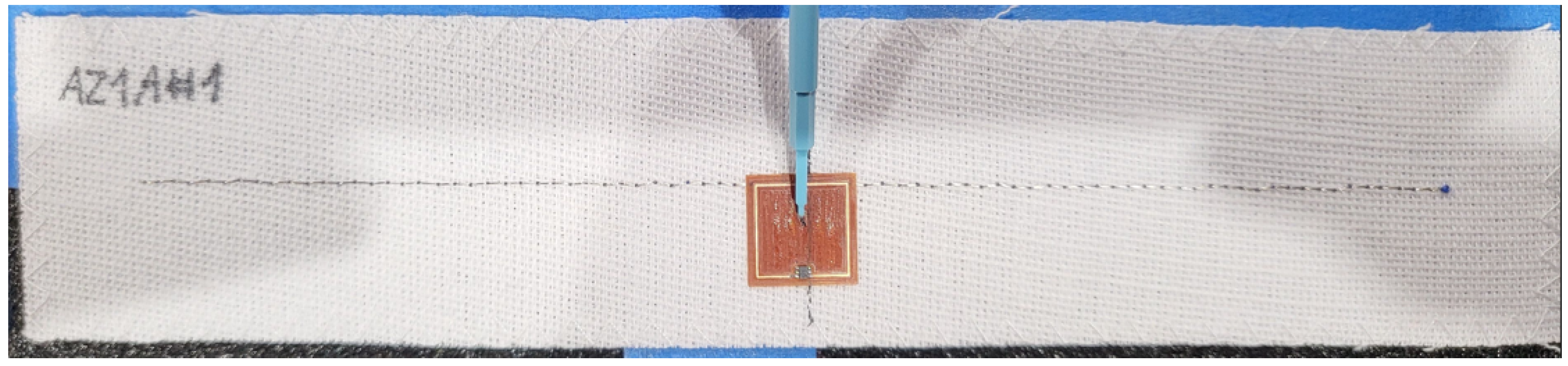
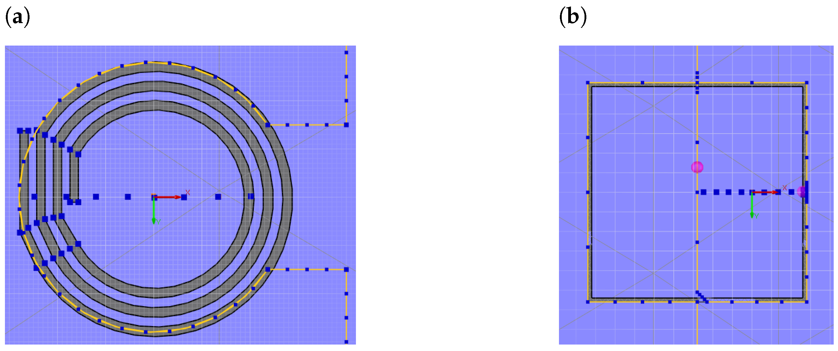
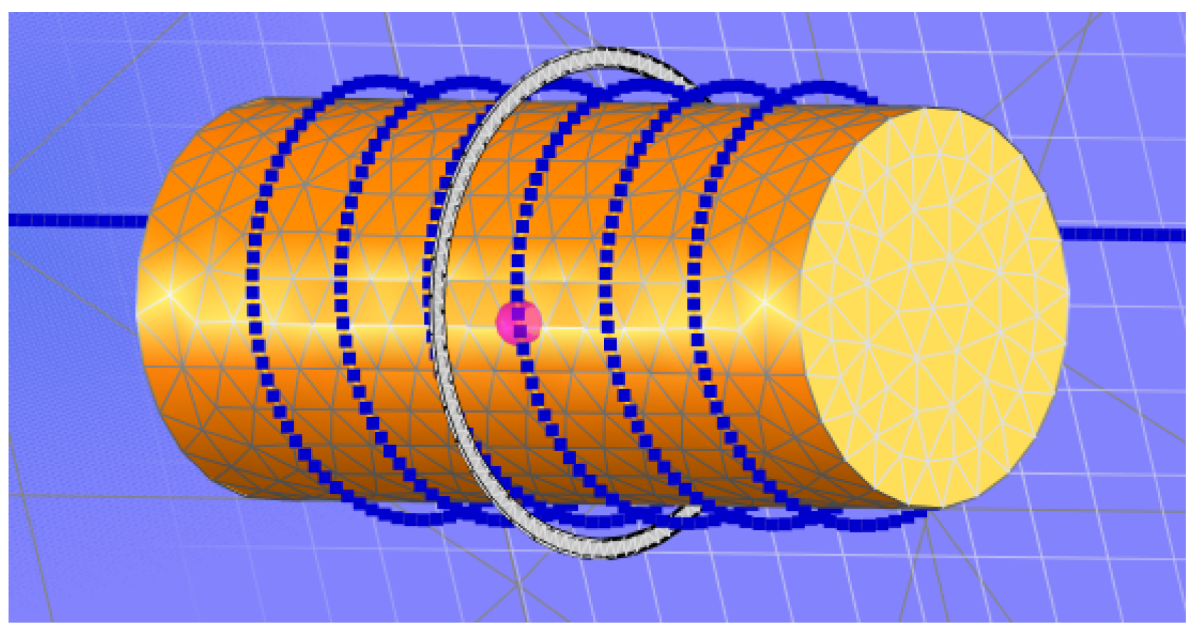
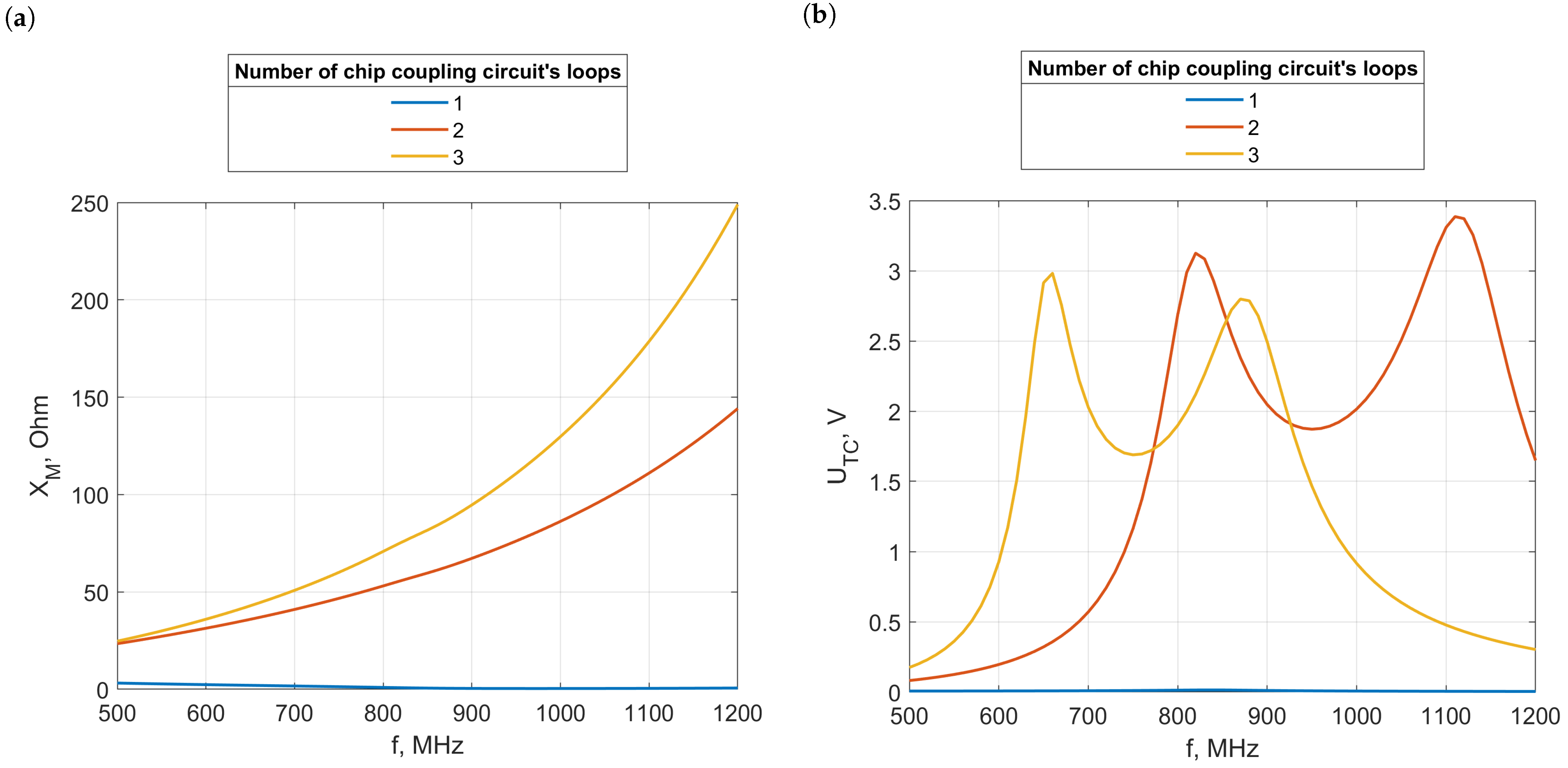
The numerical and experimental impacts of adding additional loops to the chip coupling circuit have been thoroughly investigated. Three chip coupling circuits were designed, each featuring an outer loop diameter d = 5.7 mm, a track width of 0.2 mm, and a loop-to-loop spacing of 0.2 mm (Figure 8). For each simulation, an antenna coupling circuit was configured as a circle with a diameter of 5.7 mm (Figure 9). The antenna’s radiator was designed with a length of 160 mm.
Section 2 describes the parameters of the transponders modeled in EMCoS Studio. Using Equations (5) and (6), along with the numerically calculated impedances of the transponder antenna Z TA , embroidered antenna Z A , and chip coupling circuit Z CM , the mutual inductance X M and chip voltage U TC were calculated (Figure 10). Each simulation assumes that an antenna module is U A = 1 V and a chip impedance of Z TC = 15.3 313 i   Ω . The calculations span frequencies from 0.5 to 1.2 GHz. This broad frequency range was chosen to explore how variations in coupling circuits affect antenna resonance and the frequency shift of the maximum chip voltage U TC . The studies presented here are preliminary, conducted under the assumption that future methods will be developed to adjust antenna arm lengths to manipulate the position of the maximum U TC on the frequency axis. At this stage, the focus is not on the practical applicability of transponders in designated RFID bands but on understanding the underlying principles.
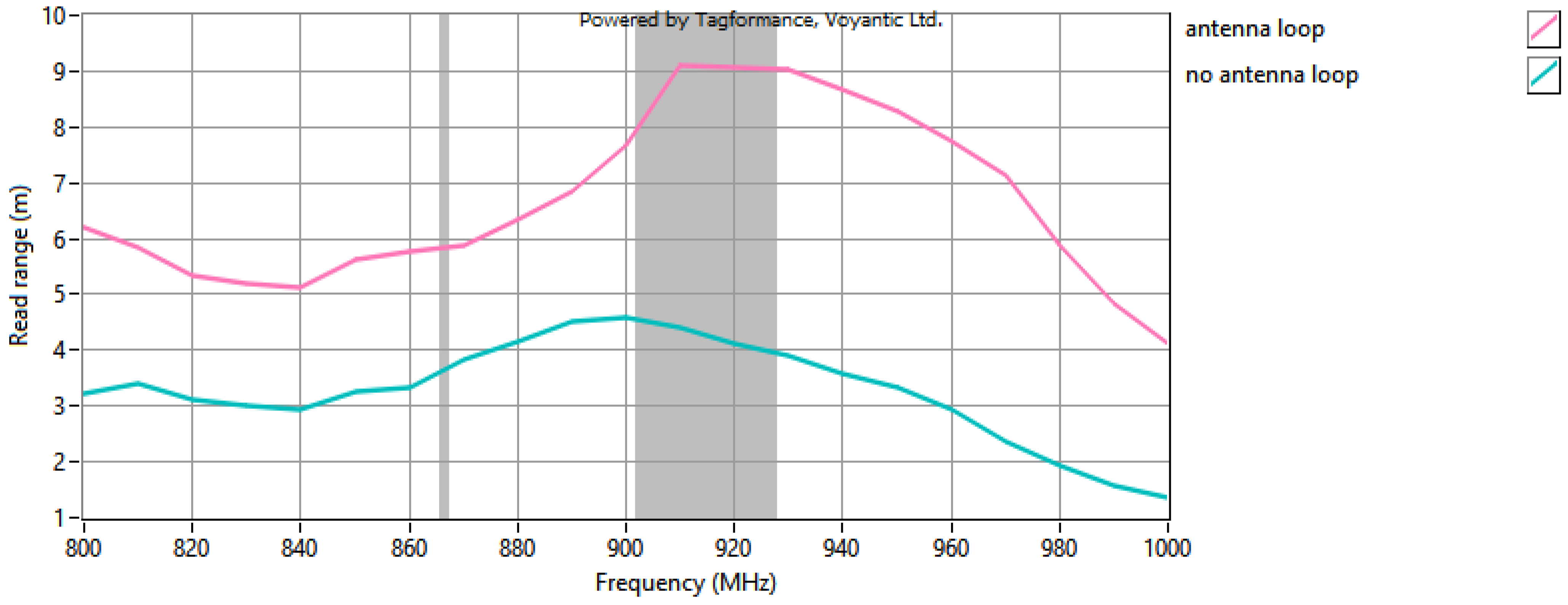
The results highlight significant differences in performance across the configurations. For the single-loop design, the maximum mutual inductance X M achieved was 3.19 Ω , with a chip voltage U TC of 0.014 V. Introducing a second loop markedly improved the inductive coupling between the circuits. However, adding a third loop only slightly increased X M and paradoxically reduced the voltage, indicating that it surpassed the optimal value for this transponder design. This addition also caused a noticeable shift in the maximum on the frequency axis and a narrowing of the operational frequency range.
In this setup, the loops are placed a few millimeters from the antenna arms, simplifying the embroidery process. Nonetheless, the greater distance from the radiator weakens the magnetic induction, leading to reduced inductive coupling. To address this issue, square-shaped antenna and chip coupling circuits were used, enhancing the coupling efficiency. 
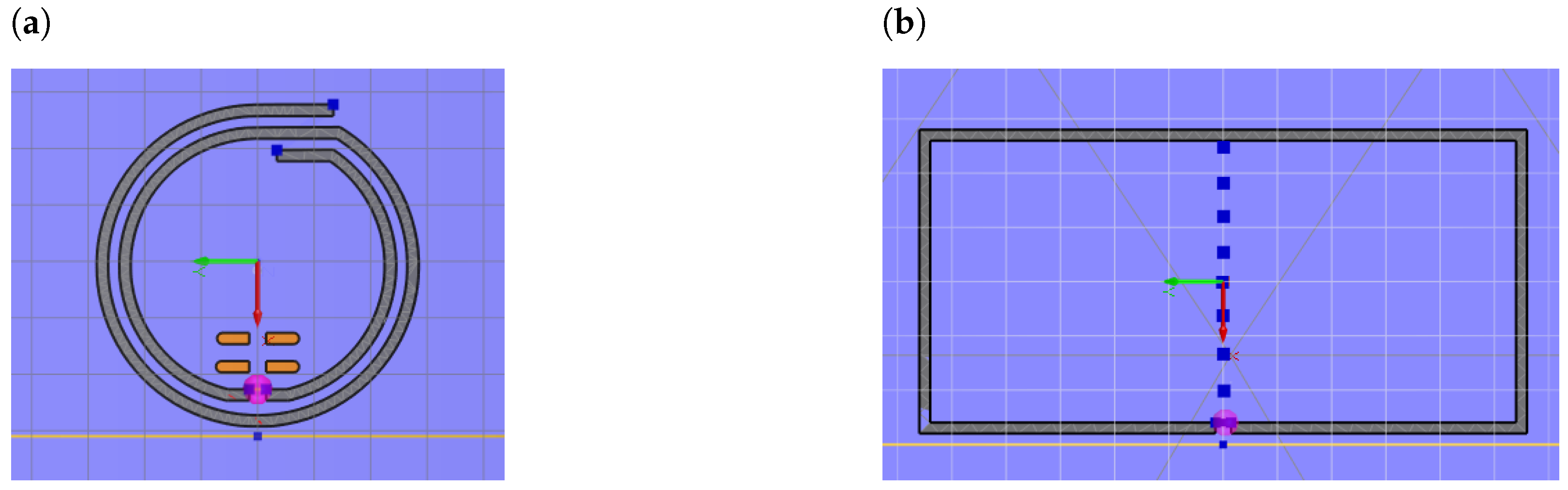
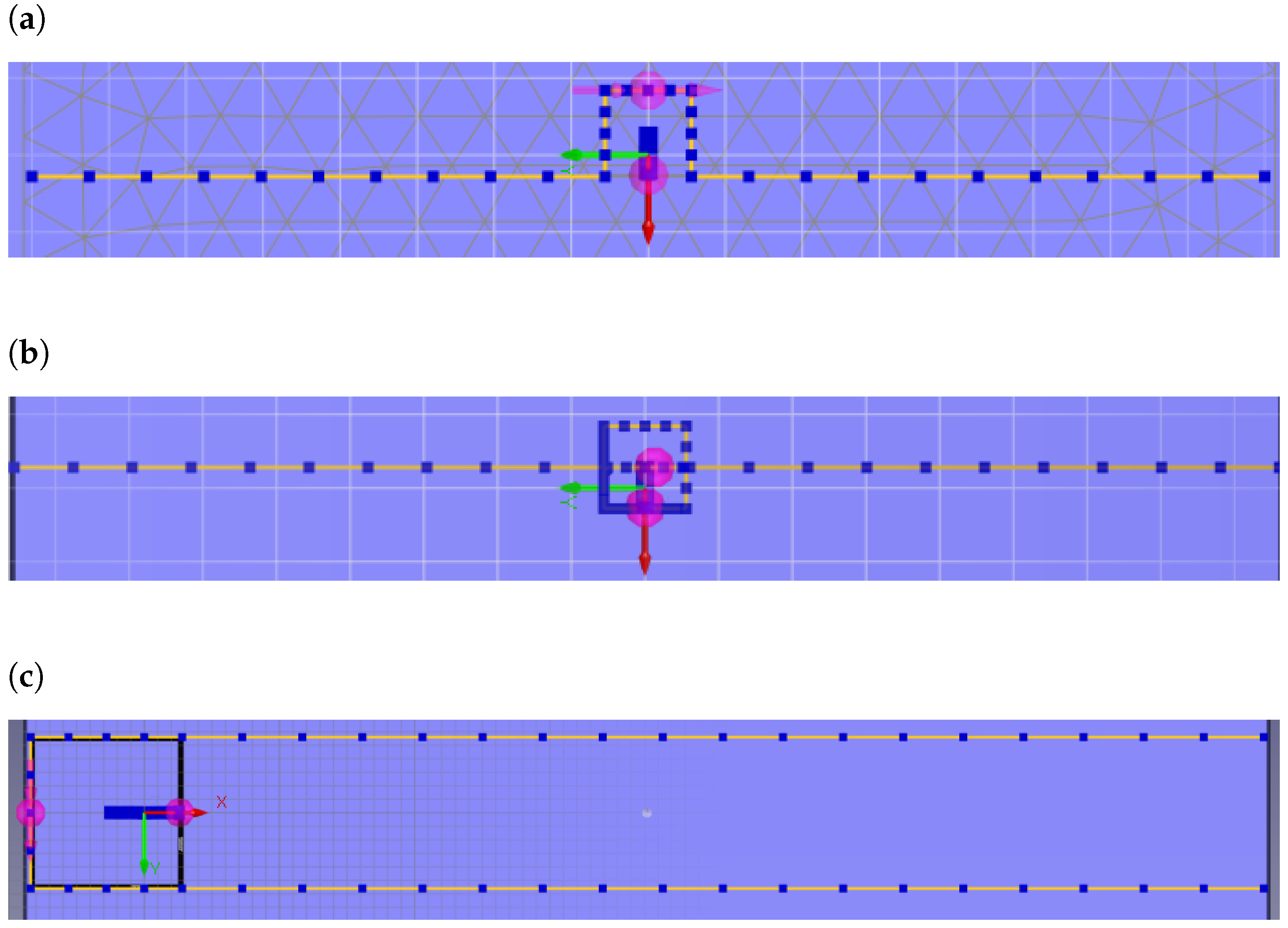
Figure 11 illustrates three different geometries of the embroidered antenna paired with a square coupling circuit.
The first geometry adapts the previously explored circular coupling circuit into a square shape, but with only three embroidered sides. The second design features a fully embroidered square, necessitating a change in the placement of the antenna arms to accommodate the new shape. Specifically, the arms are aligned with the center of the square, with one arm passing through the square’s area. The third design adopts a U-shaped antenna, where the bend itself functions as the coupling circuit.
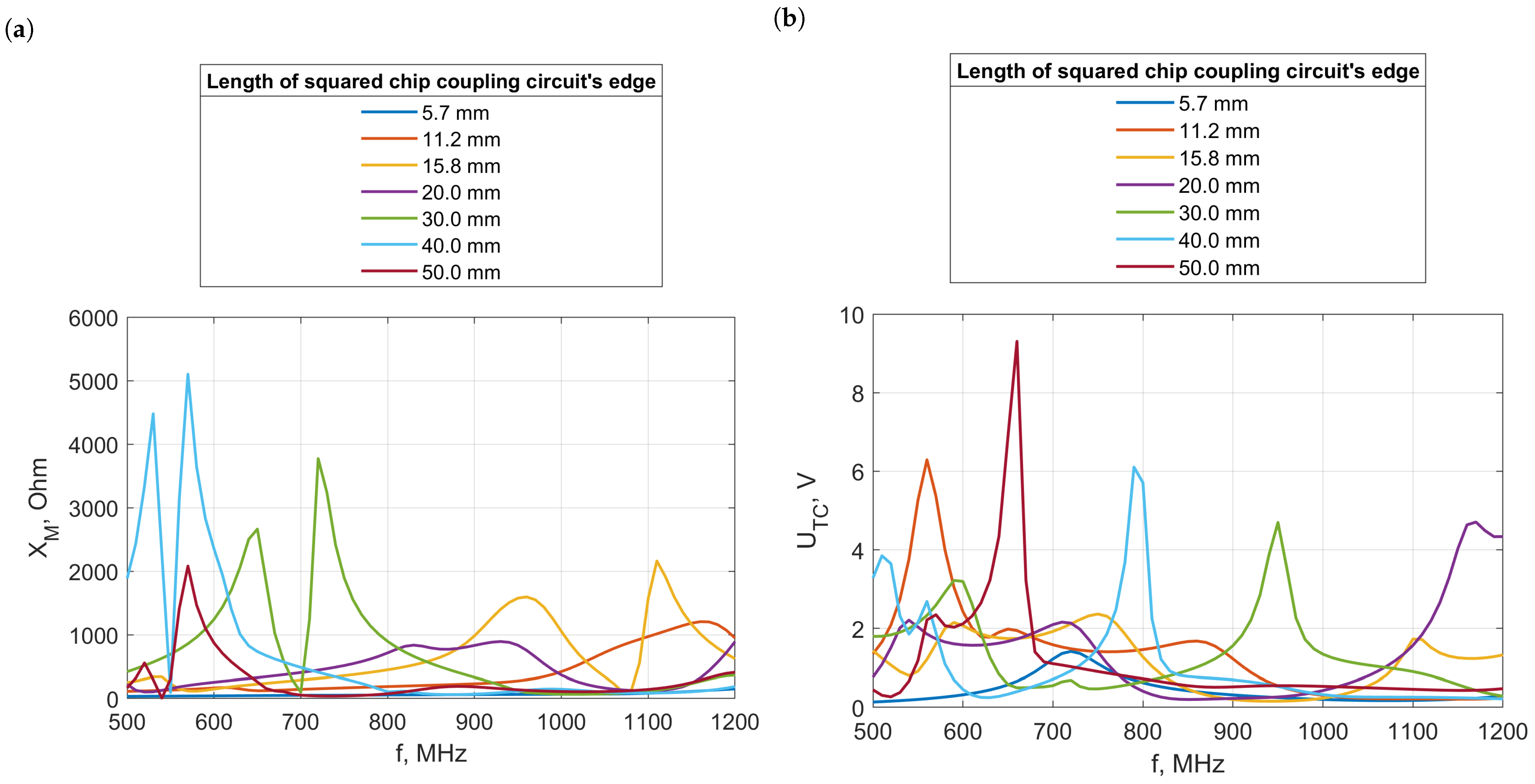
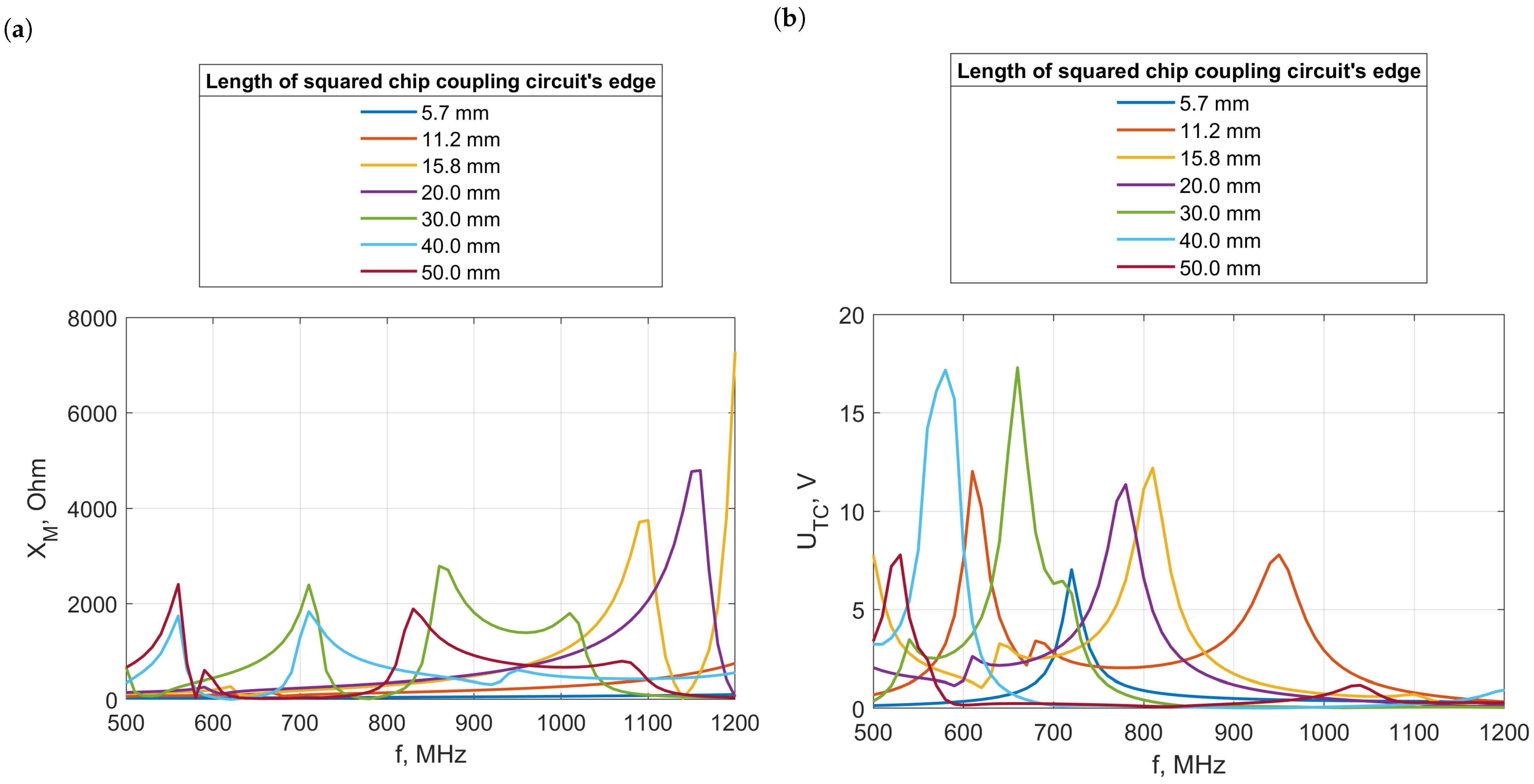
To evaluate these designs, square coupling circuits with varying side lengths were tested: 5.7 mm, 11.2 mm, 15.8 mm, 20 mm, 30 mm, 40 mm, and 50 mm. These dimensions were chosen to reflect common sizes of decorative and functional elements in clothing, ranging from small sequins to large buckles. Each antenna arm extends 8 cm from the edge of its coupling circuit. The calculated values of mutual inductance X M and chip voltage U TC for these configurations are illustrated in Figure 12, Figure 13 and Figure 14.
The alteration in the shape of the coupling circuits significantly impacted the relationship between the mutual inductance X M and frequency. With circular circuits, mutual inductance consistently increased with frequency. In contrast, square circuits displayed extrema in both mutual inductance and chip voltage U TC , with these extrema occurring at different frequencies for each chip coupling circuit. Notably, the first and third designs, which only differed in the angle between the antenna arms and the edges of the coupling circuit, exhibited similar distributions of extrema on the frequency axis. Across all designs, significantly higher chip voltages were achieved, suggesting that these transponders could potentially offer a greater read range compared to those using the traditional two-loop chip coupling circuit. Notably, the highest voltages were recorded in the designs featuring U-shaped antenna arms.

3.1.4. Transponders without Antenna Coupling Circuit

Since the radiator itself generates a magnetic field, this raises the question of whether this field alone is sufficient for the inductive coupling of the embroidered antenna with the chip. It is evident that transponders designed this way tend to have weaker inductive coupling compared to designs with a dedicated antenna coupling circuit. However, eliminating the coupling circuit reduces the consumption of conductive threads and lowers the antenna module resistance R A , which impacts the mutual inductance X M and chip voltage U T C , according to Equations (5) and (6).
It is important to recognize that there is an optimal value of mutual inductance at which the chip voltage peaks. In cases where the large dimensions of the chip coupling circuit result in an excessively high X M , reducing the size of the circuit could decrease X M to more desirable levels. The selection of the chip coupling circuit’s size and geometry should be tailored to the specific garment element on which it will be placed. Additionally, fabricating the antenna without a coupling circuit is simpler, uses less conductive thread, and requires less space on the garment, enhancing the versatility of this transponder design for various clothing applications.
A simple dipole antenna can be easily embroidered, even by beginners in sewing, opening up the possibility for the widespread adoption of such textile transponders among electronics and IoT enthusiasts. They could integrate these transponders into their systems and wearable devices. Transponders could be marketed as kits, consisting of a pre-assembled microelectronic module and conductive thread. Users’ tasks would be to embroider the dipole antenna and attach the microelectronic module as per the included instructions.
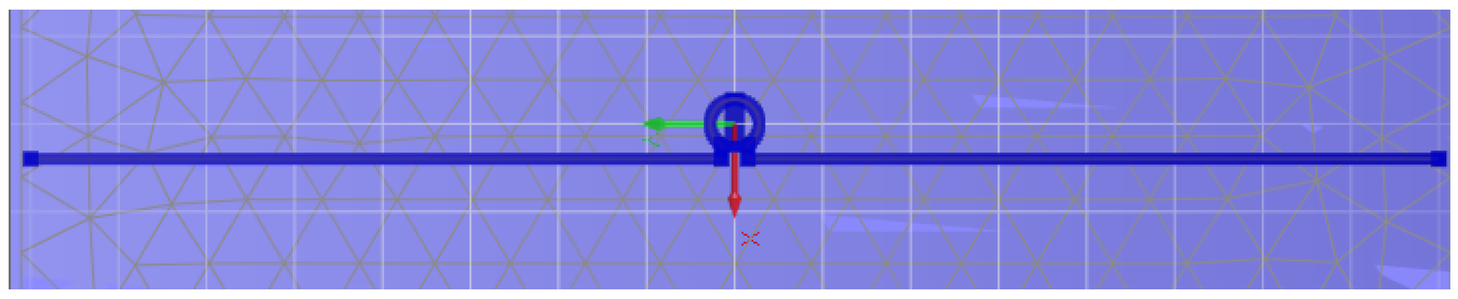
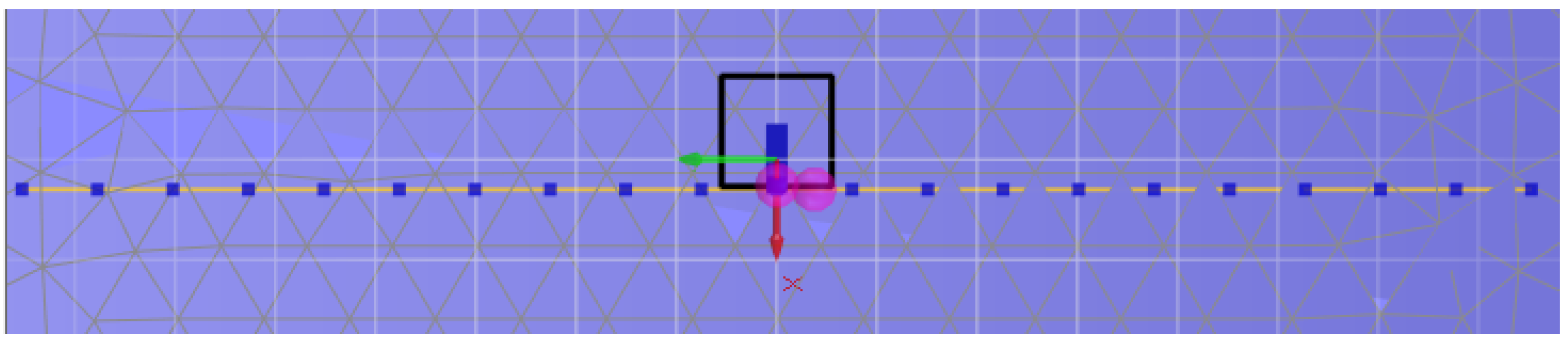
It should also be noted that placing the antenna directly in the middle of the chip coupling circuit results in the weakest coupling due to the opposing directions of the magnetic induction vectors on either side of the conductor. Positioning it outside the chip’s area leads to the strongest coupling.
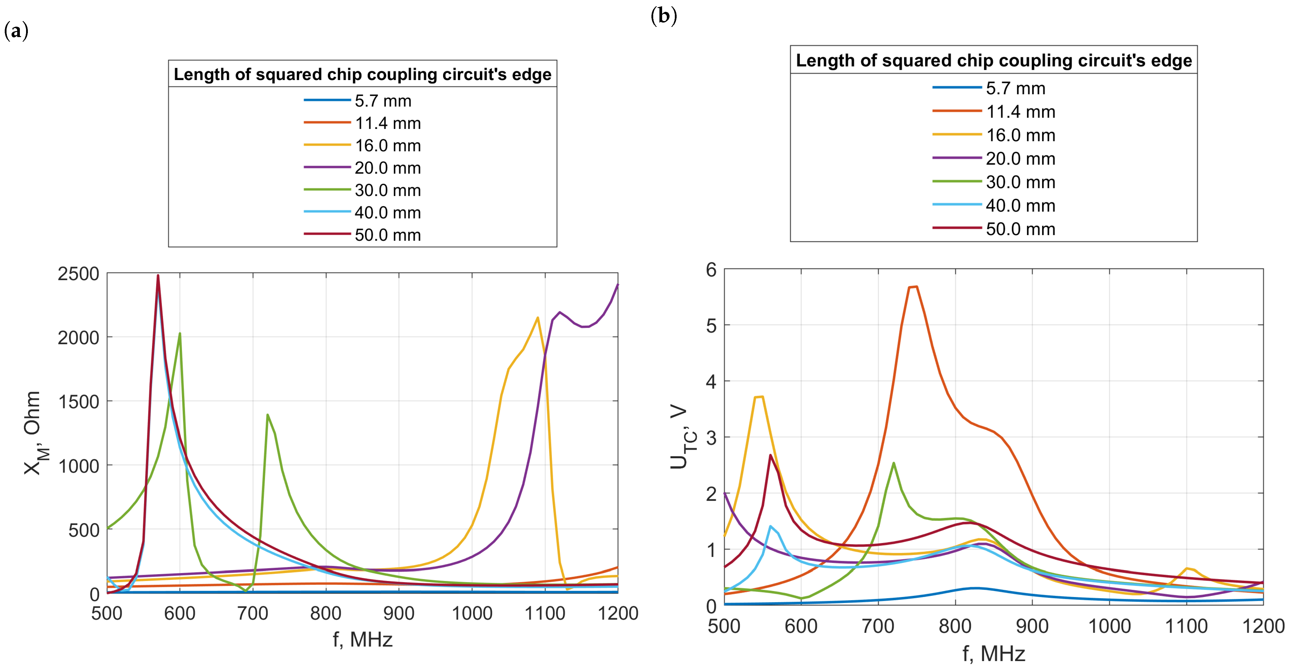
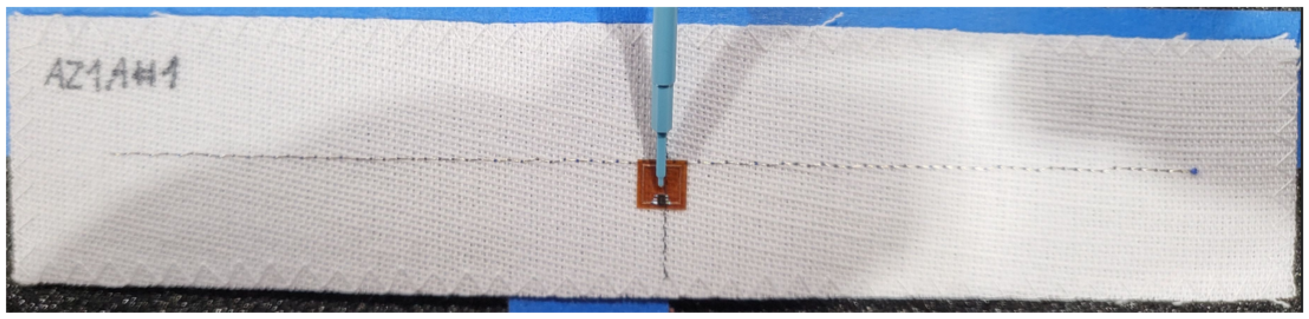
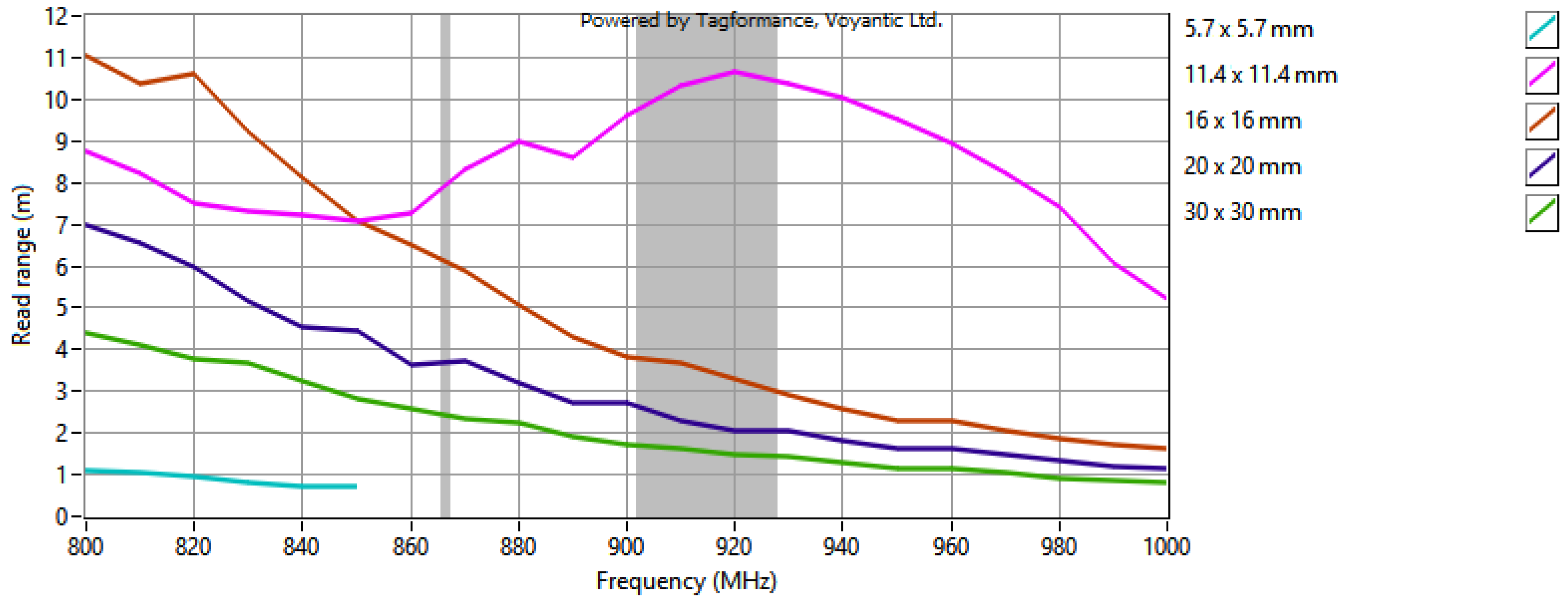
A simulation was conducted using a dipole antenna with a length of 16 cm, with the microelectronic circuit positioned at the antenna’s midpoint. The antenna was placed as close to the edge of the chip coupling circuit as possible while remaining outside its area, as depicted in Figure 15. Initially, square-shaped chip coupling circuits with side lengths of 5.7 mm, 11.4 mm, 16 mm, 20 mm, 30 mm, 40 mm, and 50 mm were examined. The values of the mutual inductance X M and chip voltage U TC were calculated for each model (Figure 16). These results can be compared to those shown in Figure 12, where the primary difference is the absence of the antenna coupling circuit in the current models. As anticipated, the voltage values obtained in this configuration were lower. Notably, two frequency ranges were observed in this setup, each corresponding to a maximum voltage for the circuit. The highest voltage in this setup was achieved with the 11.4 mm, square, while larger squares performed better in the previous configuration with an antenna coupling circuit.
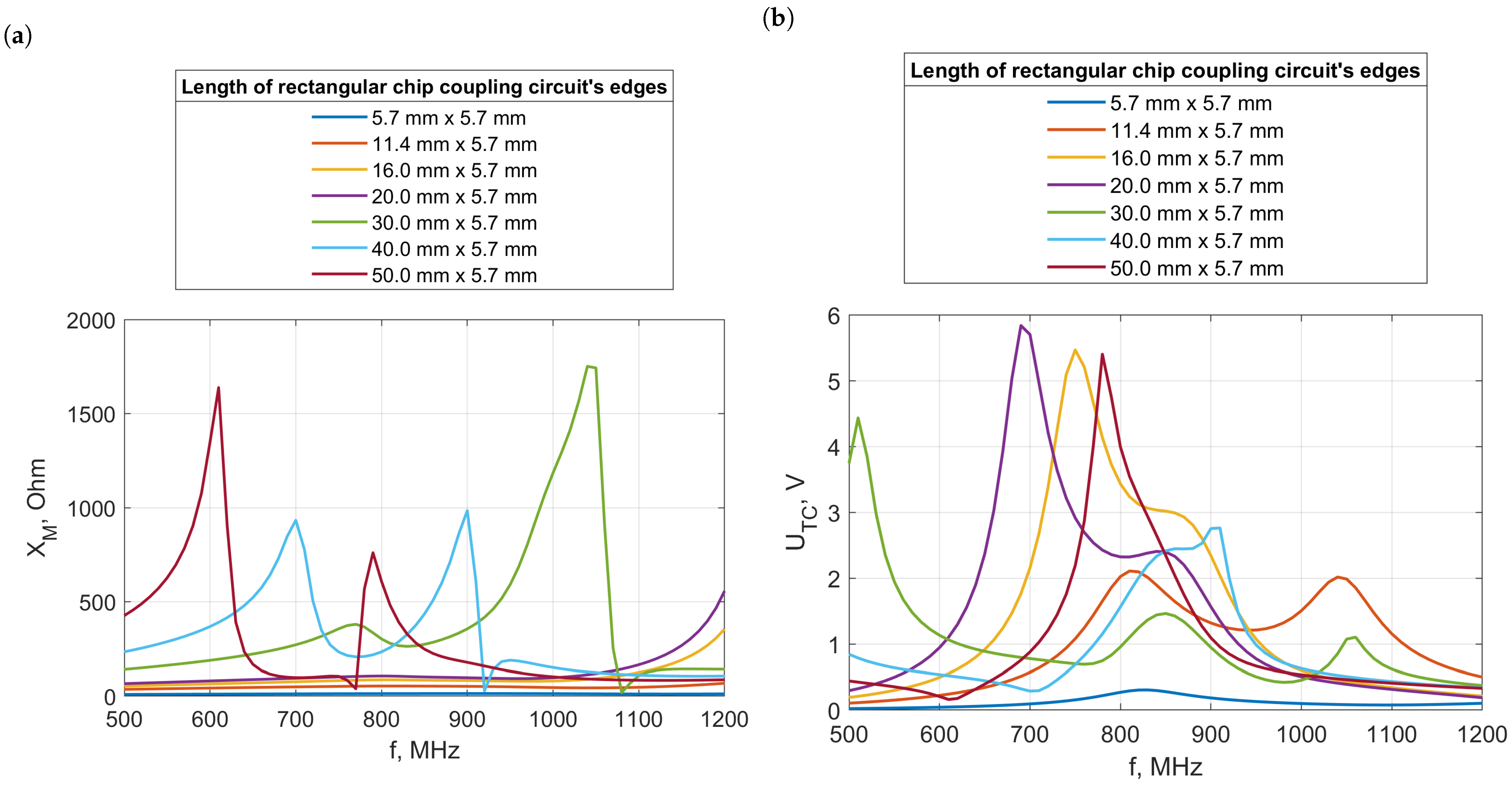
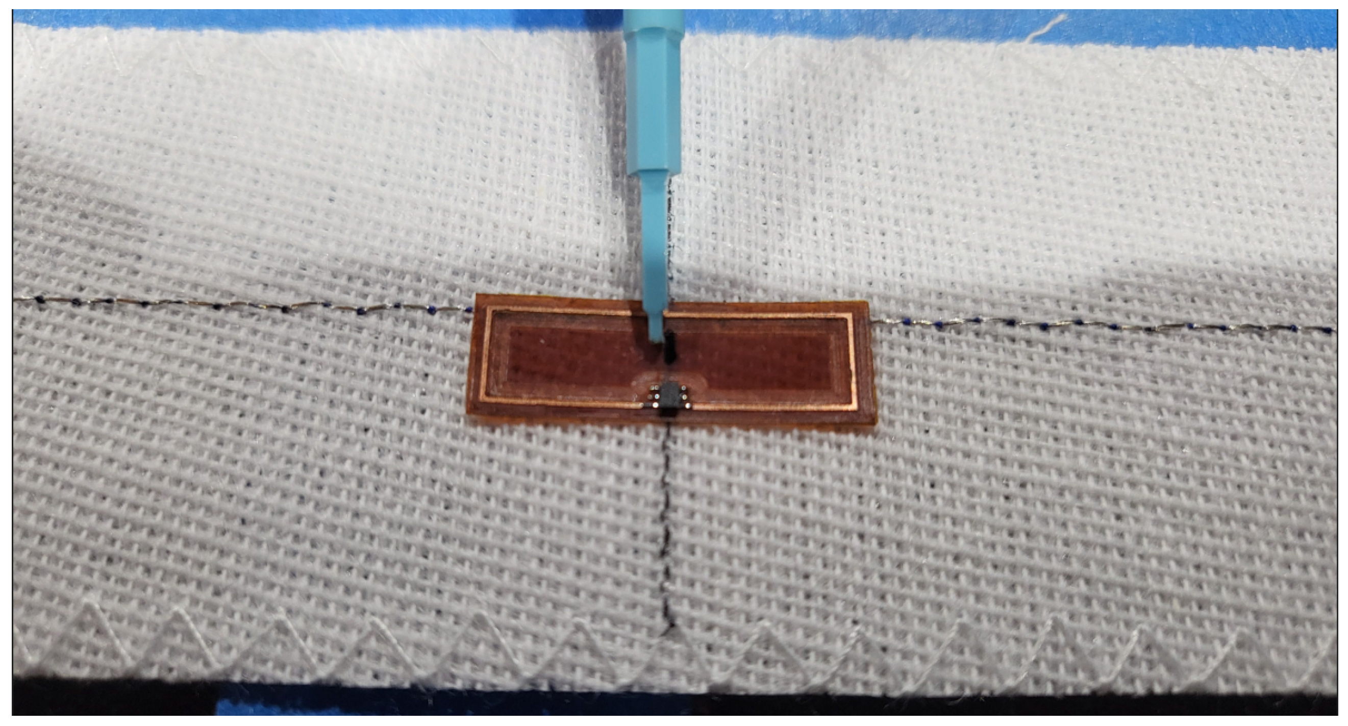
The magnetic flux density decreases with increasing distance from the conductor. To maximize it, it is advantageous to position the largest possible surface area of the coupling device as close to the antenna as possible. Consequently, rectangular coupling circuits were designed (Figure 17). Each chip coupling circuit was shaped as a rectangle with a shorter side measuring 5.7 mm, while the length of the longer side varied among 11.4 mm, 16 mm, 20 mm, 30 mm, 40 mm, and 50 mm.
Initial calculations were conducted for configurations where the coupling circuit’s longer side was adjacent to the antenna (Figure 18). By shortening one side and extending the other side closest to the conductor, an increase in chip voltage was observed across almost all modules. Furthermore, the frequency at which the maximum chip voltage was reached remained consistent across most configurations.
For clothing designers, rotating the rectangular microelectronic layout so that its shorter edge is parallel to the antenna may seem beneficial (Figure 19). However, this configuration results in a reduction in the magnetic flux enclosed by the circuit, as the surface area close to the conductor generating magnetic induction is shifted to a region farther from the antenna. This effect is evident in the observed decreases in the mutual inductance X M and U TC , as illustrated in Figure 20. As expected, these voltages are lower compared to those obtained from transponders with a square antenna coupling circuit.
Nevertheless, transponders without a square coupling circuit demonstrated greater stability in positioning the maximum chip voltage on the frequency axis. This indicates a significant influence of the antenna coupling circuit’s length on this parameter, highlighting a critical design consideration for optimizing transponder performance.

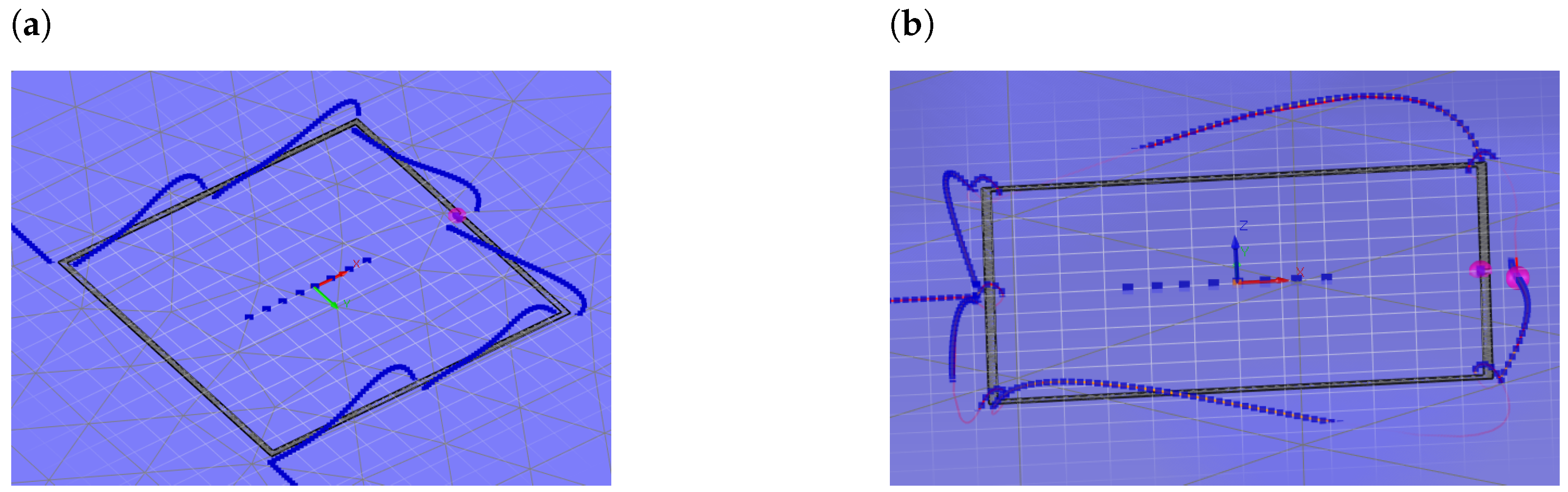
3.1.5. Transponders with Antenna Coupling Circuit Wrapping around Chip Coupling Circuit

Wrapping the conductive thread around the chip’s coupling circuit can create a transponder design that minimizes the likelihood of the coupling systems separating and, consequently, deteriorating the read range. However, the geometry of the weave must be carefully designed in accordance with the laws of electromagnetism to ensure adequate inductive coupling between the circuits.
When sewing the microelectronic circuit, the formation of knots occurs where the conductive thread crosses the path of the chip coupling circuit perpendicularly. According to Equation (8), if the thread at the knot wraps around the coupling system’s path at a right angle, the magnetic flux at that point will be zero. However, if the knots are sufficiently spaced, the thread segments between them will run parallel to the microelectronic circuit’s path. These straight segments are crucial as they generate the magnetic field that enables inductive coupling between the antenna and the chip.
For effective inductive coupling, it is essential to sew the conductive thread in a manner that, despite the necessary knots, emulates the shape of a planar antenna coupling circuit. While ignoring the knots, the magnetic flux density is described by Equations (12) and (13). Nevertheless, the presence of knots and the curvature of the thread between them significantly impacts these parameters, influencing the overall effectiveness of the coupling.
Designers may opt to sew the coupling circuit with only one or a few closely placed knots for aesthetic reasons, as discussed in the section on transponders without an antenna coupling circuit. In such cases, it is crucial to carefully position the microelectronic circuit relative to the radiator. Reference [46] presented designs where the conductive thread wrapped around the chip coupling circuit effectively serves as the antenna coupling circuit and generates a magnetic field strong enough to compete with the radiator.
Additionally, there are several technical limitations to consider. The use of insulated conductive thread is necessary to prevent short circuits, and unlike previous planar designs, it is not feasible to substitute this thread with conductive inks. The microelectronic module’s manufacture is also more complex, requiring an opening in the middle of the chip circuits, and the chip housing must be designed so as not to obstruct the thread placement.
This construction method is also suitable for clothing elements that extend beyond the fabric, where the conductive thread encircles the chip coupling circuit without passing through the material. In such designs, special attention must be given to ensure that the thread does not slip and that the geometry of the coupling circuit remains intact.
As discussed in this section, simulations were performed on transponders featuring square-shaped chip coupling circuits with a side length of 11.4 mm. This particular module size was selected based on the high chip voltage achieved in previous designs, suggesting its efficacy. One of the goals of this construction was to address the issue of separation between the antenna and chip coupling circuits. To ensure a robust connection, careful consideration was given to the number and placement of knots. It was determined that securing the chip circuit at its corners, or, additionally, at the midpoints of its sides, would be sufficient.
It is important to clarify that the primary purpose of sewing the microelectronic circuit with conductive thread is not just to attach it to the material, but more crucially, to prevent the coupling circuits from moving relative to each other. For additional security, regular threads can be used for further fastening.
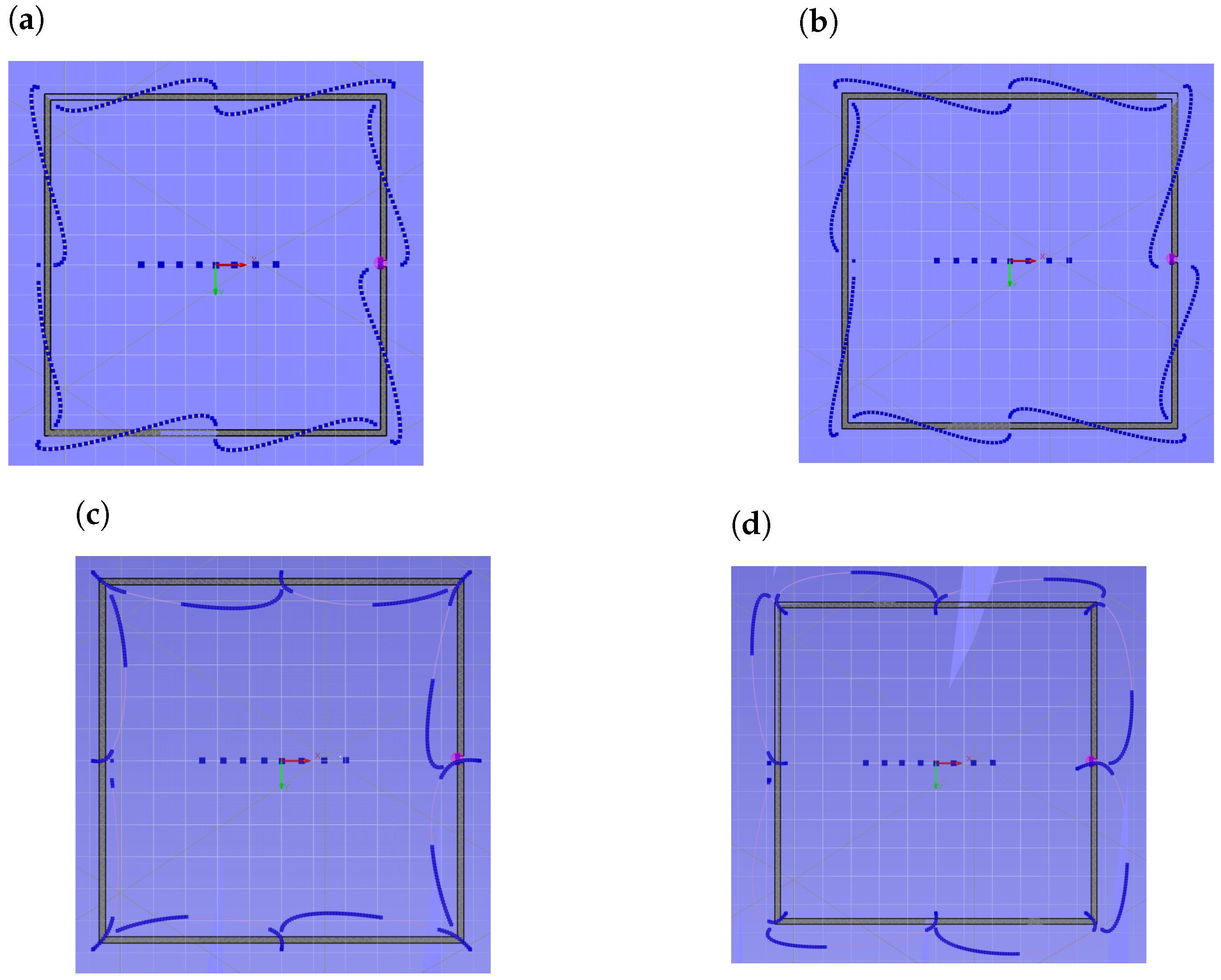
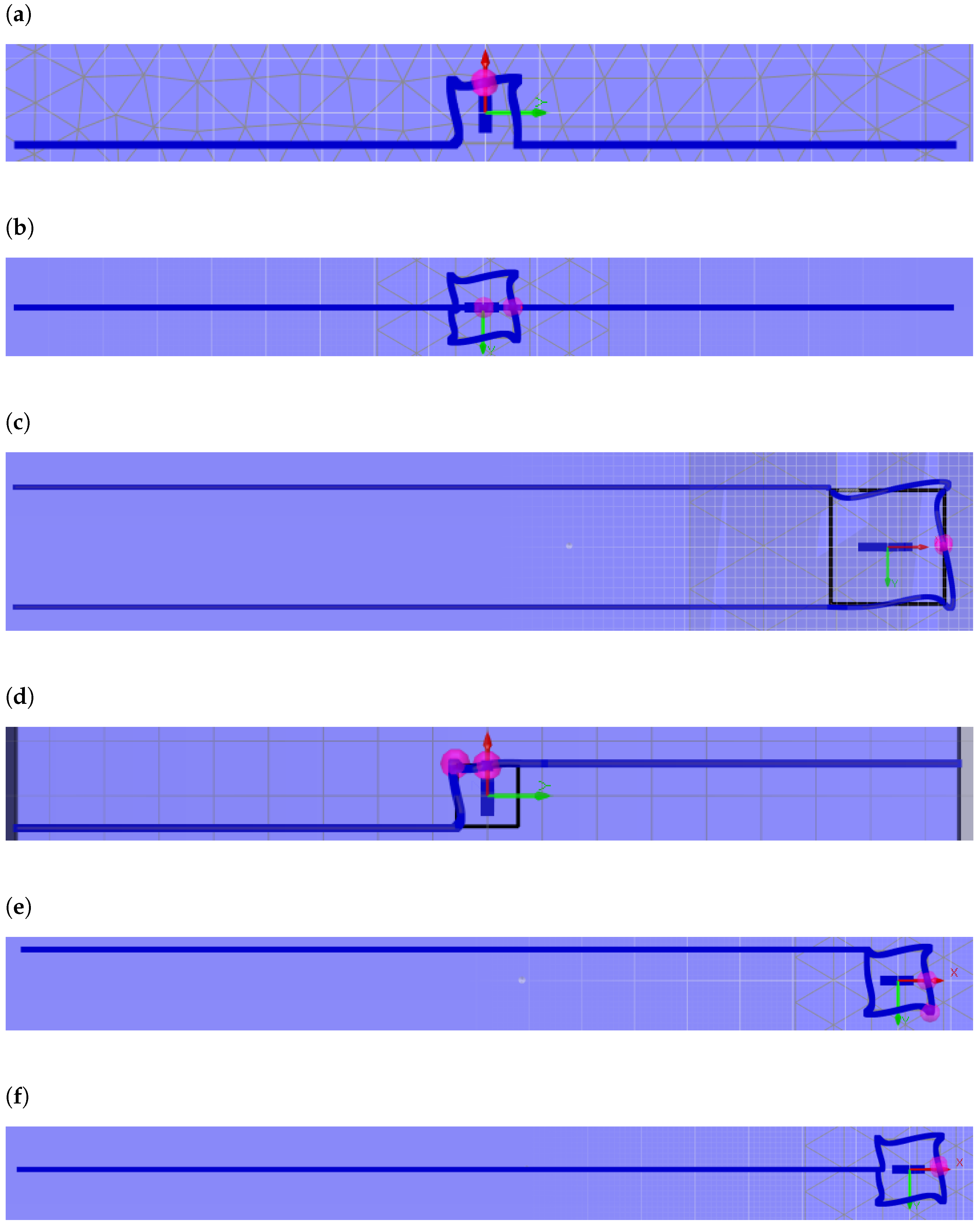
Initially, modules with knots placed at the corners and midpoints of the sides were tested to assess how the number of knots affects inductive coupling. Four wrapping methods proposed to optimize this effect are illustrated in Figure 21. In the first method, shown in Figure 21a, the knot starts on one side of the chip coupling circuit’s path and ends on the other, positioning the thread diagonally across the path. Another approach, depicted in Figure 21b, explores changing the winding direction of the thread.
For segments between knots, a parallel alignment with the circuit’s path was tested. The knots can be initiated and concluded on the same side of the path, which can be either inside or outside the chip coupling circuit’s area. The choice of side determines whether the area of the antenna coupling circuit is larger or smaller than that of the chip circuit, influencing the potential for inductive coupling. It is anticipated that configurations with parallel segments and a larger circuit area will exhibit higher values of mutual inductance X M . However, variations in the amount of conductive thread used for each design also impact the resistance R A as indicated by Equations (5) and (6), affecting the resultant X M and chip voltage U TC .
For each of the four wrapping methods, a transponder model was constructed to match the design featuring a planar square-shaped coupling circuit, as shown in Figure 11a. The model with the wound antenna coupling circuit is depicted in 
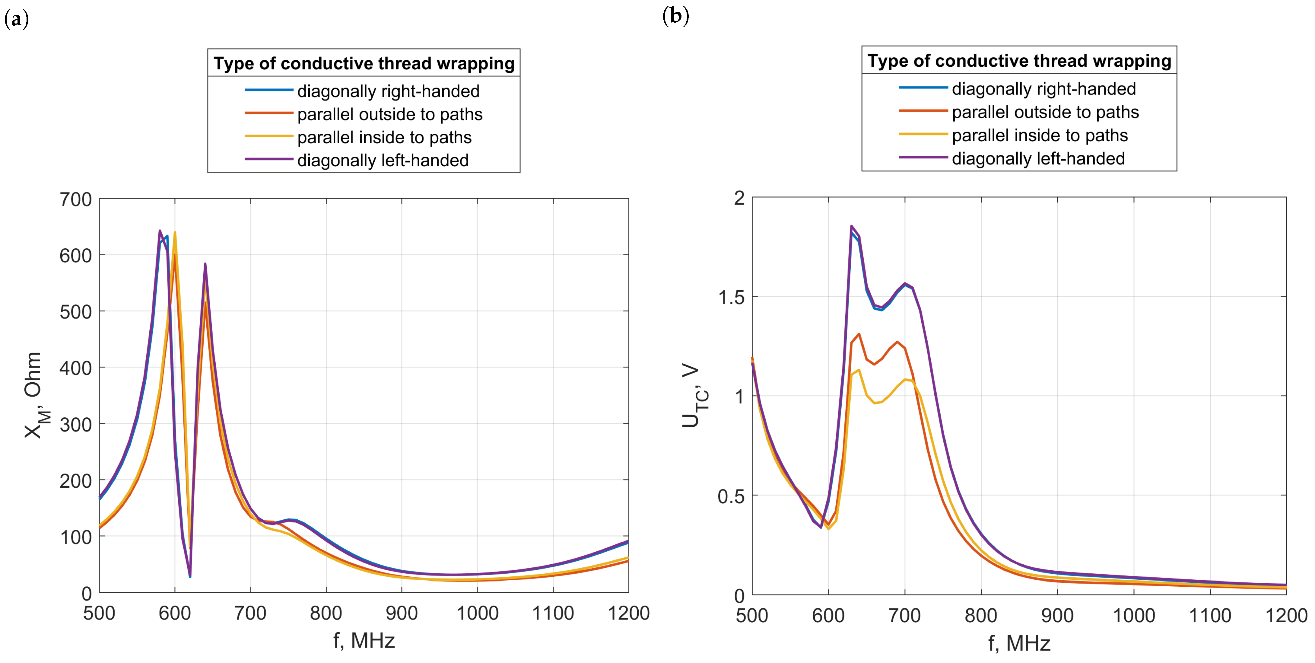
Figure 22. The length of the conducting thread used to construct the antenna and its coupling circuit varied depending on the wrapping method, measuring 203.97 mm for methods 1 and 2, 215.079 mm for method 3, and 207.08 mm for method 4. The antenna arms for each model were consistently 160 mm in length. The results of mutual inductance X M and chip voltage U TC from these models are presented in Figure 23.
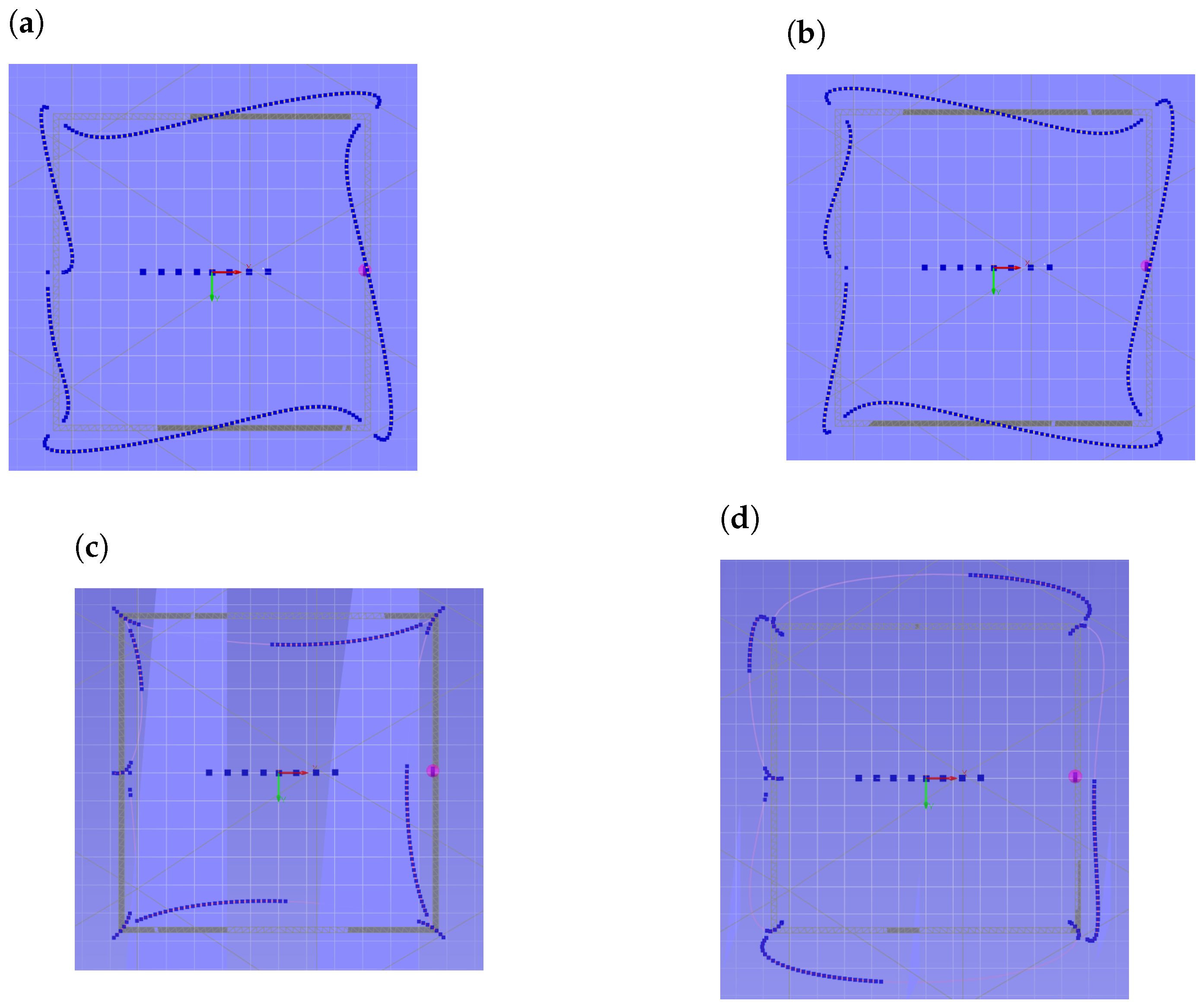
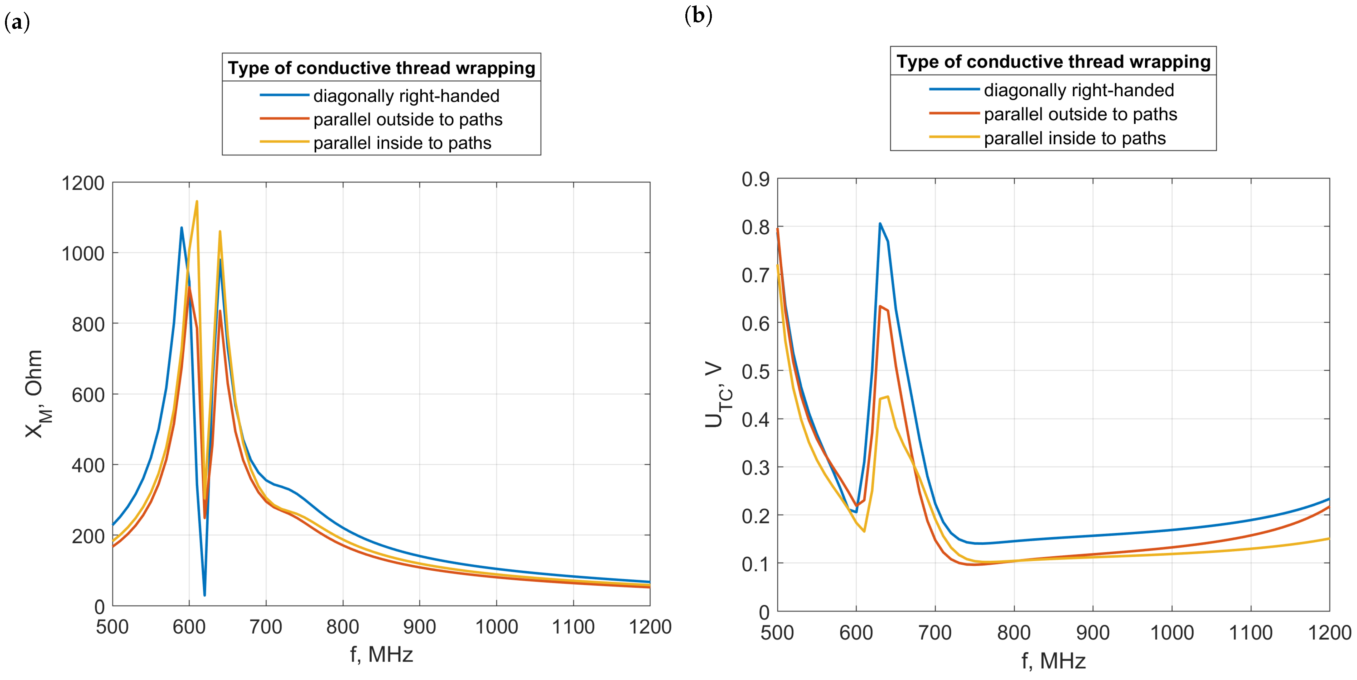
The same four winding methods previously described were applied to wind the coupling circuit with conducting thread, but only at the corners, as illustrated in Figure 24. Additionally, for the method involving sewing with knots at the corners, six different antenna geometries were examined (Figure 25). This approach was intended to mirror the pattern of constructions with a planar antenna coupling circuit. Consequently, transponders with identical arm arrangements, similar to those depicted in Figure 11a–c, were tested.
Three additional geometries were also proposed to accommodate specific design needs. In these configurations, the coupling circuit is positioned not in the middle, but at the end of the antenna, or only two sides of the chip coupling circuit are wound. These designs are particularly suitable for transponders that are integrated into clothing elements which protrude beyond the material, allowing for greater design flexibility and application-specific customization.
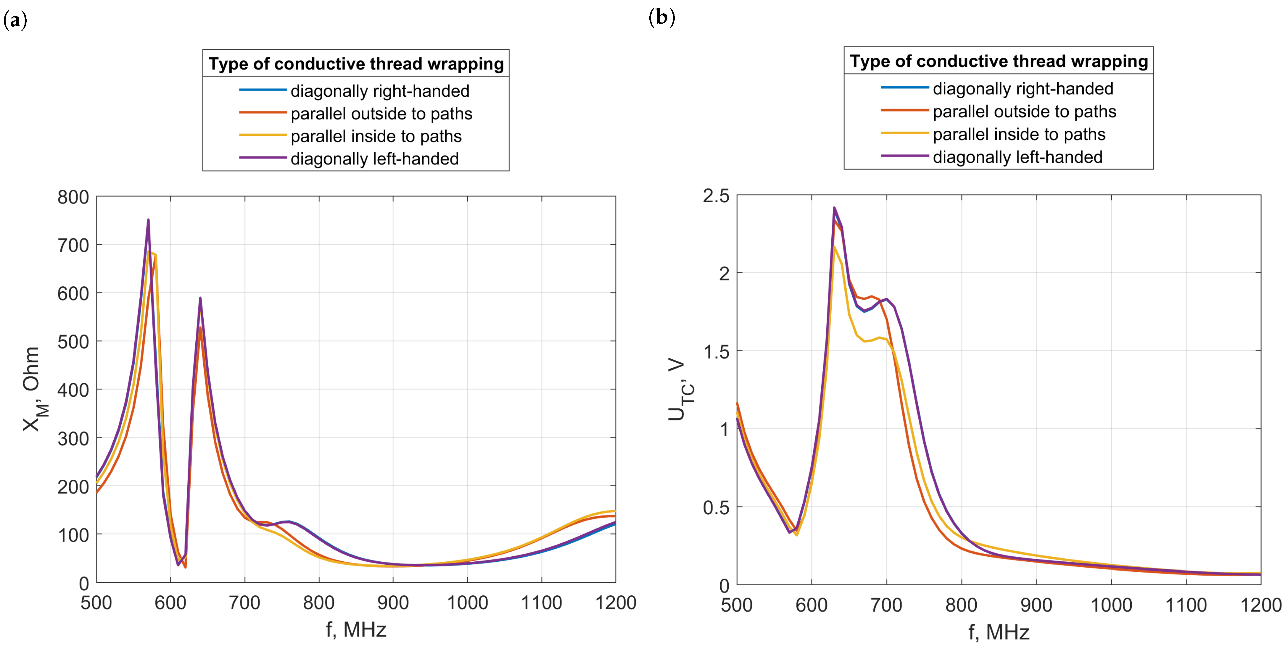
The results from the first construction, depicted in Figure 26, allow for a comparison of the effects of using different numbers of nodes in the winding. This particular coupling circuit required less conducting thread, with lengths measuring 200.10 mm for the first two cases, 206.52 mm for the third, and 199.68 mm for the fourth. Notably, the second and third weaving patterns, between 0.6 and 0.7 GHz achieved higher mutual inductance X M values compared to configurations with a greater number of nodes. This observation correlates with a significant decrease in voltage for these models, suggesting that lower X M values are closer to being optimal for strong coupling in this context.
Interestingly, the weave with the weakest coupling exhibited the highest chip voltage U TC . This phenomenon indicates that a greater number of nodes, which typically weaken the magnetic field, can lead to higher voltages. In scenarios where the magnetic field is overly strong, it can be moderated by adding more nodes. Conversely, reducing the number of nodes can strengthen a weak magnetic field. The variations in X M and U TC due to different node counts also stem from changes in antenna resistance, which, according to Equations (5) and (6), affect these values both directly and indirectly through alterations in X M . Additionally, designs that require a larger number of nodes—and consequently more conducting thread—tend to have higher resistance.
Given the minimal differences in the X M and U TC values between models with different winding directions of the thread, subsequent simulations focused solely on the right-hand winding case.
The results from the subsequent two constructions, as depicted in Figure 27 and Figure 28, reveal a clear dependency on the type of wrapping used. In the frequency range of 0.6 to 0.7 GHz, where the maximum chip voltage U TC occurs, the X M graph indicates an optimal value that lies between those for the individual windings. Notably, neither the braid with the strongest nor the weakest coupling produced the highest U TC . Instead, the highest voltage was achieved by the model featuring the diagonal pattern. Conversely, for constructions with a U-shaped antenna, the weakest coupling corresponded to the highest chip voltage.
In this scenario, reducing the size of the coupling circuit could decrease the magnetic flux, making the transponder more suitable for smaller clothing items. Additionally, having the antenna arms directed in one direction also conserves space, facilitating the application of the transponder. Although the differences in chip voltage among the wrapping methods are smaller compared to the design where the antenna passes through the center of the coupling circuit, a noticeable shift in their maximum values along the frequency axis is observed.
Compared to designs where arms are perpendicular to the coupling circuit, significantly higher chip voltages were recorded in these models. The examination of the corresponding X M values, which were notably lower, suggests that designs with perpendicular arms may exhibit excessive coupling. This observation implies the need for a coupling circuit with a reduced surface area. Moreover, when compared to models with planar coupling circuits, this model with a coupling circuit chip of equivalent size achieves higher or lower chip voltages, depending on the effectiveness of the selected wrapping method.
In Figure 29, Figure 30 and Figure 31, results are presented for constructions designed specifically for clothing elements where the conductive thread wraps around without passing through the fabric. The shapes of the plots in Figure 29 resemble those seen in Figure 26, with the main difference being the removal of one side of the antenna coupling circuit. This modification led to a higher level of inductive coupling, which, interestingly, resulted in a reduction in the chip voltage U TC . This outcome likely stems from the specific arrangement of the antenna arms.
The two subsequent designs, shown in Figure 30 and Figure 31, differ only in the placement of the coupling circuit relative to the radiator. The plots from these configurations were similar, yet for the coupling circuit positioned at the midpoint of the radiator, higher voltages were recorded. This increase can be explained by how the surface of the circuit covers the magnetic flux density vectors, which vary in direction relative to the radiator’s orientation. As a result, this strategic positioning helps mitigate the excessive coupling that typically leads to low U TC values in these designs.
In most of the designs examined, the highest chip voltage U TC values were achieved with the diagonal pattern, which provided the lowest mutual inductance X M values. This result is due to the surface area of the square-shaped chip coupling circuit, measuring 11.4 mm per side, which generated a substantial magnetic flux, often exceeding the optimal threshold. Consequently, such transponders are advantageous when a small-sized coupling circuit is needed. Additionally, considering the other two weave patterns becomes important when aiming to increase the X M value, should it fall below the optimal range. The positioning of the antenna arms plays a critical role in influencing the resultant values of X M and U TC .
Interestingly, unlike previous transponder groups, each weave pattern in this set peaked at the same frequency, except for the U-shaped antenna. Generally, for various arm arrangements, the peak values occurred within the 0.6 to 0.7 GHz range, though they varied in shape and potentially extended beyond this frequency span. This finding highlights the significant impact of weave geometry and the length of the antenna coupling circuit on the performance of the transponders, despite the consistent dimensions of the chip coupling circuit.

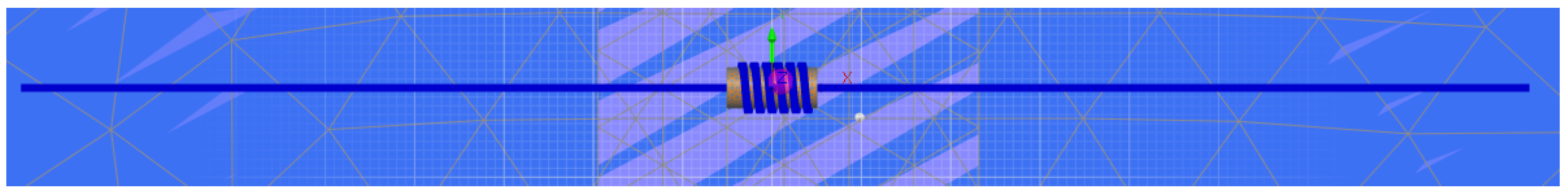
3.1.6. Transponders with Chip and Antenna Coupling Circuits Positioned on the Core

In this transponder design, the conductive wire is wound around a core to form coils, creating an antenna coupling circuit in a solenoid configuration. Employing multiple turns can significantly enhance the magnetic flux, even in smaller coupling systems. For the simulation, a single-loop coupling circuit with a diameter of 5.7 mm was used, resulting in lower mutual inductance X M and chip voltage U TC values, as illustrated in Figure 10. The coils themselves had a diameter of 4.9 mm, which is slightly smaller than that of the chip coupling system, allowing the chip to be placed directly atop the coils. The spacing between the coil turns was set at 1.33 mm.
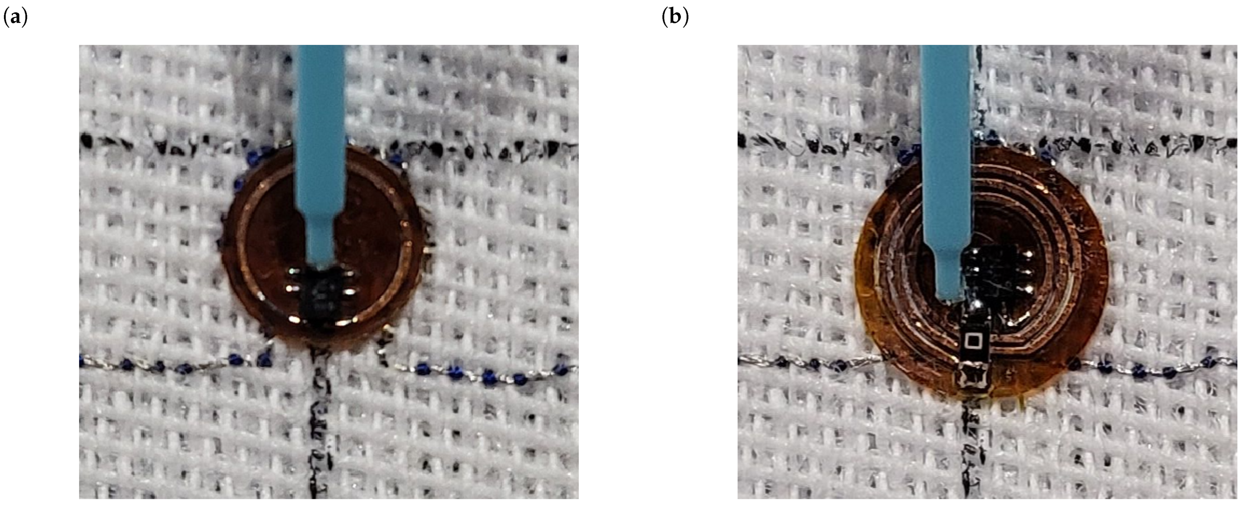
The core of the coils measured 4.5 mm in diameter and 8 mm in length (Figure 32). It was made from ’Glass, Bead’, a material chosen from the EMCoS Studio library that resembles the type of glass commonly used in ornaments and jewelry. This choice not only enhances the transponder’s decorative appeal, but also aligns with the dimensions of typical decorative beads, making the design aesthetically pleasing for applications where appearance is crucial. Additionally, functional elements such as cylindrical buttons, frequently found on garments like trousers or denim jackets, could serve as practical alternatives for the core material, further integrating the transponder seamlessly into fashion items.
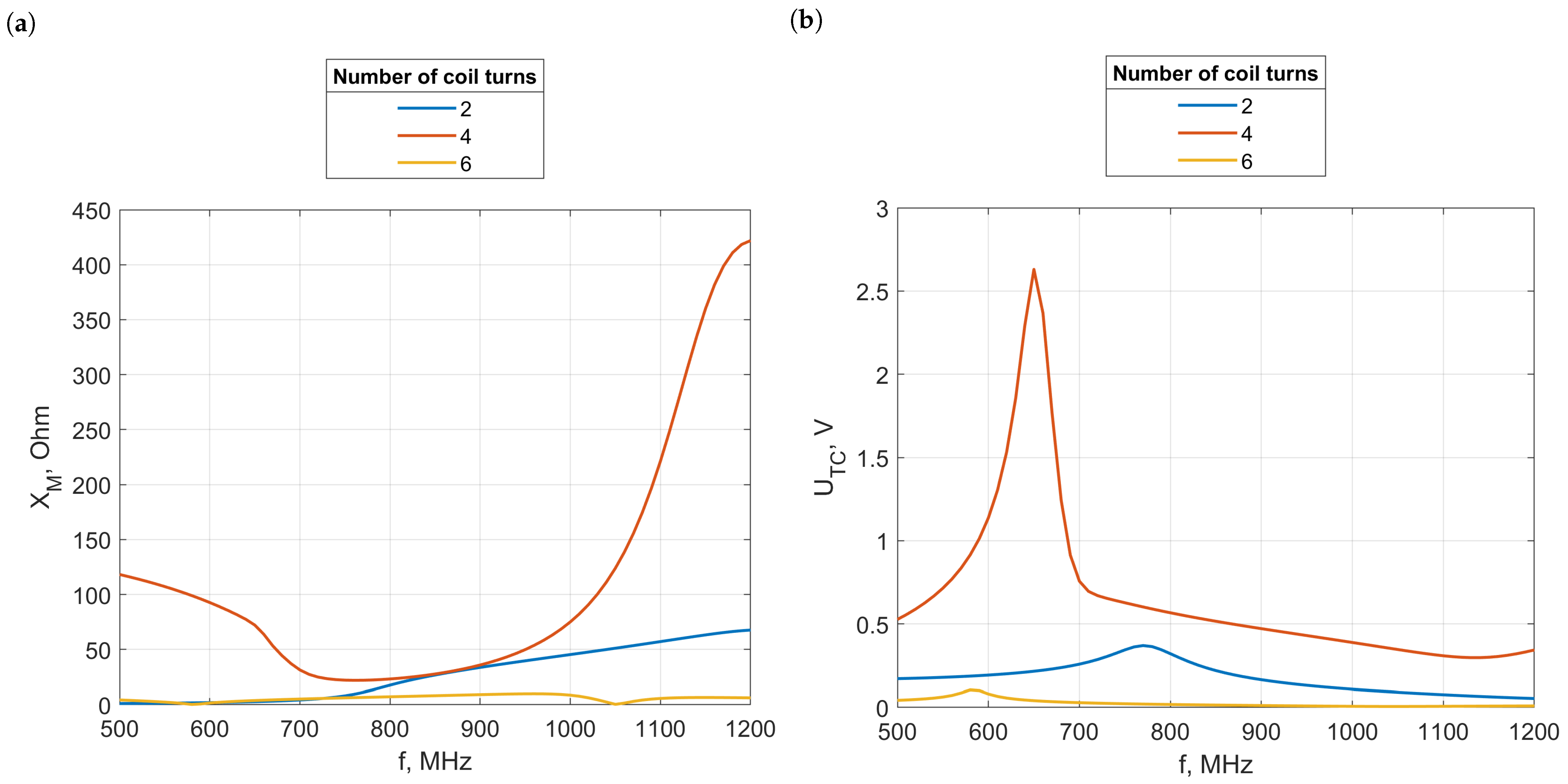
Three transponder models were developed, each incorporating a different number of turns in the antenna coupling circuit: two, four, and six turns, respectively, as shown in (Figure 33). The impact of the number of turns on the mutual inductance X M and chip voltage U TC is detailed in Figure 34. Among these, the model with four turns demonstrated a notable enhancement in inductive coupling compared to those with a planar coupling circuit. Although its maximum U TC was close to the configurations with two and three loops, it did not surpass them.
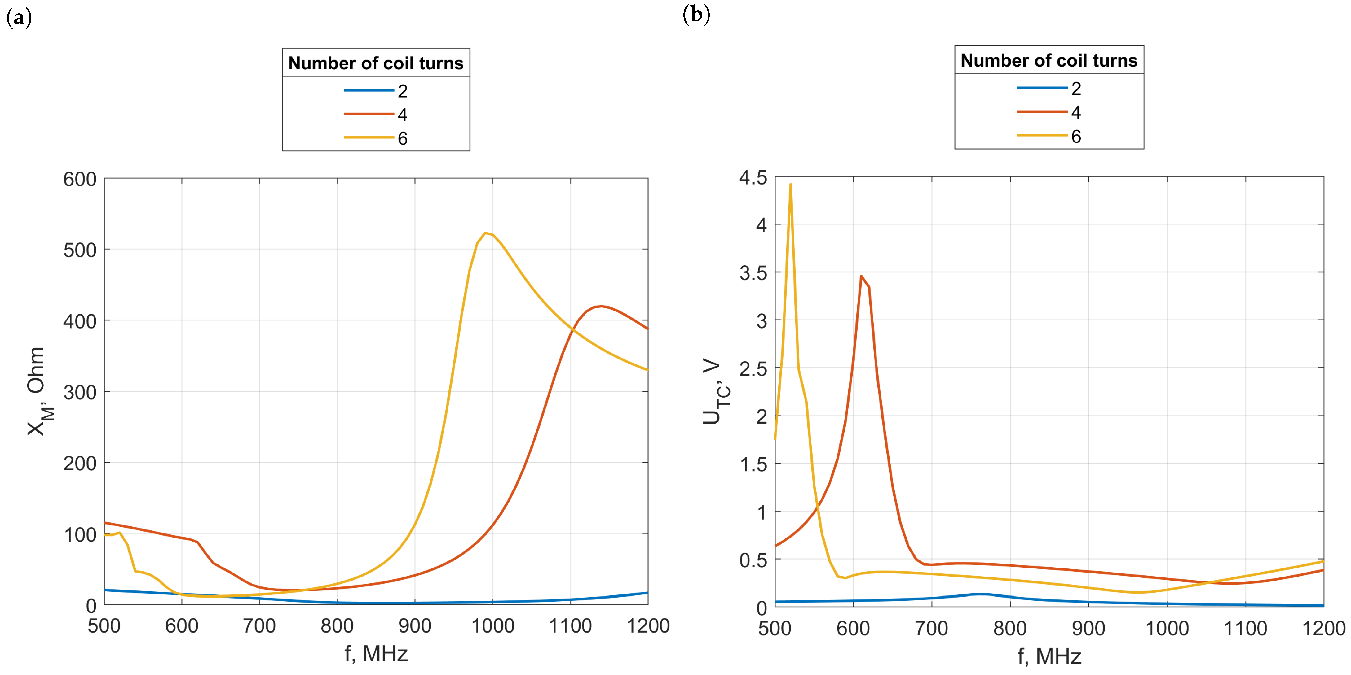
In refining this model, the initial step involved winding conducting thread onto the core, followed by positioning the microelectronic module onto the coils. Considering that the magnetic field is confined within the solenoid, it is crucial to calculate the magnetic flux across the chip coupling circuit’s cross-section to ensure that it is fully enveloped by the magnetic field. To achieve this, a new model was devised where coils were wound around both the core and the microelectronic module. All model parameters were kept constant, except for the coil diameter, which was increased to 6.3 mm to cover more surface area. This adjustment resulted in a slight increase in voltage across all numbers of turns (Figure 35). Moreover, there was a noticeable shift in the frequency maximum, likely due to the larger coil diameter and the resulting increase in the length of the entire antenna module.
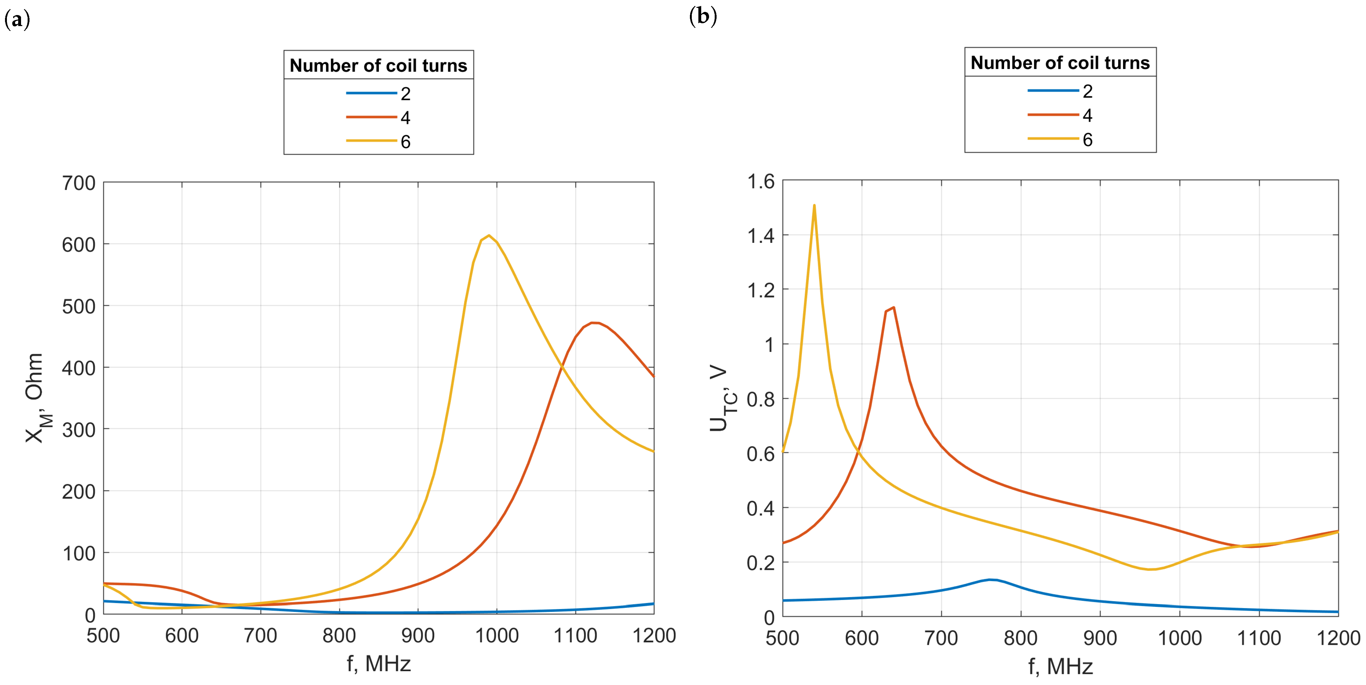
In both initial models, the configuration with six turns underperformed, which was likely due to the excessive distance between each turn. To remedy this, the spacing between the turns was decreased to 0.8 mm in a subsequent iteration of the model. This change was implemented in the transponder design where the microelectronic module is mounted directly on the antenna system. As shown in Figure 36, this adjustment met expectations: the revised model with six turns now achieved the highest chip voltage U TC .
Furthermore, reducing the distance between the turns not only improved the performance of the model with six turns but also had a positive impact on the four-turn model, resulting in an increased chip voltage. Conversely, this modification led to a decrease in voltage for the model with two turns. This outcome suggests that the optimal spacing between turns can vary significantly depending on the total number of turns in the antenna coupling circuit.
In the final phase of this research, a pivotal modification was made to the initially simulated model by changing the core material. Instead of the material commonly found in the clothing industry, ferrite, a popular core material in electronics, was selected. The specific type of ferrite chosen from the EMCoS Studio library is labeled “N30”. As depicted in Figure 37, the resulting chip voltage U TC was lower than that obtained with the glass core. It exhibited a noteworthy characteristic: the slopes of the voltage maxima decreased more gradually, thereby covering larger frequency ranges. This alteration in core material also notably enhanced the performance of the model with six turns, which had previously shown suboptimal results.

3.2. Experimental Research

The selected designs of transponders from the first two described groups were fabricated to measure their operating ranges. All read range measurements were conducted in an anechoic chamber. Initially, the impact of the number of loops on the circular coupling circuit of the chip was investigated. For this purpose, an antenna with a coupling circuit in the form of a 5.7 mm diameter loop, sewn with Agsis thread, was utilized. Two new microelectronic setups were fabricated: one with a single loop and the other with three loops (Figure 38). It is worth noting that the circuit with two loops had already been prepared and used in previous studies. Each of these circuits featured a diameter with the largest loop equal to 5.7 mm and with a path width of 0.2 mm. Additionally, there was a gap between the loops, which was equivalent to the path width.
For each of these chip coupling circuits, the read range was measured (Figure 39). The wideband UHF reference Tag v1 delivered with the Voyantic system was utilized to set up the measurements. The parameters of the Voyantic sweep settings were configured as follows: a start frequency of 800 MHz and a stop frequency of 1000 MHz with a step of 10 MHz, a minimum power of −5 dBm, and a maximum power of 25 dBm with a step of 1 dB. The sweep direction was set to rising. The transmitter boasted an output power of 29 dBm, with its antenna offering a maximum gain of 6 dBi. The receiver’s sensitivity was calibrated to −70 dBm, and its antenna provided a gain of 6 dBi. The ISO 18000-6C communication protocol was applied with the query command, employing a forward link of 25 µs DSB-ASK and a return link of FM0, 40 kHz.
The measurement results indicate a significant difference in the performances of the transponders, with the dual-loop coupling system exhibiting a high read range, up to 9 m. But the obtained measurement results are consistent with the numerical calculations of the chip voltage for these transponders (Figure 10). In the case of one loop, the mutual inductance in such a transponder was noticeably lower, which should be attributed to its small size. Therefore, the read range was also low. The read range measurements were conducted over a narrower frequency range than the numerical calculations, which influenced the observed outcomes. Specifically, the range plot for the circuit with three loops shows a decreasing trend, with values that are lower than those for the circuit with two loops. However, this does not necessarily indicate a poorer performance of the three-loop circuit; rather, it suggests a shift of the maximum response toward lower frequencies compared to the numerical calculations. Given that the method for adjusting the maximum along the frequency axis has not yet been detailed, it is currently advisable to use the two-loop circuit. This configuration aligns more closely with the frequencies typically used in RFID systems, thus providing a more effective performance within the expected read range.
Microelectronic modules with square and rectangular chip coupling circuits were fabricated. It was decided to use them to construct a transponder with an antenna without a coupling circuit. A dipole antenna with a length of 16 cm was sewn with Agsis Syscom thread (Figure 40). Each module was placed in the center of the antenna so that the conducting thread was as close as possible to the edge of the chip coupling circuit. Next, the read range of the transponder was measured (Figure 41).
The obtained read range results were compared to the numerical calculations of the chip voltage for this transponder design (Figure 16). When comparing them, it was important to consider that the model used Litz wire, which has a resistance of 1.387 Ω /m, while Agsis Syscom wire has a higher resistance of 82 Ω /m. This results in a different value of the resistance of the embroidered antenna R A , which affected the obtained results. In both cases, the best result was achieved for the square with sides of 11.4 mm and 16 mm.
Rectangular configurations of the chip coupling were also fabricated. Using the same antenna as in the case of the measurements with square modules, transponders without the antenna coupling circuit were built (Figure 42), and their read ranges were measured (Figure 43).
The obtained measurements correspond to the calculated chip voltage presented in Figure 18. Both in experimental tests and numerical calculations, the best results were achieved by the module with a longer side equal to 16 mm. According to the calculations, modules with side lengths of 20 mm and 30 mm also allow for achieving a high read range. On the other hand, the module with a side length of 50 mm achieved a significantly worse read range in the measurements compared to what the calculated chip voltage would suggest. The reason for this could be attributed to the use of threads with lower conductivity for sewing the antenna, which, according to the formulas, led to an increase in the reactance X M . The higher value of X M , in turn, led to a decrease in voltage U TC compared to the simulation results.
The read range of two transponder designs was also compared-one with a planar antenna coupling and the other without it. The antenna samples and microelectronic circuits described in this section were used. In the first comparison, a two-loop chip coupling circuit was employed (Figure 44). Next, the performance of the transponder with the antenna coupling circuit and one-loop chip coupling circuit was compared to that of the one without the antenna coupling circuit but with a square chip coupling circuit with an edge equal to the diameter of the loop (Figure 45).
According to the presented analytical description and numerical results, in both cases, the transponder with the antenna coupling circuit achieved a shorter read range. Additionally, for the two-loop coupling circuit, the difference is more significant than for the single loop.

3.3. Summary

Maximum chip voltage values derived from simulations, along with laboratory-measured read ranges, were systematically compiled across several tables for all studied transponder structures. Table 1 and Table 2 detail the results for the first group of transponders, which feature planar coupling circuits. Table 3, Table 4 and Table 5 present outcomes for transponder designs that do not include an antenna coupling system. The results for transponders with antenna coupling circuits that wrap around the chip coupling circuit are consolidated in Table 6. Finally, Table 7 contains data for the last group of transponders, which incorporate a core within their designs.

4. Discussion

This article presents four types of constructions for textile transponder’s electronics and describes them, taking into account the laws of electromagnetism. For each group, various transponder models were presented, differing in the dimensions or geometry of the electronic assemblies and the positioning of antenna arms. Simulations were conducted for each model to determine the mutual inductance of the electronic assemblies and the chip voltage. Selected models were fabricated and their operational ranges were measured in the laboratory.
The experimental studies confirmed the validity of the conducted numerical simulations and analytical descriptions. The fabricated transponders demonstrated a good read range, with some configurations extending beyond 10 m. However, it should be emphasized that the presented read range measurements were conducted in an anechoic chamber. In comparing the calculated chip voltage values with other constructions, it can be inferred that designs with higher U TC values may allow for a greater read range. Such constructions were found in the first and third groups of transponders with planar electronic assemblies and with an antenna electronic assembly enveloping the chip assembly. In the fourth construction, it was also conceivable to design such constructions because its main feature was the increase in magnetic flux in the circuits of small dimensions through the use of coils.
The constructions with planar electronic assemblies and without an antenna electronic assembly required an increase in the surface area of the electronic assembly to increase the mutual inductance until reaching the optimal value. On the other hand, in the construction with the weave, the selected square electronic assembly with a side length of 11.4 mm provided excessive mutual inductance, which lowered the chip voltage. Therefore, this construction is suitable for microelectronic modules with small dimensions.
In the presented models, only dipole antennas with various arrangements of arms were used. Their orientation relative to the electronic assemblies strongly influenced the mutual inductance. Therefore, changing the reading range can be achieved not only by altering the geometry or dimensions of the electronic assemblies themselves but also by modifying the antenna geometry, even as simple as a dipole antenna. This raises the question of how other antenna geometries would affect the performances of these transponders.
The discussed constructions also differ in the difficulty of their fabrication. Constructions with an antenna coupling circuit wrapping around the core or traces require more effort in carefully winding the threads according to the design. On the other hand, a transponder with a dipole antenna without a coupling circuit is simple enough to be assembled as a DIY kit with instructions, allowing anyone to manually sew the antenna from conducting threads and attach the pre-made microelectronic module in the indicated location. Indeed, textile RFID transponders could be used by hobbyists in their own IoT systems.
In the next stage of research on transponders, it is necessary to identify the factors determining the frequency at which the maximum chip voltage occurs. These studies should start with the development of a method for calculating the length of the arms of the embroidered antenna for a given configuration of the coupling system so that the transponder antenna resonates at the chosen frequency. Ultimately, it should be possible to select the dimensions and materials of the transponder so that the maximum chip voltage occurs at frequencies dedicated to RFID systems.
As a further research direction, it is also necessary to examine the impact of environmental conditions such as humidity and temperature, as well as mechanical interactions occurring during the wearing of clothing, such as stretching and bending. These studies should consider both the operation of the transponder during exposure to these factors, as well as their long-term impact on the wear of the materials used and the durability of connections between elements and the substrate. Such studies allow for the evaluation of the usability and application possibilities of the presented transponders in RFID systems that would be used in everyday life.

Author Contributions

Conceptualization, A.Z.; methodology, A.Z.; software, A.Z.; validation, A.Z.; formal analysis, A.Z.; investigation, A.Z. and P.J.-M.; resources, M.W. and P.P.; data curation, A.Z.; writing—original draft preparation, A.Z.; writing—review and editing, A.Z.; visualization, A.Z.; supervision, P.J.-M.; project administration, P.J.-M. All authors have read and agreed to the published version of the manuscript.

Funding

This research received no external funding.

Institutional Review Board Statement

Not applicable.

Informed Consent Statement

Not applicable.

Data Availability Statement

All the calculated and measured data will be provided upon request to the corresponding authors via email with an appropriate justification.

Conflicts of Interest

The authors declare no conflicts of interest.

References

  1. Wagih, M.; Balocchi, L.; Benassi, F.; Carvalho, N.B.; Chiao, J.-C.; Correia, R.; Costanzo, A.; Cui, Y.; Georgiadou, D.; Gouveia, C.; et al. Microwave-Enabled Wearables: Underpinning Technologies, Integration Platforms, and Next-Generation Roadmap. IEEE J. Microw. 2023, 3, 193–226. [Google Scholar] [CrossRef]
  2. Tao, X. Wearable Electronics and Photonics, 1st ed.; Woodhead Publishing Ltd.: Cambridge, UK, 2005. [Google Scholar]
  3. Du, K.; Lin, R.; Yin, L.; Ho, J.S.; Wang, J.; Lim, C.T. Electronic textiles for energy, sensing, and communication. iScience 2022, 25, 104174. [Google Scholar] [CrossRef] [PubMed]
  4. Jiang, Y.; Leng, T.; Fang, Y.; Hu, Z.; Xu, L. Machine Embroidered Wearable e-textile Wideband UHF RFID Tag Antenna. In Proceedings of the 2019 IEEE International Symposium on Antennas and Propagation and USNC-URSI Radio Science Meeting, Atlanta, GA, USA, 7–12 July 2019; pp. 643–644. [Google Scholar] [CrossRef]
  5. Liu, Y.; Yu, M.; Xia, B.; Wang, S.; Wang, M.; Chen, M.; Dai, S.; Wang, T.; Ye, T.T. E-Textile Battery-Less Displacement and Strain Sensor for Human Activities Tracking. IEEE Internet Things J. 2021, 8, 16486–16497. [Google Scholar] [CrossRef]
  6. Yu, M.; Wang, S.; Liu, Y.; Xu, L.; Ye, T.T. Passive Embroidered Stretch Sensor Utilizing UHF RFID Antennas. In Proceedings of the 2019 IEEE SmartWorld, Ubiquitous Intelligence & Computing, Advanced & Trusted Computing, Scalable Computing & Communications, Cloud & Big Data Computing, Internet of People and Smart City Innovation (Smart-World/SCALCOM/UIC/ATC/CBDCom/IOP/SCI), Leicester, UK, 19–23 August 2019; pp. 497–501. [Google Scholar] [CrossRef]
  7. Khan, M.U.A.; Raad, R.; Foroughi, J.; Raheel, M.S.; Houshyar, S. An octagonal-shaped conductive HC12 & LIBERATOR-40 thread embroidered chipless RFID for general IoT applications. Sens. Actuators A Phys. 2021, 318, 112485. [Google Scholar] [CrossRef]
  8. Khan, Z.; He, H.; Chen, X.; Ukkonen, L.; Virkki, J. Embroidered and e-textile Conductors Embedded inside 3D-printed Structures. In Proceedings of the 2019 Photonics & Electromagnetics Research Symposium-Fall (PIERS-Fall), Xiamen, China, 17–20 December 2019; pp. 1675–1680. [Google Scholar] [CrossRef]
  9. Bakkali, M.E.; Martinez-Estrada, M.; Fernandez-Garcia, R.; Gil, I.; Mrabet, O.E. Effect of Bending on a Textile UHF-RFID Tag Antenna. In Proceedings of the 2020 14th European Conference on Antennas and Propagation (EuCAP), Copenhagen, Denmark, 15–20 March 2020; pp. 1–5. [Google Scholar] [CrossRef]
  10. Pham, N.; Dao, N.C.; Chung, J.-Y. A text-meandered RFID tag implemented with conductive threads. Microw. Opt. Technol. Lett. 2016, 58, 1978–1984. [Google Scholar] [CrossRef]
  11. Hanif, M.; Farhan, M.; Sharif, A. Design and analysis of flexible embroidered UHF-RFID tag on facemask for IoT applications using characteristics mode analysis. AEU Int. J. Electron. Commun. 2023, 172, 154940. [Google Scholar] [CrossRef]
  12. Moradi, E.; Björninen, T.; Ukkonen, L.; Rahmat-Samii, Y. Characterization of embroidered dipole-type RFID tag antennas. In Proceedings of the 2012 IEEE International Conference on RFID-Technologies and Applications (RFID-TA), Nice, France, 5–7 November 2012; pp. 248–253. [Google Scholar] [CrossRef]
  13. Patron, D.; Mongan, W.; Kurzweg, T.P.; Fontecchio, A.; Dion, G.; Anday, E.K.; Dandekar, K.R. On the Use of Knitted An-tennas and Inductively Coupled RFID Tags for Wearable Applications. IEEE Trans. Biomed. Circuits Syst. 2016, 10, 1047–1057. [Google Scholar] [CrossRef] [PubMed]
  14. Liu, Y.; Xu, L.; Li, Y.; Ye, T.T. Textile Based Embroidery-Friendly RFID Antenna Design Techniques. In Proceedings of the 2019 IEEE International Conference on RFID (RFID), Phoenix, AZ, USA, 2–4 April 2019; pp. 1–6. [Google Scholar] [CrossRef]
  15. Liu, Y.; Yu, M.; Xu, L.; Li, Y.; Ye, T.T. Characterizations and Optimization Techniques of Embroidered RFID Antenna for Wearable Applications. IEEE J. Radio Freq. Identif. 2020, 4, 38–45. [Google Scholar] [CrossRef]
  16. Benouakta, S.; Hutu, F.; Sette, D.; Duroc, Y. UHF RFID elastic textile yarn. Microw. Opt. Technol. Lett. 2020, 62, 3186–3194. [Google Scholar] [CrossRef]
  17. Chen, X.; Ukkonen, L.; Bjorninen, T. Passive E-Textile UHF RFID-Based Wireless Strain Sensors with Integrated References. IEEE Sens. J. 2016, 16, 7835–7836. [Google Scholar] [CrossRef]
  18. Lagha, F.; Beldi, S.; Latrach, L. Passive E-textile UHF RFID Tag for Wireless Body Centric Communications. In Proceedings of the 2018 30th International Conference on Microelectronics (ICM), Sousse, Tunisia, 16–19 December 2018; pp. 180–183. [Google Scholar] [CrossRef]
  19. Chen, X.; Ukkonen, L.; Bjöninen, T.; Virkki, J. Comparison of E-textile dipole and folded dipole antennas for wearable passive UHF RFID tags. In Proceedings of the 2017 Progress in Electromagnetics Research Symposium-Fall (PIERS-FALL), Singapore, 19–22 November 2017; pp. 812–817. [Google Scholar] [CrossRef]
  20. Ma, S.; Ukkonen, L.; Sydänheimo, L.; Björninen, T. Wearable E-textile split ring passive UHF RFID tag: Body-worn performance evaluation. In Proceedings of the 2017 IEEE Asia Pacific Microwave Conference (APMC), Kuala Lumpur, Malaysia, 13–16 November 2017; pp. 166–168. [Google Scholar] [CrossRef]
  21. Tekcin, M.; Paker, S.; Bahadir, S.K. UHF-RFID enabled wearable flexible printed sensor with antenna performance. AEU Int. J. Electron. Commun. 2022, 157, 154410. [Google Scholar] [CrossRef]
  22. Thielens, A.; Baumbauer, C.; Anderson, M.G.; Ting, J.; Arias, A.C.; Rabaey, J.M. Feasability of On-Body Backscattering in the UHF-RFID Band using Screen-Printed Dipole Antennas. In Proceedings of the 2019 13th International Symposium on Medical Information and Communication Technology (ISMICT), Oslo, Norway, 8–10 May 2019; pp. 1–5. [Google Scholar] [CrossRef]
  23. Gupta, D.; Sood, D.; Yu, M.; Kumar, M. Compact Biodegradable UHF RFID Tag for Short Life Cycle Applications. In Proceedings of the 2021 IEEE Indian Conference on Antennas and Propagation (InCAP), Jaipur, India, 13–16 December 2021; pp. 399–401. [Google Scholar] [CrossRef]
  24. Jaakkola, K.; Sandberg, H.; Lahti, M.; Ermolov, V. Near-Field UHF RFID Transponder with a Screen-Printed Graphene Antenna. IEEE Trans. Compon. Packag. Manuf. Technol. 2019, 9, 616–623. [Google Scholar] [CrossRef]
  25. Delipinar, T.; Ozek, E.A.; Kaya, C.E.; Tanyeli, S.; Yapici, M.K. Flexible Graphene Textile RFID Tags Based on Spray, Dispense and Contact Printing. In Proceedings of the 2020 IEEE International Conference on Flexible and Printable Sensors and Systems (FLEPS), Manchester, UK, 16–19 August 2020; pp. 1–4. [Google Scholar] [CrossRef]
  26. Chietera, F.P.; Colella, R.; Verma, A.; Ferraris, E.; Corcione, C.E.; Moraila-Martinez, C.L.; Gerardo, D.; Acid, Y.H.; Rivaden-eyra, A.; Catarinucci, L. Laser-Induced Graphene, Fused Filament Fabrication, and Aerosol Jet Printing for Realizing Conductive Elements of UHF RFID Antennas. IEEE J. Radio Freq. Identif. 2022, 6, 601–609. [Google Scholar] [CrossRef]
  27. Mostaccio, A.; Antonelli, G.; Occhiuzzi, C.; Martinelli, E.; Marrocco, G. Experimental characterization of Laser Induced Graphene (LIG) antennas for S-band wearable applications in 5G. In Proceedings of the 2022 IEEE 12th International Conference on RFID Technology and Applications (RFID-TA), Cagliari, Italy, 12–14 September 2022; pp. 51–54. [Google Scholar] [CrossRef]
  28. Rivadeneyra, A.; Salmeron, J.F.; Rodriguez, N.; Morales, D.P.; Colella, R.; Chietera, F.P.; Catarinucci, L. Laser-Fabricated Antennas for RFID Applications. In Proceedings of the 2020 50th European Microwave Conference (EuMC), Utrecht, The Netherlands, 12–14 January 2021; pp. 812–815. [Google Scholar] [CrossRef]
  29. Roggero, U.F.S.; Nista, S.V.G.; Hernández-Figueroa, H.E.; Mei, L.H.I.; Moshkalev, S.A. Graphene-biopolymer-based RFID tags: A performance comparison. Mater. Today Commun. 2022, 31, 103726. [Google Scholar] [CrossRef]
  30. Zhang, B.; Wang, Z.; Song, R.; Fu, H.; Zhao, X.; Zhang, C.; He, D.; Wu, Z.P. Passive UHF RFID tags made with graphene assembly film-based antennas. Carbon 2021, 178, 803–809. [Google Scholar] [CrossRef]
  31. Zhang, B.; Zhang, C.; Wang, Y.; Wang, Z.; Liu, C.; He, D.; Wu, Z.P. Flexible Anti-Metal RFID Tag Antenna Based on High-Conductivity Graphene Assembly Film. Sensors 2021, 21, 1513. [Google Scholar] [CrossRef]
  32. Song, R.; Chen, X.; Jiang, S.; Hu, Z.; He, D. Graphene Assembled Film Based Millimeter Wave Antenna Array for 5G Mobile Communications. In Proceedings of the 2021 IEEE MTT-S International Wireless Symposium (IWS), Nanjing, China, 23–26 May 2021; pp. 1–3. [Google Scholar] [CrossRef]
  33. Htwe, Y.Z.N.; Mariatti, M. Printed graphene and hybrid conductive inks for flexible, stretchable, and wearable electronics: Progress, opportunities, and challenges. J. Sci. Adv. Mater. Devices 2022, 7, 100435. [Google Scholar] [CrossRef]
  34. Simegnaw, A.A.; Malengier, B.; Rotich, G.; Tadesse, M.G.; Van Langenhove, L. Review on the Integration of Microelectronics for E-Textile. Materials 2021, 14, 5113. [Google Scholar] [CrossRef]
  35. Wang, P.; Dong, L.; Wang, H.; Li, G.; Di, Y.; Xie, X.; Huang, D. Passive Wireless Dual-Tag UHF RFID Sensor System for Sur-face Crack Monitoring. Sensors 2021, 21, 882. [Google Scholar] [CrossRef]
  36. He, H.; Chen, X.; Mehmood, A.; Raivio, L.; Huttunen, H.; Raumonen, P.; Virkki, J. ClothFace: A Batteryless RFID-Based Textile Platform for Handwriting Recognition. Sensors 2020, 20, 4878. [Google Scholar] [CrossRef]
  37. Luo, C.; Gil, I.; Fernández-García, R. Experimental comparison of three electro-textile interfaces for textile UHF-RFID tags on clothes. AEU Int. J. Electron. Commun. 2022, 146, 154137. [Google Scholar] [CrossRef]
  38. Virkki, J.; Wei, Z.; Liu, A.; Ukkonen, L.; Björninen, T. Wearable Passive E-Textile UHF RFID Tag Based on a Slotted Patch Antenna with Sewn Ground and Microchip Interconnections. Int. J. Antennas Propag. 2017, 2017, 3476017. [Google Scholar] [CrossRef]
  39. Jankowski-Mihułowicz, P.; Węglarski, M.; Chamera, M.; Pyt, P. Textronic UHF RFID Transponder. Sensors 2021, 21, 1093. [Google Scholar] [CrossRef] [PubMed]
  40. Jankowski-Mihułowicz, P.; Węglarski, M.; Wilczkiewicz, B.; Chamera, M.; Laskowski, G. The Influence of Textile Substrates on the Performance of Textronic RFID Transponders. Materials 2022, 15, 7060. [Google Scholar] [CrossRef] [PubMed]
  41. Nizioł, M.; Jankowski-Mihułowicz, P.; Węglarski, M. The Influence of the Washing Process on the Impedance of Textronic Radio Frequency Identification Transponder Antennas. Materials 2023, 16, 4639. [Google Scholar] [CrossRef] [PubMed]
  42. Ziobro, A.; Jankowski-Mihułowicz, P.; Węglarski, M.; Pyt, P. Investigation of Factors Affecting the Performance of Textronic UHF RFID Transponders. Sensors 2023, 23, 9703. [Google Scholar] [CrossRef] [PubMed]
  43. Pawłowicz, B.; Kołcz, M.; Jankowski-Mihułowicz, P. The Idea of RFIDtex Transponders Utilization in Household Appliances on the Example of a Washing Machine Demonstrator. Energies 2022, 15, 2639. [Google Scholar] [CrossRef]
  44. Jankowski-Mihułowicz, P.; Pawłowicz, B.; Kołcz, M.; Węglarski, M. Identification Efficiency in RFIDtex Enabled Washing Machine. IEEE Access 2023, 11, 103814–103829. [Google Scholar] [CrossRef]
  45. Piątek, Z.; Jabłoński, P. Podstawy Teorii Pola Elektromagnetycznego, 2nd ed.; WNT: Warsaw, Poland, 2023. [Google Scholar]
  46. Jankowski-Mihułowicz, P.; Węglarski, M.; Pyt, P.; Skrobacz, K.; Karpiński, K. UHF Textronic RFID Transponder with Bead-Shaped Microelectronic Module. Electronics 2023, 12, 4873. [Google Scholar] [CrossRef]
Figure 1. Real sample of RFIDtex tag with dipole antenna and square-shaped chip coupling circuit.
Electronics 13 01759 g001
Figure 2. EMCoS Studio simulation models of chip coupling circuits placed on the antenna coupling circuit: (a) loop antenna coupling circuit and three-loop chip coupling circuit; (b) square-shaped antenna and chip coupling circuit.
Electronics 13 01759 g002
Figure 3. EMCoS Studio simulation models of transponders without antenna coupling circuit: (a) two-loop chip coupling circuit; (b) rectangular chip coupling circuit.
Electronics 13 01759 g003
Figure 4. EMCoS Studio simulation models of antenna coupling circuit wrapping around chip coupling circuit: (a) thread passed diagonally; (b) thread passed outside and parallel to chip coupling circuit’s paths.
Electronics 13 01759 g004
Figure 5. EMCoS Studio simulation model of chip and antenna coupling circuits positioned on the core.
Electronics 13 01759 g005
Figure 6. Reader parameters in Voyantic software.
Electronics 13 01759 g006
Figure 7. Electrical equivalent of radiofrequency circuit in textronic UHF RFID transponder, where Z A is antenna module impedance with real part R A and imaginary part X A , U A is antenna module voltage, I A is antenna module current, Z CM is chip coupling circuit impedance with real part R CM and imaginary part X CM , I CM is microelectronic module current, Z TC is chip impedance, U TC is chip voltage, M is mutual inductance coefficient of inductive coupling between the antenna and chip coupling circuits and Z TA is transponder antenna impedance.
Electronics 13 01759 g007
Figure 8. EMCoS Studio simulation models of loop antenna coupling circuit with an overlaid (a) loop chip coupling circuit; (b) two-loop chip coupling circuit; (c) three-loop chip coupling circuit.
Electronics 13 01759 g008
Figure 9. EMCoS Studio simulation model of transponder with loop antenna coupling circuit.
Electronics 13 01759 g009
Figure 10. (a) The reactance X M ; (b) the chip voltage U TC of transponders with a loop antenna coupling circuit and one-, two-, or three-loop chip coupling circuit.
Electronics 13 01759 g010
Figure 11. EMCoS Studio simulation models of transponders with square-shaped antenna and chip coupling circuits and (a) perpendicular antenna arms extending from the corners of the coupling circuit; (b) perpendicular antenna arms at the height of the center of the coupling circuit; (c) U-shaped antenna arms.
Electronics 13 01759 g011
Figure 12. (a) The reactance X M and (b) the chip voltage U TC of transponders with a square-shaped antenna and chip coupling circuits and perpendicular antenna arms extending from the corners of the coupling circuit as shown in Figure 11a.
Electronics 13 01759 g012
Figure 13. (a) The reactance X M and (b) the chip voltage U TC of transponders with a square-shaped antenna and chip coupling circuits and perpendicular antenna arms at the height of the center of the coupling circuit as shown in Figure 11b.
Electronics 13 01759 g013
Figure 14. (a) The reactance X M and (b) the chip voltage U TC of transponders with a square-shaped antenna and chip coupling circuits and U-shaped antenna arms as shown in Figure 11c.
Electronics 13 01759 g014
Figure 15. EMCoS Studio simulation model of transponder without antenna coupling circuit and with square-shaped chip coupling circuit.
Electronics 13 01759 g015
Figure 16. (a) The reactance X M and (b) the chip voltage of transponders without an antenna coupling circuit, with square-shaped chip coupling circuits, and with an antenna with a length of 16 cm.
Electronics 13 01759 g016
Figure 17. EMCoS Studio simulation model of transponder without an antenna coupling circuit and a rectangular chip coupling circuit, with its longer side parallel to the antenna.
Electronics 13 01759 g017
Figure 18. (a) The reactance X M and (b) the chip voltage U TC of transponders without an antenna coupling circuit and a rectangular chip coupling circuit, with its longer side parallel to the antenna, and an antenna with a length of 16 cm.
Electronics 13 01759 g018
Figure 19. EMCoS Studio simulation model of transponder without antenna coupling circuit and rectangular chip coupling circuit, with its shorter side parallel to the antenna.
Electronics 13 01759 g019
Figure 20. (a) The reactance X M and (b) the chip voltage U TC of transponders without an antenna coupling circuit and a rectangular chip coupling circuit, with its shorter side parallel to antenna, and an antenna with a length of 15 cm.
Electronics 13 01759 g020
Figure 21. EMCoS Studio simulation model of antenna coupling circuit wrapping around the chip coupling circuit at the corners and side midpoints: (a) diagonally right-handed; (b) diagonally left-handed; (c) parallel inside; (d) parallel outside to the paths.
Electronics 13 01759 g021
Figure 22. EMCoS Studio simulation model of transponder with antenna coupling circuit wrapping around chip coupling circuit at the corners and midpoints.
Electronics 13 01759 g022
Figure 23. (a) The reactance X M and (b) the chip voltage U TC of transponders with the antenna coupling circuit wrapping around the chip coupling circuit at the corners and midpoints.
Electronics 13 01759 g023
Figure 24. EMCoS Studio simulation models of an antenna coupling circuit wrapping around a chip coupling circuit at the corners: (a) diagonally right-handed; (b) diagonally left-handed; (c) parallel inside; (d) parallel outside to the paths.
Electronics 13 01759 g024
Figure 25. EMCoS Studio simulation model of transponders with an antenna coupling circuit wrapping around a chip coupling circuit at the corners with (a) perpendicular antenna arms extending from the corners of coupling circuit; (b) perpendicular antenna arms at the height of the center of the coupling circuit; (c) U-shaped antenna arms; (d) only two sides wound around; (e) coupling circuit placed at the end and on the side of the radiator; (f) coupling circuit placed at the end of the radiator.
Electronics 13 01759 g025
Figure 26. (a) The reactance X M and (b) the chip voltage U TC of transponders with an antenna coupling circuit wrapping around a chip coupling circuit at the corners sides, with the antenna as shown in Figure 25a.
Electronics 13 01759 g026
Figure 27. (a) The reactance X M and (b) the chip voltage U TC of transponders with an antenna coupling circuit wrapping around a chip coupling circuit at the corners sides, with the antenna as shown in Figure 25b.
Electronics 13 01759 g027
Figure 28. (a) The reactance X M and (b) the chip voltage U TC of transponders with an antenna coupling circuit wrapping around a chip coupling circuit at the corners sides, with the antenna as shown in Figure 25c.
Electronics 13 01759 g028
Figure 29. (a) The reactance X M and (b) the chip voltage U TC of transponders with an antenna coupling circuit wrapping around a chip coupling circuit at the corners sides, with the antenna as shown in Figure 25d.
Electronics 13 01759 g029
Figure 30. (a) The reactance X M and (b) the chip voltage U TC of transponders with the antenna coupling circuit wrapping around the chip coupling circuit at the corners sides, with the antenna as shown in Figure 25e.
Electronics 13 01759 g030
Figure 31. (a) The reactance X M and (b) the chip voltage U TC of transponders with the antenna coupling circuit wrapping around the chip coupling circuit at the corners sides, with the antenna as shown in Figure 25f.
Electronics 13 01759 g031
Figure 32. EMCoS Studio simulation model of the transponder with the chip and antenna coupling circuits placed on the core.
Electronics 13 01759 g032
Figure 33. EMCoS Studio simulation models of transponders with chip and antenna coupling circuits positioned on the core with (a) six coil turns and (b) two coil turns of the antenna coupling circuit.
Electronics 13 01759 g033
Figure 34. (a) The reactance X M and (b) the chip voltage U TC of transponders with chip and antenna coupling circuits positioned on the core with two, four, and six coil turns of the antenna coupling circuit, with the microelectronic module inserted onto the coils.
Electronics 13 01759 g034
Figure 35. (a) The reactance X M and (b) the chip voltage U TC of transponders with chip and antenna coupling circuits positioned on the core with two, four, and six coil turns of the antenna coupling circuit, with coils wound around the microelectronic module.
Electronics 13 01759 g035
Figure 36. (a) The reactance X M and (b) the chip voltage U TC of transponders with chip and antenna coupling circuits positioned on the glass core with two, four, and six coil turns of the antenna coupling circuit after shortening the coil length.
Electronics 13 01759 g036
Figure 37. (a) The reactance X M and (b) the chip voltage U TC of transponders with chip and antenna coupling circuits positioned on the ferrite core with two, four, and six coil turns of the antenna coupling circuit.
Electronics 13 01759 g037
Figure 38. Measurements of (a) one-loop chip coupling circuit; (b) three-loop chip coupling circuit.
Electronics 13 01759 g038
Figure 39. Read ranges of RFIDtex transponders with loop antenna coupling circuit and one-, two- and three-loop chip coupling circuit.
Electronics 13 01759 g039
Figure 40. Measurements of transponders without antenna coupling circuit and square-shaped chip coupling circuit.
Electronics 13 01759 g040
Figure 41. Read ranges of RFIDtex transponders without antenna coupling circuit and square-shaped chip coupling circuit.
Electronics 13 01759 g041
Figure 42. Measurements of transponders without antenna coupling circuit and rectangular chip coupling circuit.
Electronics 13 01759 g042
Figure 43. Read range of RFIDtex transponders without antenna coupling circuit and rectangular chip coupling circuit.
Electronics 13 01759 g043
Figure 44. Read ranges of RFIDtex transponders with two-loop chip coupling circuit.
Electronics 13 01759 g044
Figure 45. Read ranges of RFIDtex transponders with one-loop chip coupling circuit.
Electronics 13 01759 g045
Table 1. The chip voltage U TC and read range of transponders with loop antenna coupling circuit and loop chip coupling circuit.
1 Loop2 Loops3 Loops
chip voltage U TC 0.0142 V3.3859 V2.9818 V
read range1.57 m9.07 m6.21 m
Table 2. The chip voltage U TC of transponders with square-shaped antenna and chip coupling circuits.
Arrangement of Antenna’s Arms5.7 mm11.2 mm15.8 mm20.0 mm30.0 mm40.0 mm50.0 mm
perpendicular, extending from the corners of coupling circuit (Figure 11a)0.9246 V5.2277 V5.1532 V3.5136 V11.5969 V4.3231 V9.6116 V
perpendicular at the height of the center of the coupling circuit (Figure 11b)1.4171 V6.2911 V2.3664 V4.7068 V4.6966 V6.1062 V9.3061 V
U-shaped (Figure 11c)7.0280 V12.0244 V12.1908 V11.3558 V17.2922 V17.1718 V7.7790 V
Table 3. The chip voltage U TC and read range of transponders without antenna coupling circuit, squared chip coupling circuit.
5.7 mm11.4 mm16 mm20.0 mm30.0 mm40.0 mm50.0 mm
chip voltage U TC 0.3063 V5.6777 V3.7155 V2.0082 V2.5336 V1.4061 V2.6743 V
read range1.05 m10.72 m11.02 m7.01 m4.38 m--
Table 4. The chip voltage U TC and read range of transponders without antenna coupling circuit, with rectangular chip coupling circuit, and with shorter side of 5.7 mm perpendicular to antenna.
11.4 mm16 mm20.0 mm30.0 mm40.0 mm50.0 mm
chip voltage U TC 2.1070 V5.4652 V5.8354 V4.4332 V2.7607 V5.4008 V
read range3.95 m10.46 m13.16 m11.97 m8.12 m6.07 m
Table 5. The chip voltage U TC of transponders without antenna coupling circuit, with rectangular chip coupling circuit, and with shorter side of 5.7 mm parallel to antenna.
11.4 mm16 mm20.0 mm30.0 mm40.0 mm50.0 mm
1.7942 V3.8127 V2.5277 V0.9950 V0.2917 V0.2451 V
Table 6. The chip voltage U TC of transponders with antenna coupling circuit wrapping around chip coupling circuit.
Arrangement of Antenna’s ArmsNumber of KnotsDiagonally Right-HandedParallel Outside to PathsParallel Inside to PathsDiagonally Left-Handed
perpendicular, extending from the corners of coupling circuit (Figure 22)82.4025 V2.3371 V2.1645 V2.4170 V
perpendicular, extending from the corners of coupling circuit (Figure 25a)41.8207 V1.3109 V1.1773 V1.8539 V
perpendicular at the height of the center of coupling circuit (Figure 25b)412.0477 V9.7688 V5.1604 V-
U-shaped (Figure 25c)48.4540 V9.8704 V7.6471 V-
only two sides wound around (Figure 25d)41.1462 V1.1015 V1.0704 V-
coupling circuit placed at the end and on the side of radiator (Figure 25e)40.7967 V0.7844 V0.7398 V-
coupling circuit placed at the end of radiator (Figure 25f)40.8056 V0.7963 V0.7206 V-
Table 7. The chip voltage U TC of transponders with chip and antenna coupling circuits positioned on the core.
Model Description2 Coil Turns4 Coil Turns6 Coil Turns
microelectronic module inserted onto coils0.3699 V2.6303 V0.1047 V
coils wound around microelectronic module0.4541 V2.7306 V0.1492 V
shortened coil length0.1342 V3.4591 V4.4168 V
ferrite core0.1345 V1.1334 V1.5082 V
Disclaimer/Publisher’s Note: The statements, opinions and data contained in all publications are solely those of the individual author(s) and contributor(s) and not of MDPI and/or the editor(s). MDPI and/or the editor(s) disclaim responsibility for any injury to people or property resulting from any ideas, methods, instructions or products referred to in the content.

