Article

A Novel Enhancement-Mode Gallium Nitride p-Channel Metal Insulator Semiconductor Field-Effect Transistor with a Buried Back Gate for Gallium Nitride Single-Chip Complementary Logic Circuits

1
State Key Laboratory of Electronic Thin Films and Integrated Devices, School of Integrated Circuit Science and Engineering, University of Electronic Science and Technology of China (UESTC), Chengdu 611731, China
2
The Institute of Electronic and Information Engineering of UESTC in Guangdong, Dongguan 523808, China
*
Author to whom correspondence should be addressed.
Electronics 2024, 13(4), 729; https://doi.org/10.3390/electronics13040729
Submission received: 11 January 2024 / Revised: 6 February 2024 / Accepted: 9 February 2024 / Published: 10 February 2024
(This article belongs to the Special Issue GaN Power Devices and Applications)

Abstract

:
In this work, a novel enhancement-mode GaN p-MISFET with a buried back gate (BBG) is proposed to improve the gate-to-channel modulation capability of a high drain current. By using the p-GaN/AlN/AlGaN/AlN double heterostructure, the buried 2DEG channel is tailored and connected to the top metal gate, which acts as a local back gate. Benefiting from the dual-gate structure (i.e., top metal gate and 2DEG BBG), the drain current of the p-MISFET is significantly improved from −2.1 (in the conv. device) to −9.1 mA/mm (in the BBG device). Moreover, the dual-gate design also bodes well for the gate to p-channel control; the subthreshold slope (SS) is substantially reduced from 148 to ~60 mV/dec, and such a low SS can be sustained for more than 3 decades. The back gate effect and the inherent hole compensation mechanism of the dual-gate structure are thoroughly studied by TCAD simulation, revealing their profound impact on enhancing the subthreshold and on-state characteristics in the BBG p-MISFET. Furthermore, the decent device performance of the proposed BBG p-MISFET is projected to the complementary logic inverters by mixed-mode simulation, showcasing excellent voltage transfer characteristics (VTCs) and dynamic switching behavior. The proposed BBG p-MISFET is promising for developing GaN-on-Si monolithically integrated complementary logic and power devices for high efficiency and compact GaN power IC.

1. Introduction

GaN High-Electron-Mobility Transistors (HEMTs), which have been developed for decades, have demonstrated remarkable performances, with high speed and high power density, in power electronics. Compared with Si- and SiC-based power devices, the high switching speed, which simultaneously maintains high power efficiency and promotes high power density, is the unique power performance advantage of GaN HEMTs [1,2]. In pursuing extremely high power density, realizing high-density power integration based on a GaN platform, including GaN power switches, GaN driver IC, high-speed logic control, and protection circuits (e.g., high temperature, high/low voltage, high current protection, etc.) on a single chip is one of the most promising approaches to developing the ultimate compact and high-efficiency power system. This exerts a positive catalyzing impact on the extended application scope of GaN devices in DC/DC converters [3], motor drives [4], energy storage [5,6], and radiation resistance [7]. However, nowadays, most GaN power systems still rely on Si-based peripheral circuits (e.g., driver IC, control logic, monitoring, and protection circuits), leading to Printed Circuit Board (PCB)-level integration or multi-chip integration by System in Package (SiP), where the interconnection (e.g., metal wire in PCBs, bonding wire) between chips dramatically impedes the operation frequency and introduces additional parasitic power consumption by the interconnection of GaN power systems. Additionally, during high-frequency operation, the parasitic effect may become even more prominent and cause signal distortion (e.g., voltage overshoot, voltage ringing, etc.), which is detrimental to the safety of GaN power devices as well as the system. In contrast, full GaN single-chip power integration technology [8] can minimize the parasitic effect and realize power system miniaturization, which is beneficial for pushing the operation frequency and power density of GaN power modules even further. Therefore, GaN-based single-chip power integration has attracted great attention recently [9,10,11,12].
In earlier times, all single-chip integration solutions were based on either E/D-mode integration [13] or full E-mode integration [14]. The drawbacks of this primarily lie in complex circuit topologies and high power consumption. In very recent years, complementary logic (CL) technology based on n-channel GaN HEMTs and p-channel GaN MISFETs has emerged as the logical control unit for GaN monolithic integrated chips [15]. GaN CL circuits deliver the advantages of a higher switching speed and efficiency compared with direct-coupled field-effect transistor logic (DCFL) circuits [16]. However, the low hole mobility (i.e., typically ~10 cm2/V·s) [17,18,19] and the low activation rate of Mg impurity (e.g., ~2–3%) [18] greatly hinder the current drive capability of p-channel GaN MISFETs in contrast to their counterpart n-channel GaN HEMTs. Furthermore, in order to obtain enhancement-mode (E-mode) p-channel devices for versatile complementary metal oxide semiconductor (CMOS) functionality, gate recess, which can be achieved by dry etching, is normally used to fabricate E-mode p-MISFETs. However, the scattering effect originating from the etching damage and trap states (e.g., interface and border traps) at the trench MIS gate may further deteriorate channel hole mobility and consequently drive current. Hence, the drive current of E-mode p-channel MISFETs and n-channel HEMTs is significantly mismatched, hindering the development of high-performance and compact GaN CMOS IC. Moreover, the trapping/detrapping of trap states may also affect the subthreshold characteristics and threshold voltage stability [20], which is detrimental to the delay time and voltage gain of CMOS IC. Therefore, there is a significant demand in the community for high-performance E-mode p-channel GaN MISFETs that feature a high current density and low subthreshold slope (SS).
To address these bottleneck problems of p-channel GaN MISFETs, low-ohmic-contact technologies (e.g., a heavily Mg-doped p++-GaN cap layer [21], Ni/Ag stack contact [22], and the post-growth diffusion of Mg [23]) have been developed. Devices based on p-GaN/AlN [24,25], p-GaN/i-GaN/AlGaN [21,26], and multi-channel epitaxial structures [27] have also been reported to achieve high hole density for p-channels. Additionally, self-alignment and the FinFET structure have been utilized to reduce channel resistance and improve current conduction capability [28]. Regarding subthreshold characteristics, methods such as hydrogen plasma implantation [29] and gate dielectric deposition HCl pre-treatment [30] have been proposed to reduce the subthreshold slope (SS).
In this work, a novel E-mode GaN p-MISFET featuring a buried back gate is proposed (BBG p-MISFET). Based on the p-GaN/AlN/AlGaN/AlN/GaN double heterojunction, which is compatible for both p-channel and n-channel devices, the buried 2DEG channel at the lower AlN/GaN interface serves as the buried back gate, which improves the gate controllability for the upper hole carrier channel. The comprehensive device characteristics are studied by TCAD simulation. In comparison with conventional GaN p-MISFETs, due to its enhanced gate-to-channel modulation capability, the BBG p-MISFET exhibits a respectably low SS of ~60 mV/dec within a wide drain current range of ~10−6–10−3 mA/mm. Meanwhile, the device delivers a high drain current density of 9.1 mA/mm (@ VG = VD = −5 V) with a high threshold voltage of −1.8 V, realizing excellent E-mode functionality. Compared with the conventional p-MISFET, the BBG p-MISFET’s drain current density is 330% higher, and it simultaneously features excellent E-mode operation.
Furthermore, the performance of CL inverters in the identical epitaxial structure is validated through mixed-mode simulations. With a supply voltage, VDD, of 3 V, the proposed BBG p-MISFET featuring a low subthreshold slope contributes to a considerably higher voltage gain of 20.8 v/v in contrast to the conventional GaN p-MISFET, which has a voltage gain of 13.4 V. Moreover, the high drain current of the BBG p-MISFET leads to a significant reduction in the rise time, tr, decreasing it from 7.1 μs to 1.1 μs.
The proposed BBG p-MISFET features an effectively reduced subthreshold slope and improved current density. Particularly, its structural and process compatibility with the currently mainstream p-GaN gate n-HEMTs offers an alternative technological solution for the future development of higher-performance GaN CMOS ICs intended for controlling and driving GaN power HEMTs. It is promising for elevating the operating frequency and power density of GaN power modules, unleashing the full performance advantages of GaN.

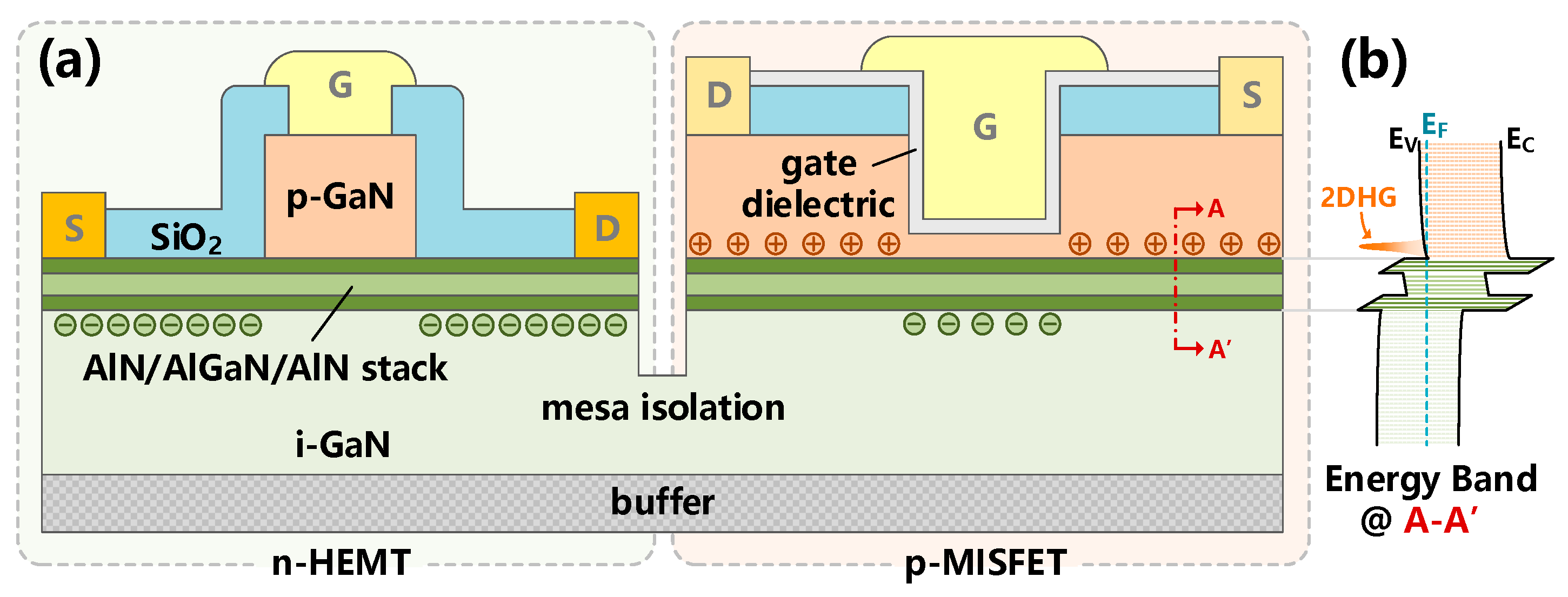
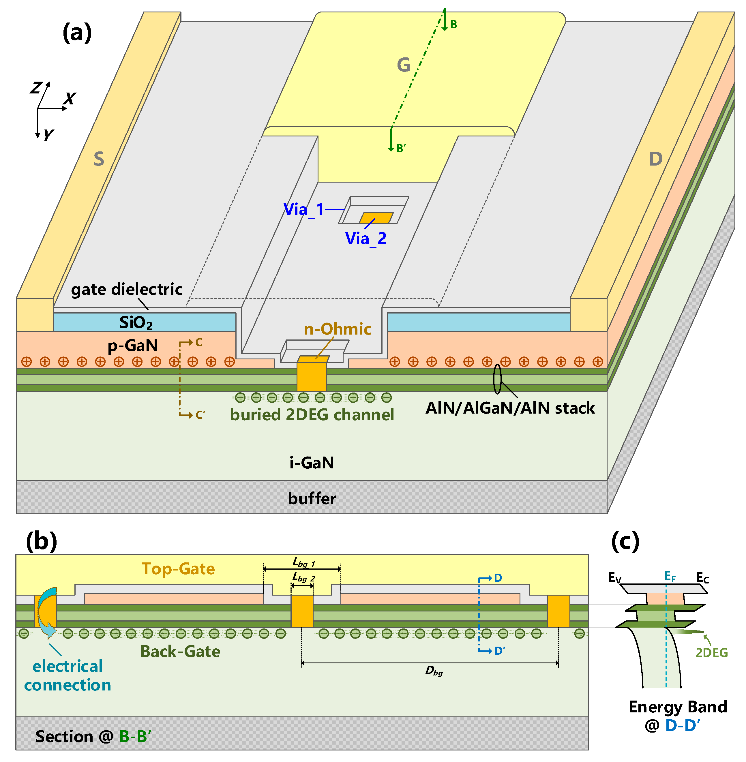
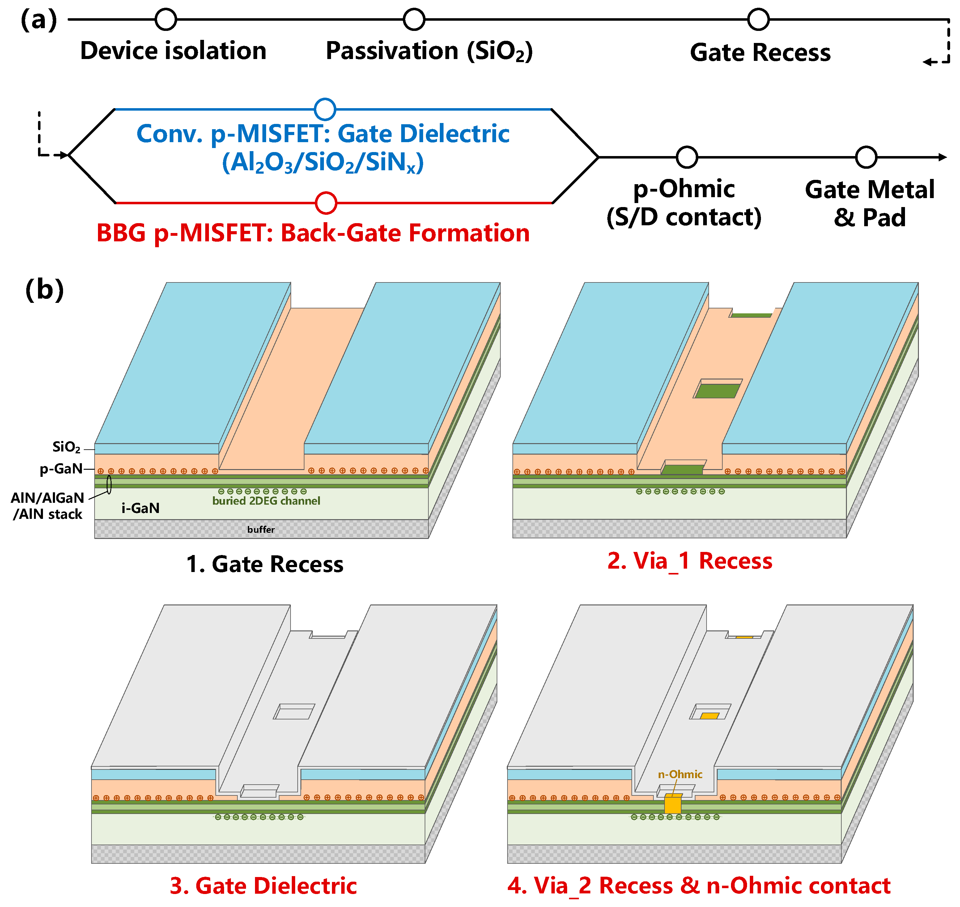
2. Double-Heterojunction Design and GaN p-MOSFET Device Structure

The p-GaN/AlN/AlGaN/AlN/GaN double heterojunction is designed to accommodate the p-type channel (2-DHG) at the upper p-GaN/AlN hetero-interface as well as the n-type channel (2-DEG) at the lower AlGaN/AlN/GaN hetero-interface. As shown in Figure 1, due to the existence of the top p-GaN cap, the buried 2-DEG channel can be depleted, leaving the upper 2-DHG channel to form the current conduction channel of the p-MISFET, which features the benefit of de-coupling the parasitic capacitance between the p/n-type channel and then enhancing the signal integrity of the realized CMOS IC. On the other hand, the buried 2-DEG channel can be regained by removing the top p-GaN cap layer in the access region, which enables the n-channel HEMT to be fabricated. Hence, both p-type and n-type devices can be fabricated on this double heterojunction, which enables single-chip CMOS integration.
The schematic device structure of the proposed BBG p-MISFET is shown in Figure 2. The trench gate is employed to fully deplete the 2DHG to achieve E-mode operation, while a very thin p-GaN (i.e., 5 nm) remains to maintain a high hole mobility within the E-mode channel. Due to the removal of the top p-GaN cap, the buried 2DEG channel is regained beneath the trench gate, which is similar to what was experimentally demonstrated in [31]. Such a regained high-density 2DEG channel beneath the upper hole channel can be electrically connected with the top metal gate terminal through the “distribute-recessed via” and performs as a back gate. Such a back gate together with the conventional top gate constructs a dual gate which is able to enhance the gate-to-channel modulation capability of the BBG p-MISFET. The simulation was conducted using Sentaurus TCAD with a generation–recombination model (SRH), a carrier mobility degradation model (with doping dependence and high field saturation), and a piezoelectric polarization model (strain). The key parameters of the device structure used in the simulation are listed in Table 1, and the physical parameters for TCAD simulation are listed in Table 2. These refer to typical values reported in recent studies to ensure the simulation credibility. The hole mobility (~10 cm2/V·s) is referenced from the typical channel mobility observed in recent reports based on a similar epitaxial structure [17,18,19]. According to the experiments in [32], the donor-like states of 2.5 × 1012 cm−2 were used to imitate the interface states at the dielectric/p-GaN interface introduced by gate trench etching. In order to calibrate the TCAD model, the simulated conventional GaN p-MISFET delivers a current density of ~2.1 mA/mm (@ VG = VD = −5 V) and SS of ~148 mV/dec, which are comparable to those values reported in [29,33]. The structural parameters, physical characteristics, and applied models for the proposed target device (i.e., BBG p-MISFET) are entirely consistent with those employed for the calibrated reference structure (i.e., conventional GaN p-MISFET).

3. Simulation Results and Discussion

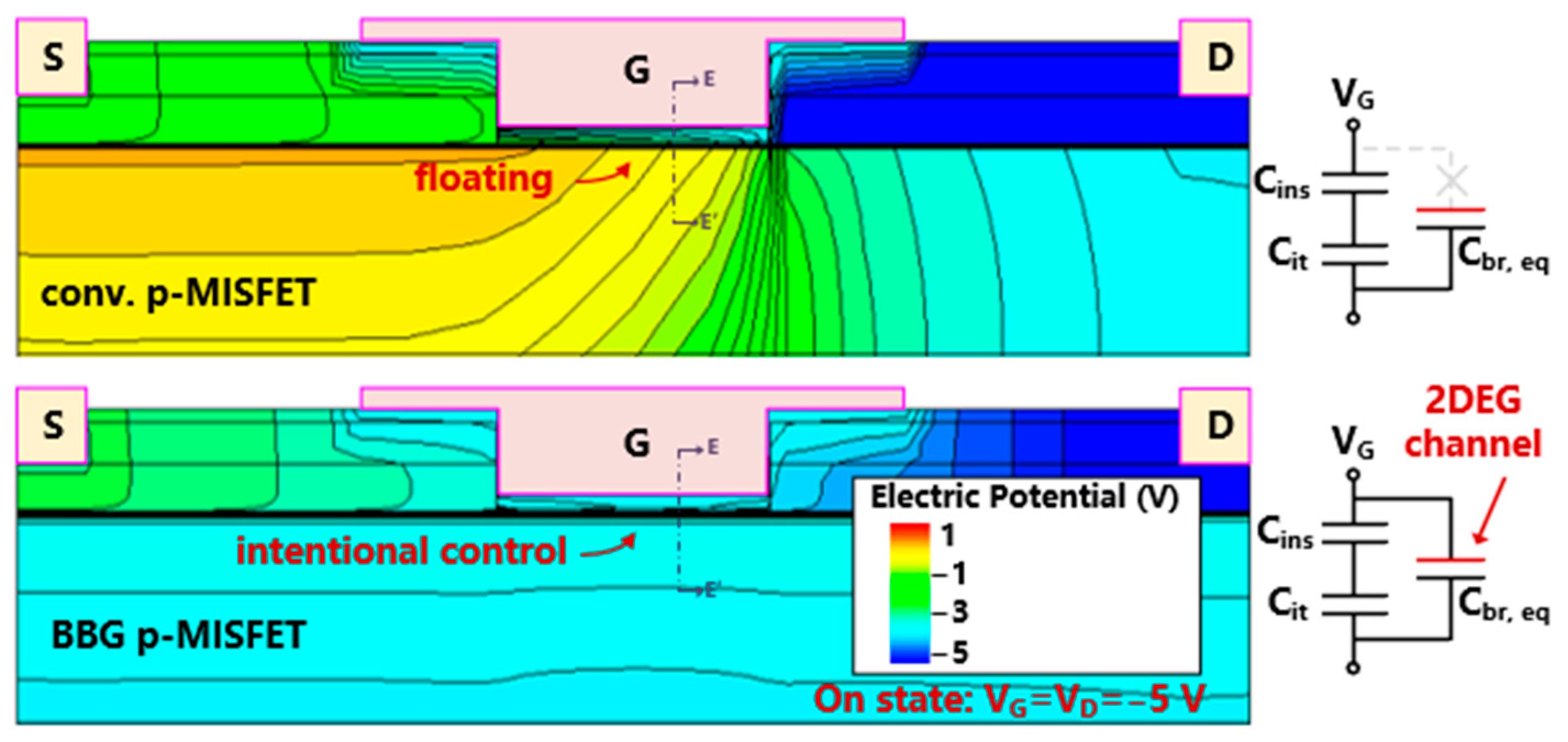
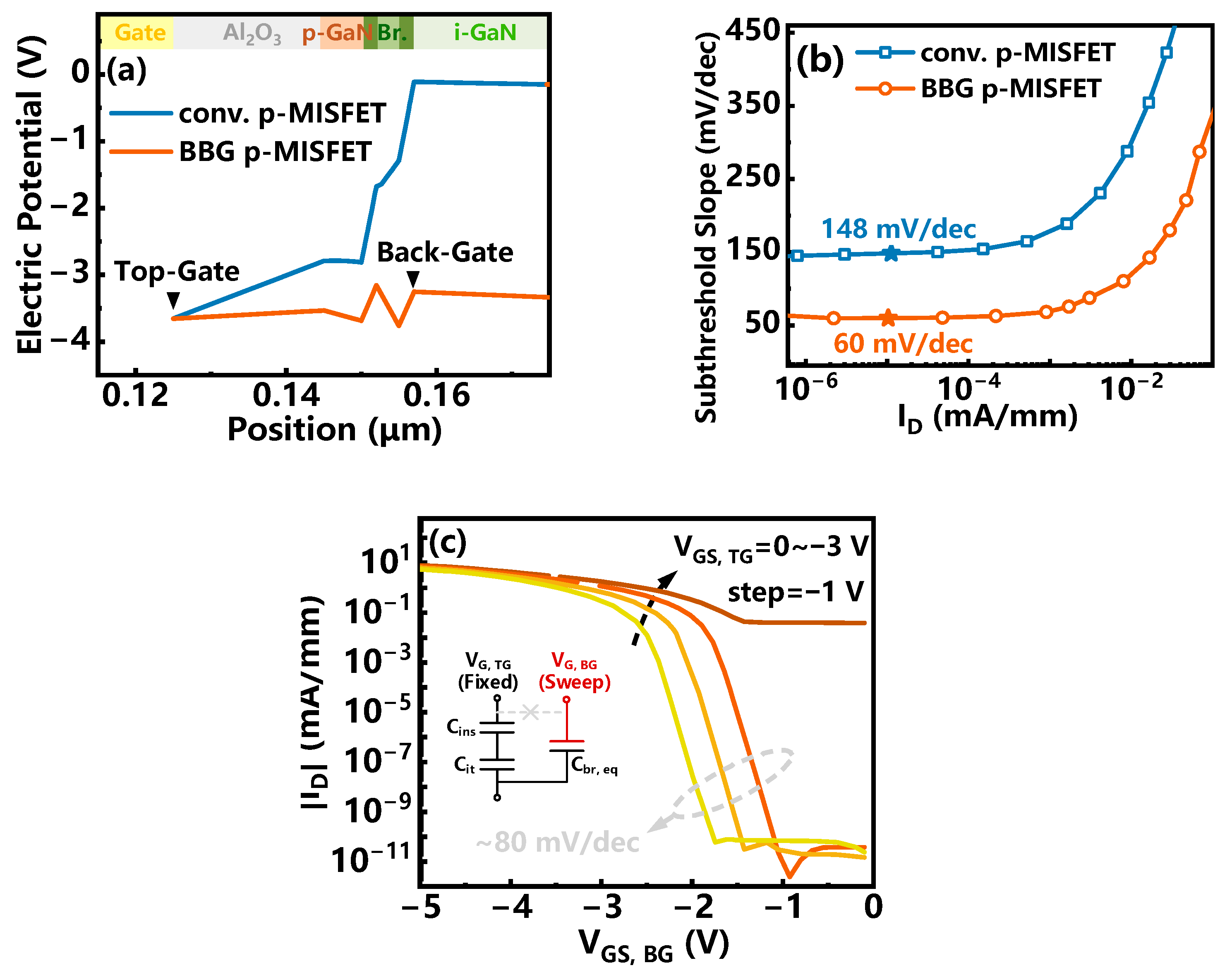
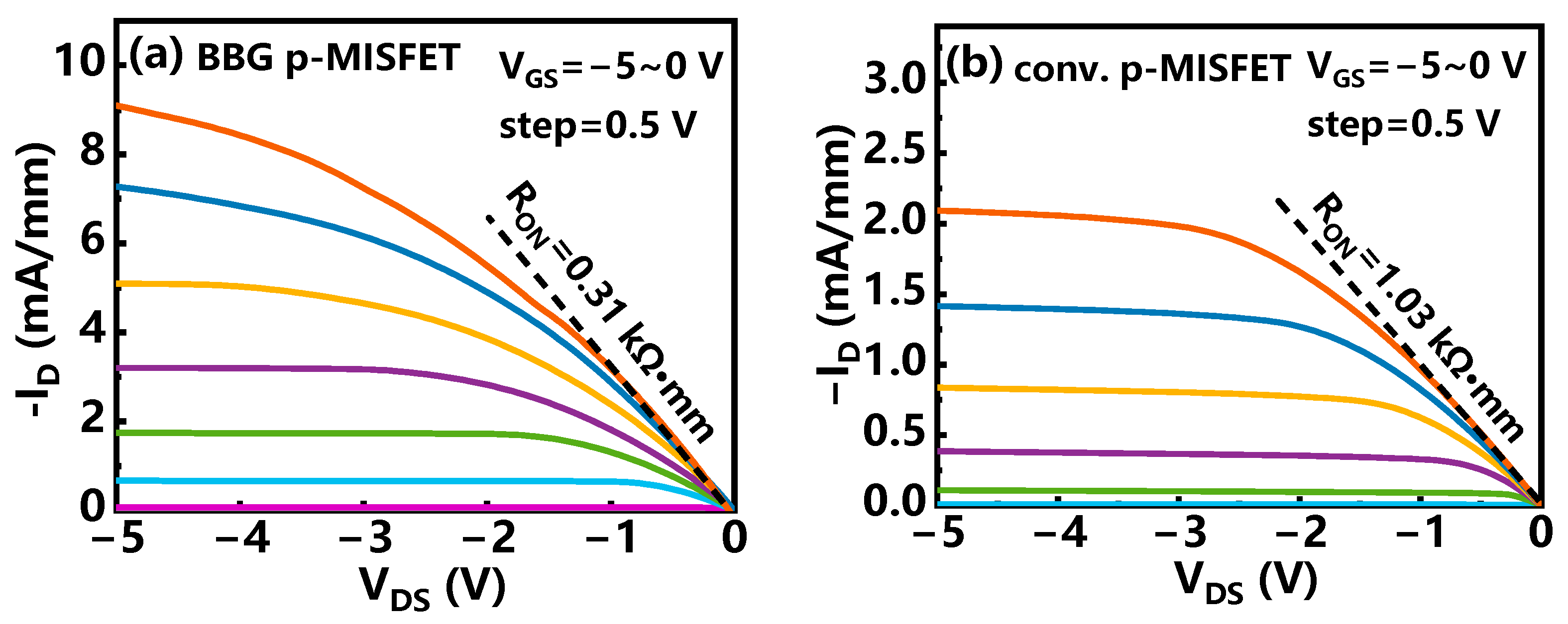
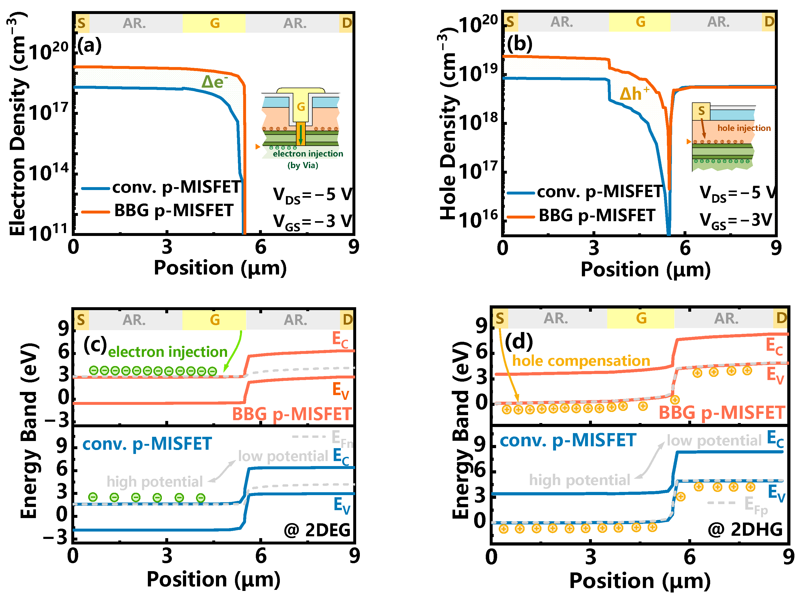
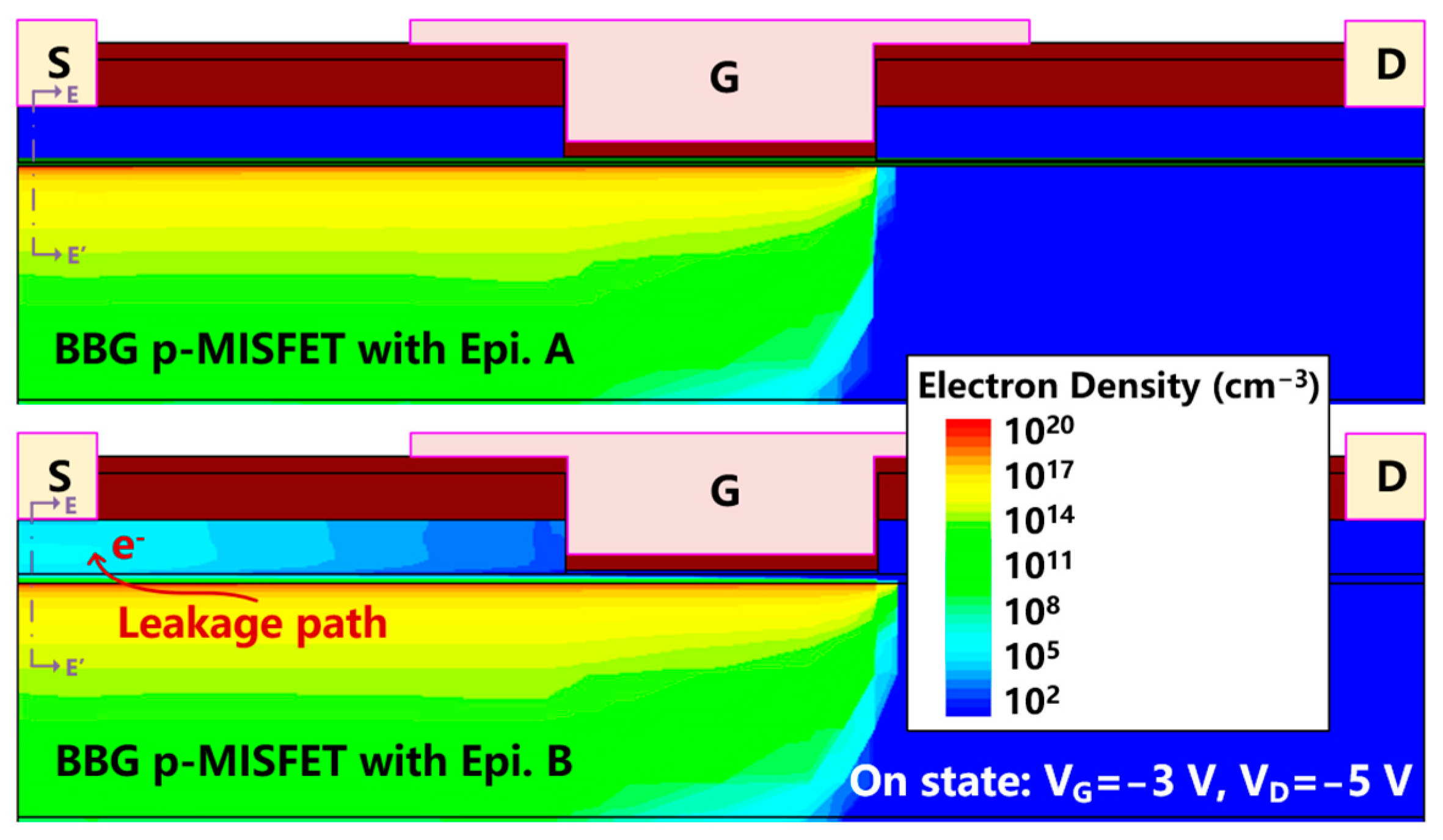
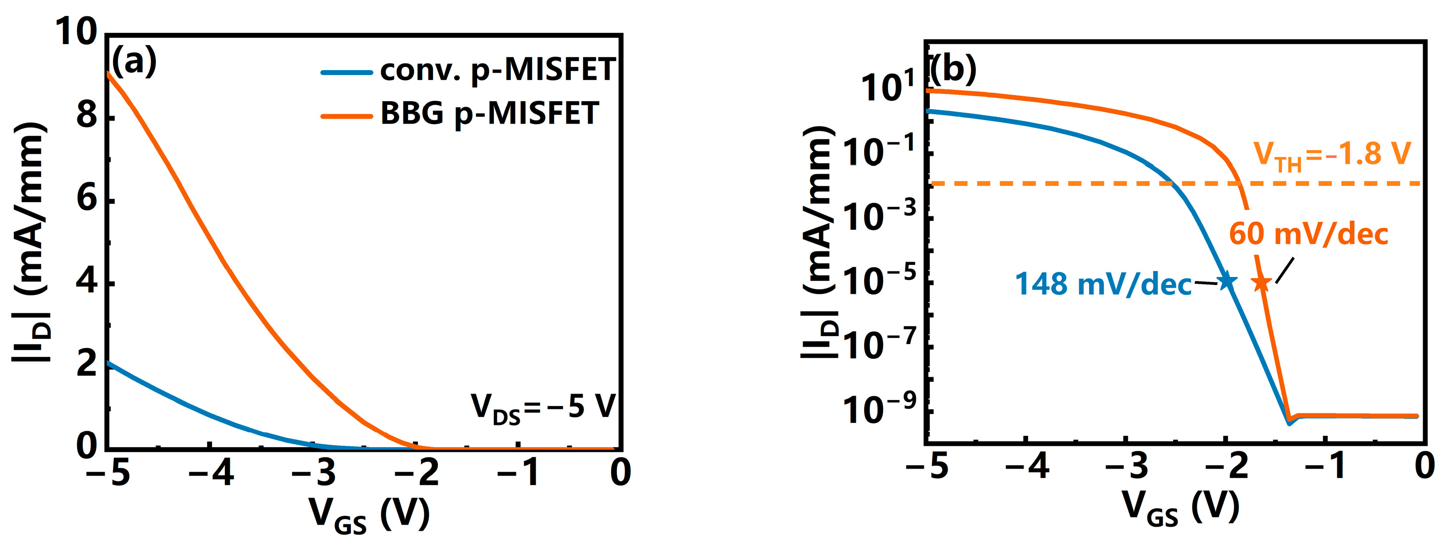
3.1. I-V Characteristics of the BBG p-MISFET

As shown in Figure 3, in the access region, the polarization-induced 2DHG of 1.5 × 1012 cm−2 was formed at the upper p-GaN/AlN hetero-interface to enhance the current transport of p-MISFET. In the trench gate, since the p-GaN cap was partially removed, the 2DEG channel beneath was regained at the lower AlN/GaN hetero-interface with a high density of ~2 × 1012 cm−2 that is comparable to the reported result [32]. Figure 4 illustrates a comparison of the transfer characteristics between the BBG p-MISFET and the conventional p-MISFET. At the same trench gate depth, the BBG p-MISFET exhibited an equivalent pinch-off voltage to that of the conventional device. As long as the trench gate depth satisfies the criteria for the formation of an intrinsic normally off channel (i.e., complete hole depletion under zero bias in the gate region), an enhancement-mode BBG p-MISFET can be realized. Notably, the subthreshold slope of the BBG p-MISFET was significantly lower than that of the typical conventional p-MISFET. For the conventional p-MISFETs, the regained 2DEG was floating, as shown in Figure 5, while its electric potential varied with the external bias voltage (e.g., VG and VD) and could not be intentionally controlled, which featured a negligible impact on the current transport in the upper p-channel at the p-GaN/AlN hetero-interface. In contrast, in the BBG p-MISFET, the buried 2DEG beneath the recessed gate region is connected to the top metal gate electrode, which acts as a back gate that is capable of enhancing the gate-to-channel modulation capability.
According to the derivation of SS for n-channel devices [34], the SScon for p-channel GaN MISFETs can be expressed as:
S S c o n = k T q l n 10 1 + C i t C i n s  
where k is the Boltzmann’s constant, T is the temperature, q is the electronic charge, Cins is the capacitance for the gate insulator, and Cit is the equivalent trap capacitance (particularly at the interface of dielectric/III-Nitride). For the BBG p-MISFET, the equivalent capacitance of the barrier layer Cbr,eq led to the synergistic variation in charge between the buried 2DEG channel and the upper p-channel, where the AlN/AlGaN/AlN stack can be considered a dielectric-like layer. Furthermore, the control of the p-channel by the 2DEG back gate was unaffected by the trapping/detrapping of interface states at the dielectric/III-Nitride interface (expressed as Cit), thus enabling an improved gate control capability. Thus, the double-gate (top metal gate and 2DEG back gate) structure fundamentally provides superior subthreshold characteristics over the conventional p-MISFET. As depicted in Figure 6b, the conventional p-MISFET exhibited a relatively large subthreshold slope of 148 mV/dec. In contrast, due to the improved gate control capability and the mitigation of the interface trap effect, the BBG p-MISFET achieved a subthreshold slope as low as ~60 mV/dec, which is only 40% that of the conventional device. To better illustrate the role of back gate control, Figure 6c further demonstrates the transfer curves assuming separate voltages are applied to the top gate and the back gate. Even with the top-gate voltage VGS,TG fixed, the back gate remained capable of independently turning the p-channel on and off. Under the fixed voltages of 0, −1, and −2 V applied to the top gate, the hole carriers in the p-channel could be depleted by the top-gate MIS structure. Nevertheless, independent control by the back gate still achieved a subthreshold slope of ~80 mV/dec, emphasizing the significant impact of back gate control. Thus, under normal device operation (where the top gate and back gate are turned on or off synchronously), the ultra-low subthreshold slope was maintained over a wide current range (~10−6–10−3 mA/mm) by the BBG p-MISFET, which is advantageous for enhancing the device switching speed and reducing the circuit response time. Furthermore, it allows the device to operate at lower voltages, thereby achieving reduced system power consumption.
The output characteristics of the BBG p-MISFET and conventional p-MISFET are shown in Figure 7a and Figure 7b, respectively. A considerable ID of 9.1 mA/mm and a low RON of 0.31 kΩ·mm were achieved with a buried 2DEG back gate, representing improvements of 330% in ID and 70% in RON compared with conventional GaN p-MISFETs. As depicted in Figure 8, as the source terminal was biased at a high potential, the electrons within the buried 2DEG channel beneath the gate region were attracted by the relatively high electric potential of the source and accumulated in the gate-to-source access region. Because the buried 2DEG channel was floating in the conventional GaN p-MISFET, its electron density did not change with the external bias voltage. In contrast, in the BBG p-MISFET, together with the more negative gate bias when the device was turned on and off, additional electrons were injected in the buried 2DEG channel from the top metal gate electrode for electric potential compensation in order to maintain the equal electric potential of the top metal gate and the buried 2DEG back gate. To maintain the charge equilibrium between the buried 2DEG channel and the upper p-channel, additional hole carriers were correspondingly injected from the source electrode into the p-channel. Under the joint influence of the back gate effect and the hole compensation behavior, the drain current density in the BBG p-MISFET was substantially improved.
On the other hand, it should be noted that a vertical leakage from p-channel to n-channel may occur when high gate bias voltage is applied, which was reported in a previous study [32]. To mitigate the vertical leakage, an AlN/AlGaN/AlN stack (Epi. A) was used instead of the single-layer AlGaN barrier (Epi. B), which demonstrated promising results in suppressing vertical leakage, as shown in Figure 9. It was revealed that electrons can pass through the AlGaN barrier (Epi. B) and recombine with holes located beneath the source electrode in the p-channel under on-state conditions (i.e., VG = −3 V, VD = −5 V). However, this did not occur for the composite AlN/AlGaN/AlN barrier (Epi. A). Due to the large bandgap of AlN, as portrayed in Figure 10a, the conduction band offset and valence band offset were elevated from 0.4 to 1.95 eV for the conduction band and from 0.15 to 0.8 eV for the valence band. Thus, the AlN layers could effectively suppress carrier tunneling between the upper p-channel and the lower buried 2DEG channel. Compared with the single-layer AlGaN barrier, the design of the composite AlN/AlGaN/AlN barrier significantly reduced vertical leakage by more than three orders of magnitude. It enables the BBG p-MISFET to feature a large effective gate swing that allows the device to deliver a high performance.
The performance of the proposed BBG p-MISFET device is summarized in Table 3 and compared with that of the conventional device, as well as a representative GaN p-MISFET reported in the literature. It is further indicated that the BBG p-MISFET represents a highly promising technology solution capable of concurrently achieving high current density and low subthreshold slope.

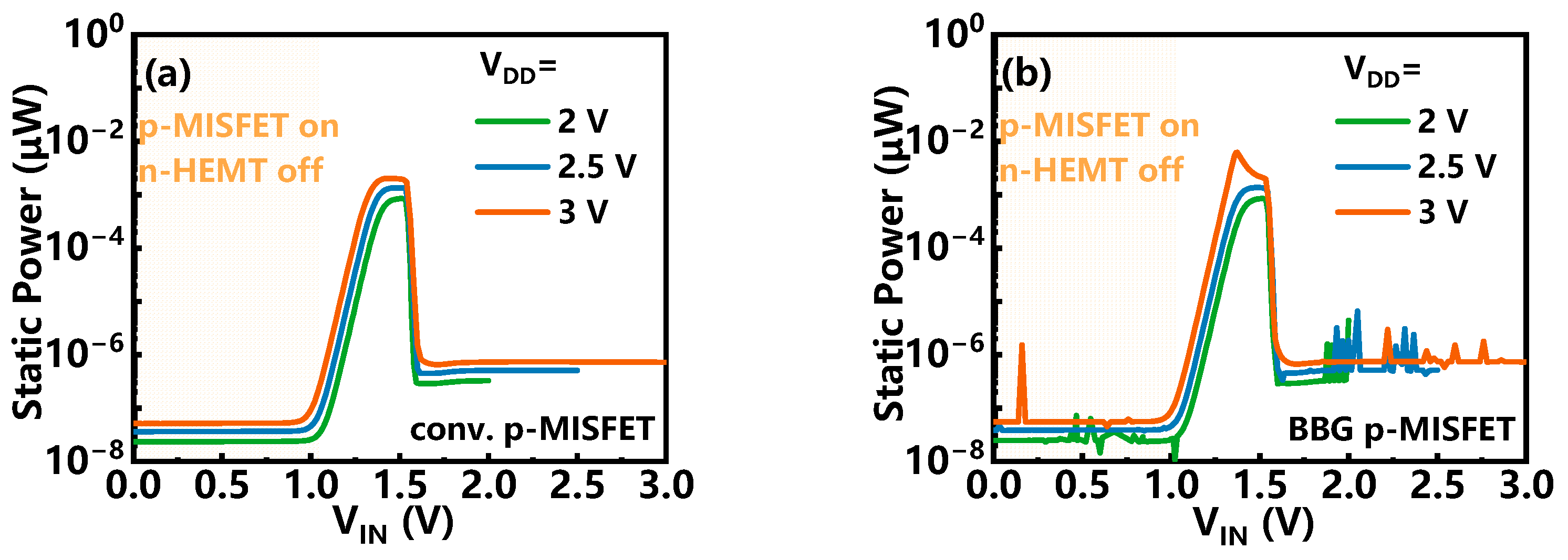
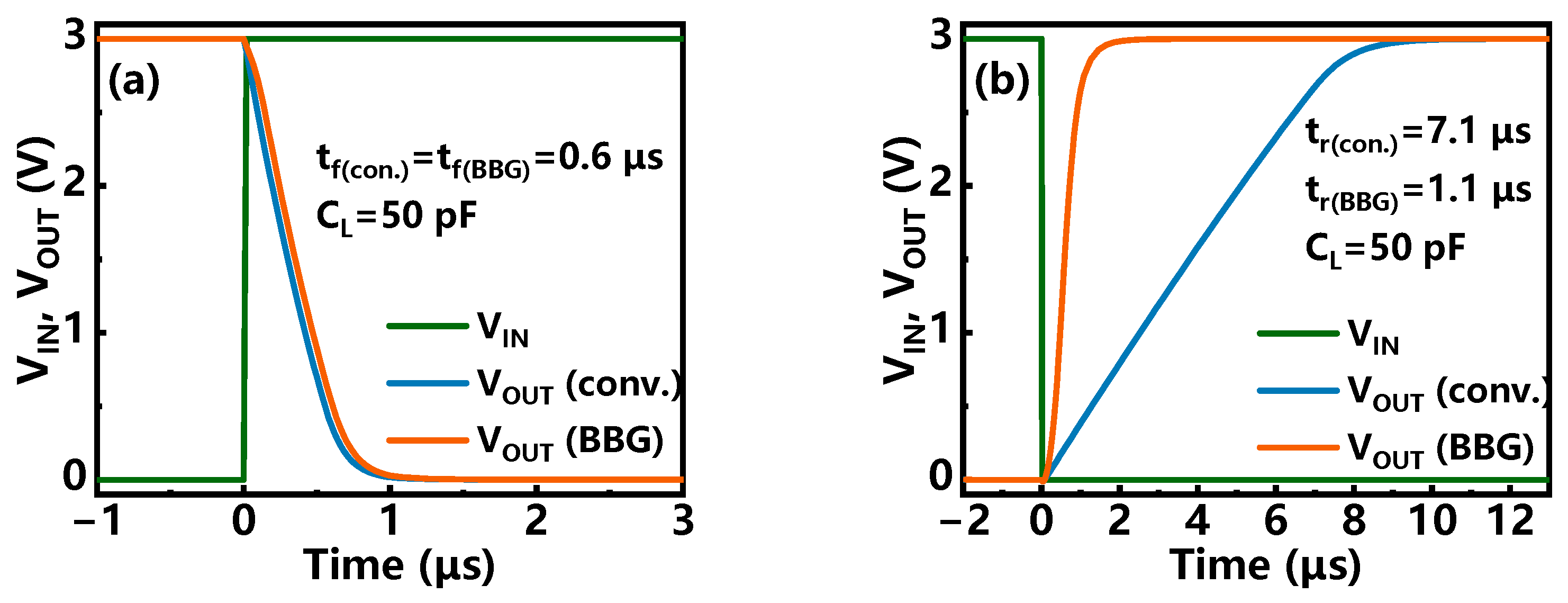
3.2. Switching Characteristics of the Complementary Logic Inverters

The performance improvement obtained in the BBG p-MISFET was further validated by using the device in a CMOS inverter circuit by mixed-mode simulation. It should be pointed out that the complementary n-type device was also demonstrated and simulated based on the heterojunction structure with the AlN/AlGaN/AlN stack, which reinforces the concept of single-chip CMOS integration of the proposed BBG p-MISFET. Figure 11a,b illustrate the transfer and output characteristics of the n-type enhancement-mode GaN HEMT. When using the identical parameter configuration shown in Table 1 and Table 2, the VTH, SS, and RON of the GaN n-HEMT were 1.4 V, 68 mV/dec, and 0.036 kΩ·mm, respectively. The significantly improved SS achieved in BBG p-MISFET allows the device to be implemented in high-speed and low-supply-voltage applications. In subsequent mixed-mode simulations, a width-to-length ratio of 20/200 μm was selected, which is typically employed in reported works involving the monolithic integration of GaN p-MISFETs and n-HEMTs [16].
Figure 12a,b compare the transfer characteristics (VTCs) of the CL inverters based on the conventional p-MISFET and BBG p-MISFET, respectively. A substantially high peak voltage gain of 20.8 v/v obtained at Vm of 1.38 V was extracted from the CL inverter based on the BBG p-MISFET, which is superior to the voltage gain of 13.4 v/v found for the conventional p-MISFET. Accordingly, the CL inverter based on the BBG p-MISFET exhibits a better noise margin, which ensures a higher noise immunity performance. Thus, the CL inverters with BBG p-MISFET can accommodate a larger range of input voltages with higher robustness against process variations and temperature fluctuations. Figure 13a,b illustrate the static power consumption of the CL inverters based on the conventional p-MISFET and the BBG p-MISFET with varied VIN and VDD. At a low VIN, the p-MISFET was turned on, and the n-HEMT was turned off, thereby resulting in minimal static power dissipation. The comparison reveals that the BBG p-MISFET maintained consistently low static power consumption owing to the effectively suppressed vertical leakage current by using an AlN/AlGaN/AlN heterostructure. For VDD = −3 V, the VTH of the BBG p-MISFET exhibited a slight rightward drift compared with the conventional p-MISFET, leading to a minor increase in quasi-static power consumption during level shifting, which was negligible at lower VDD. The results underscore the suitability of the BBG p-MISFET for high-speed and low-power switching applications with a low operation voltage.
The dynamic switching characteristics of the CL inverters are shown in Figure 14a,b, in which the fall time tf is defined as the duration it takes for VOUT to decrease from 90% to 10% of VDD and the rise time tr is defined as the duration it takes for VOUT to increase from 10% to 90% of VDD. The fall time tf for either of the inverters based on the BBG p-MISFET and conventional p-MISFET was 0.6 μs, which was determined using the GaN n-HEMT. Meanwhile, compared with the conventional p-MISFET based on a CL inverter, the rise time tr was significantly reduced from 7.1 μs to 1.1 μs with BBG p-MISFET, which allows for a respectably enhanced current drive capability.
Overall, the BBG p-MISFET delivers a superior performance in the dynamic switching process of the CL inverter compared with the conventional p-MISFET. It can be anticipated that the proposed BBG p-MISFET, if employed in system-level CMOS control circuits, will result in significant optimization of their response speed and chip area. Firstly, the reduction in SS (from 148 mV/dec to ~60 mV/dec) enables the CL inverter unit to exhibit a steeper transfer characteristic, which results in larger noise margin and is capable of improving the noise sensitivity of the system. Moreover, a higher voltage gain ensures a rapid response of the output signal to the input signal. Secondly, the enhanced current drive capability of the BBG p-MISFET significantly reduces the tr of the CL inverter (from 7.1 μs to 1.1 μs), which further elevates the signal system response speed. Additionally, recent reports of the monolithic integration of p-channels and n-channels always address the weaker current density of the p-MISFET by enlarging the device footprint, which leads to a substantial increase in the overall chip area. Thus, the BBG p-MISFET enables a more favorable trade-off between chip area and system response speed. The results of mixed-mode simulation showcase the exceptional compatibility of the BBG p-MISFET with low-voltage logic circuits, suggesting its potential to serve as a novel structure for further advancing the development of high-speed and low-power GaN monolithic integration technology.
In addition, Figure 15 illustrates the process flowchart of the proposed BBG p-MISFET. Due to the substantially higher temperature (~830 °C) [36] required for the formation of n-type ohmic contact compared with the formation of p-type ohmic contact (~550 °C) [36], a “gate-first” approach is accordingly proposed for fabricating the BBG p-MISFET. This involves utilizing electron beam lithography to form the “distribute-recessed via” at the bottom of the conventional gate trench, followed by the realization of n-ohmic contact for back gate (along with ohmic contacts for the integrated n-channel devices) at high temperatures. After that, the remaining low-temperature processing steps are conducted, which is consistent with the typical process sequence for conventional GaN p-MISFETs, as reported in experimental works [38]. All the aforementioned steps are compatible with the current process of fabricating commercial n-channel p-GaN gate HEMTs.

4. Conclusions

In this study, based on a double-heterostructure p-GaN/AlN/AlGaN/AlN/GaN, a novel enhancement-mode GaN p-MISFET utilizing the intrinsic buried 2DEG channel beneath the recessed gate performing as the back gate is demonstrated. Compared with conventional GaN p-MISFETs, the proposed BBG p-MISFET exhibited significant improvement in subthreshold characteristics and current drive capability. An ultra-low SS of ~60 mV/dec (vs. ~148 mV/dec in the conv. device) and a respectably high ID of −9.1 mA/mm (vs. −2.1 mA/mm in the conv. device) were achieved with the BBG p-MISFET. With in-depth analysis, the enhancement of the subthreshold and on-state characteristics of the device due to the back gate effect and hole compensation behavior was profoundly elucidated. Furthermore, the mixed-mode simulation of the CL inverter based on the BBG p-MISFET showed excellent transfer and dynamic switching characteristics. In comparison with conventional GaN p-MISFETs, the voltage gain increased from 13.4 v/v to 20.8 v/v, and the rise time tr dramatically decreased from 7.1 µs to 1.1 µs. In general, the proposed BBG p-MISFET shows great potential for high-speed and low-power GaN monolithic integration technology.

Author Contributions

Conceptualization, H.W. and K.C.; software, H.W., J.Z., K.C. and Y.Z.; investigation, H.W., K.C., S.H. and Q.Z.; writing—original draft preparation, H.W. and K.C.; writing—review and editing, Q.Z., E.D., N.Y. and B.Z.; supervision, Q.Z.; project administration, Q.Z. and B.Z. All authors have read and agreed to the published version of the manuscript.

Funding

This work was supported in part by the National Natural Science Foundation of China under Grant 62174019, in part by the Guangdong Basic and Applied Basic Research Foundation under Grant 2021B1515140039, and in part by Sichuan Science and Technology Program under Grant 2023YFG0138.

Data Availability Statement

The data presented in this study are available on request from the corresponding author. The data are not publicly available due to privacy.

Conflicts of Interest

The authors declare no conflict of interest.

References

  1. Chow, T.P. Progress in High Voltage SiC and GaN Power Switching Devices. Mater. Sci. Forum 2014, 778–780, 1077–1082. [Google Scholar] [CrossRef]
  2. Chen, K.J.; Häberlen, O.; Lidow, A.; lin Tsai, C.; Ueda, T.; Uemoto, Y.; Wu, Y. GaN-on-Si Power Technology: Devices and Applications. IEEE Trans. Electron Devices 2017, 63, 779–795. [Google Scholar] [CrossRef]
  3. Meneghini, M.; De Santi, C.; Abid, I.; Buffolo, M.; Cioni, M.; Khadar, R.A.; Nela, L.; Zagni, N.; Chini, A.; Medjdoub, F.; et al. GaN-based power devices: Physics, reliability, and perspectives. J. Appl. Phys. 2021, 130, 181101. [Google Scholar] [CrossRef]
  4. Su, M.; Chen, C.; Rajan, S. Prospects for the application of GaN power devices in hybrid electric vehicle drive systems. Semicond. Sci. Technol. 2013, 28, 074012. [Google Scholar] [CrossRef]
  5. Apparao, D.; Ghaffari, R.; Venkatesh, B.; Wu, B. A survey on energy storage technologies in power systems. In Proceedings of the 2015 IEEE Electrical Power and Energy Conference (EPEC), London, UK, 26–28 October 2015; pp. 105–111. [Google Scholar]
  6. Krichen, M.; Basheer, Y.; Qaisar, S.M.; Waqar, A. A Survey on Energy Storage: Techniques and Challenges. Energies 2023, 16, 2271. [Google Scholar] [CrossRef]
  7. Pearton, S.J.; Aitkaliyeva, A.; Xian, M.; Ren, F.; Khachatrian, A.; Ildefonso, A.; Islam, Z.; Rasel, M.A.J.; Haque, A.; Polyakov, A.Y.; et al. Radiation damage in wide and ultra-wide bandgap semiconductors. ECS J. Solid State Sci. Technol. 2021, 10, 055008. [Google Scholar] [CrossRef]
  8. Wong, K.-Y.; Chen, W.; Chen, K.J. Integrated Voltage Reference Generator for GaN Smart Power Chip Technology. IEEE Trans. Electron Devices 2010, 57, 952–955. [Google Scholar] [CrossRef]
  9. Kinzer, D. Monolithic GaN Power IC Technology Drives Wide Bandgap Adoption. In Proceedings of the 2020 IEEE International Electron Devices Meeting (IEDM), San Francisco, CA, USA, 12–16 December 2020; pp. 27.5.1–27.5.4. [Google Scholar]
  10. Cui, M.; Sun, R.; Bu, Q.; Liu, W.; Wen, H.; Li, A.; Liang, Y.C.; Zhao, C. Monolithic GaN Half-Bridge Stages With Integrated Gate Drivers for High Temperature DC-DC Buck Converters. IEEE Access 2019, 7, 184375–184384. [Google Scholar] [CrossRef]
  11. Li, F.; Li, A.; Wang, Y.; Zhu, Y.; Yu, C.; Ding, C.; Wu, S.; Liu, W.; Yu, G.; Gao, X.; et al. Demonstration of the Hydrogen Passivated GaN HEMTs IC Platform. In Proceedings of the 35th International Symposium on Power Semiconductor Devices and ICs (ISPSD), Hong Kong, China, 28 May–1 June 2023; pp. 99–102. [Google Scholar]
  12. Li, X.; Geens, K.; Amirifar, N.; Zhao, M.; You, S.; Posthuma, N.; Liang, H.; Groeseneken, G.; Decoutere, S. Integration of GaN analog building blocks on p-GaN wafers for GaN ICs. J. Semicond. 2021, 42, 117–120. [Google Scholar] [CrossRef]
  13. Tang, G.; Kwan, A.M.H.; Wong, R.K.Y.; Lei, J.; Su, R.Y.; Yao, F.W.; Lin, Y.M.; Yu, J.L.; Tsai, T.; Tuan, H.C.; et al. Digital Integrated Circuits on an E-Mode GaN Power HEMT Platform. IEEE Electron Device Lett. 2017, 38, 1282–1285. [Google Scholar] [CrossRef]
  14. Li, X.; Amirifar, N.; Geens, K.; Zhao, M.; Guo, W.; Liang, H.; You, S.; Posthuma, N.; De Jaeger, B.; Stoffels, S.; et al. GaN-on-SOI: Monolithically integrated all-GaN ICs for power conversion. In Proceedings of the 2019 IEEE International Electron Devices Meeting (IEDM), Francisco, CA, USA, 7–11 December 2019. [Google Scholar]
  15. Zheng, Z.; Zhang, L.; Song, W.; Feng, S.; Xu, H.; Sun, J.; Yang, S.; Chen, T.; Wei, J.; Chen, K.J. Gallium nitride-based complementary logic integrated circuits. Nat. Electron. 2021, 4, 595–603. [Google Scholar] [CrossRef]
  16. Zheng, Z.; Song, W.; Zhang, L.; Yang, S.; Wei, J.; Chen, K.J. Monolithically Integrated GaN Ring Oscillator Based on High-Performance Complementary Logic Inverters. IEEE Electron Device Lett. 2021, 42, 26–29. [Google Scholar] [CrossRef]
  17. Poncé, S.; Jena, D.; Giustino, F. Route to High Hole Mobility in GaN via Reversal of Crystal-Field Splitting. Phys. Rev. Lett. 2019, 123, 096602. [Google Scholar] [CrossRef] [PubMed]
  18. Chowdhury, N.; Lemettinen, J.; Xie, Q.; Zhang, Y.; Rajput, N.S.; Xiang, P.; Cheng, K.; Suihkonen, S.; Then, H.W.; Palacios, T. P-Channel GaN Transistor Based on p-GaN/AlGaN/GaN on Si. IEEE Electron Device Lett. 2019, 40, 1036–1039. [Google Scholar] [CrossRef]
  19. Zhu, L.Y.; Chen, K.L.; Ma, Y.; Cai, Y.; Zhou, C.H.; Li, Z.J.; Zhang, B.; Zhou, Q. High threshold voltage enhancement-mode GaN p-FET with Si-rich LPCVD SiNx gate insulator for high hole mobility. J. Semicond. 2023, 44, 082801. [Google Scholar] [CrossRef]
  20. Zheng, Z.; Zhang, L.; Song, W.; Chen, T.; Feng, S.; Ng, Y.H.; Sun, J.; Xu, H.; Yang, S.; Wei, J.; et al. Threshold Voltage Instability of Enhancement-Mode GaN Buried p-Channel MOSFETs. IEEE Electron Device Lett. 2021, 42, 1584–1587. [Google Scholar] [CrossRef]
  21. Chowdhury, N.; Xie, Q.; Niroula, J.; Rajput, N.S.; Cheng, K.; Then, H.W.; Palacios, T. Field-induced acceptor ionization in enhancement-mode GaN p-MOSFETs. In Proceedings of the 2020 IEEE International Electron Devices Meeting (IEDM), San Francisco, CA, USA, 12–16 December 2020. [Google Scholar]
  22. Zhang, Y.; Sun, Z.; Wang, W.; Liang, Y.; Cui, M.; Zhao, Y.; Wen, H.; Liu, W. Low-resistance Ni/Ag contacts on GaN-based p-channel heterojunction field-effect transistor. IEEE Trans. Electron Devices 2022, 70, 31–35. [Google Scholar] [CrossRef]
  23. Tang, C.-Y.; Lu, H.-H.; Qiao, Z.-P.; Jiang, Y.; Du, F.-Z.; He, J.-Q.; Jiang, Y.-L.; Wang, Q.; Yu, H.-Y. Ohmic contact with a contact resistivity of 12 Ω mm on p-GaN/AlGaN/GaN. IEEE Electron Device Lett. 2022, 43, 1412–1415. [Google Scholar] [CrossRef]
  24. Bader, S.J.; Chaudhuri, R.; Nomoto, K.; Hickman, A.; Chen, Z.; Then, H.W.; Muller, D.A.; Xing, H.G.; Jena, D. Gate-Recessed E-mode p-Channel HFET With High On-Current Based on GaN/AlN 2D Hole Gas. IEEE Electron Device Lett. 2018, 39, 1848–1851. [Google Scholar] [CrossRef]
  25. Zhang, Z.; Encomendero, J.; Chaudhuri, R.; Cho, Y.; Protasenko, V.; Nomoto, K.; Lee, K.; Toita, M.; Xing, H.G.; Jena, D. Polarization-induced 2D hole gases in pseudomorphic undoped GaN/AlN heterostructures on single-crystal AlN substrates. Appl. Phys. Lett. 2021, 119, 162104. [Google Scholar] [CrossRef]
  26. Chowdhury, N.; Xie, Q.; Yuan, M.; Cheng, K.; Then, H.W.; Palacios, T. Regrowth-free GaN-based complementary logic on a Si substrate. IEEE Electron Device Lett. 2020, 41, 820–823. [Google Scholar] [CrossRef]
  27. Raj, A.; Krishna, A.; Romanczyk, B.; Hatui, N.; Liu, W.; Keller, S.; Mishra, U.K. GaN/AlGaN Superlattice Based E-Mode Hole Channel FinFET With Schottky Gate. IEEE Electron Device Lett. 2022, 44, 9–12. [Google Scholar] [CrossRef]
  28. Chowdhury, N.; Xie, Q.; Palacios, T. Self-Aligned E-Mode GaN p-Channel FinFET With ION> 100 mA/mm and ION/IOFF> 107. IEEE Electron Device Lett. 2022, 43, 358–361. [Google Scholar] [CrossRef]
  29. Yang, C.; Fu, H.; Peri, P.; Fu, K.; Yang, T.-H.; Zhou, J.; Montes, J.; Smith, D.J.; Zhao, Y. Enhancement-mode gate-recess-free GaN-based p-channel heterojunction field-effect transistor with ultra-low subthreshold swing. IEEE Electron Device Lett. 2021, 42, 1128–1131. [Google Scholar] [CrossRef]
  30. Yin, Y.; Lee, K.B. High-Performance Enhancement-Mode p-Channel GaN MISFETs With Steep Subthreshold Swing. IEEE Electron Device Lett. 2022, 43, 533–536. [Google Scholar] [CrossRef]
  31. Zheng, Z.; Chen, T.; Zhang, L.; Song, W.; Chen, K.J. Unveiling the parasitic electron channel under the gate of enhancement-mode p-channel GaN field-effect transistors on the p-GaN/AlGaN/GaN platform. Appl. Phys. Lett. 2022, 120, 152102. [Google Scholar] [CrossRef]
  32. Sang, L.; Ren, B.; Nabatame, T.; Sumiya, M.; Liao, M. Insight into traps at Al2O3/p-GaN metal-oxide-semiconductor interface fabricated on free-standing GaN substrate. J. Alloys Compd. 2021, 853, 157356. [Google Scholar] [CrossRef]
  33. Zheng, Z.; Song, W.; Zhang, L.; Yang, S.; Wei, J.; Chen, K.J. High ION and ION/IOFF Ratio Enhancement-Mode Buried p-Channel GaN MOSFETs on p-GaN Gate Power HEMT Platform. IEEE Trans. Electron Devices 2020, 41, 26–29. [Google Scholar] [CrossRef]
  34. Lyu, J.-S. A New Method for Extracting Interface Trap Density in Short-Channel MOSFETs from Substrate-Bias-Dependent Subthreshold Slopes. ETRI J. 1993, 15, 10–25. [Google Scholar] [CrossRef]
  35. Du, H.; Liu, Z.; Hao, L.; Su, H.; Zhang, T.; Zhang, W.; Zhang, J.; Hao, Y. High-performance E-mode p-channel GaN FinFET on silicon substrate with high I ON/I OFF and high threshold voltage. IEEE Electron Device Lett. 2022, 43, 705–708. [Google Scholar] [CrossRef]
  36. Chen, J.; Liu, Z.; Wang, H.; He, Y.; Zhu, X.; Ning, J.; Zhang, J.; Hao, Y. A GaN complementary FET inverter with excellent noise margins monolithically integrated with power gate-injection HEMTs. IEEE Trans. Electron Devices 2021, 69, 51–56. [Google Scholar] [CrossRef]
  37. Chu, R.; Cao, Y.; Chen, M.; Li, R.; Zehnder, D. An Experimental Demonstration of GaN CMOS Technology. IEEE Electron Device Lett. 2016, 37, 269–271. [Google Scholar] [CrossRef]
  38. Jin, H.; Jiang, Q.; Huang, S.; Wang, X.; Wang, Y.; Ji, Z.; Dai, X.; Feng, C.; Fan, J.; Wei, K.; et al. An Enhancement-Mode GaN p-FET With Improved Breakdown Voltage. IEEE Electron Device Lett. 2022, 43, 1191–1194. [Google Scholar] [CrossRef]
Figure 1. (a) The schematic diagram of monolithic integration of n-HEMT and p-MISFET based on a p-GaN/AlN/AlGaN/AlN/GaN double heterojunction. (b) The schematic energy-band diagram along the cutline A-A’ in the access region.
Electronics 13 00729 g001
Figure 2. (a) The schematic structure of GaN p-MISFET featuring a buried back gate (BBG p-MISFET). (b) The cross-sectional view along the cutline B-B’ in the gate region. (c) The schematic energy-band diagram along the cutline D-D’ in the gate region.
Electronics 13 00729 g002
Figure 3. The simulated energy band and hole/electron density of the proposed BBG p-MISFET along the cutline (a) C-C’ in the access region and (b) D-D’ in the gate region.
Electronics 13 00729 g003
Figure 4. The transfer characteristics of BBG p-MISFET and conventional GaN p-MISFET (conv. p-MISFET) in (a) linear and (b) semi-log coordinates.
Electronics 13 00729 g004
Figure 5. The electric potential distribution and equivalent circuit diagram of the BBG p-MISFET and the conventional p-MISFET.
Electronics 13 00729 g005
Figure 6. (a) The gate region electric potential distribution along the cutline D-D’ and (b) the SS vs. ID plot of the BBG p-MISFET and the conventional p-MISFET. (c) The back gate control-only transfer characteristics curve under independent voltage stress of the top gate and the back gate (VGS,TG fixed while sweeping VGS,BG).
Electronics 13 00729 g006
Figure 7. The output characteristics of (a) the BBG p-MISFET and (b) the conventional p-MISFET.
Electronics 13 00729 g007
Figure 8. (a) The simulated electron density along the 2DEG channel and (b) hole density along the 2DHG channel of the BBG p-MISFET and the conventional p-MISFET, (c) the simulated energy band along the 2DEG channel and (d) the simulated energy band along the 2DHG channel of the BBG p-MISFET and the conventional p-MISFET (AR. refers to access region).
Electronics 13 00729 g008
Figure 9. The electron distribution of the BBG p-MISFETs with a 2/3/2 nm AlN/AlGaN/AlN stack barrier (Epi. A) and 12 nm AlGaN barrier (Epi. B) (VG = −3 V, VD = −5 V).
Electronics 13 00729 g009
Figure 10. (a) The simulated energy band along the cutline E-E’ (VG = VD = 0 V) and (b) gate leakage characteristics of the BBG p-MISFETs with an AlN/AlGaN/AlN stack barrier (Epi. A) and 12 nm AlGaN barrier (Epi. B).
Electronics 13 00729 g010
Figure 11. (a) The transfer characteristics and (b) output characteristics of the n-channel GaN HEMT based on the same heterostructure with p-channel GaN MISFETs.
Electronics 13 00729 g011
Figure 12. The VIN-VOUT transfer characteristics and voltage gain of the CL inverters (Wn/Wp = 20 μm/200 μm) based on (a) the conventional p-MISFET and (b) the BBG p-MISFET.
Electronics 13 00729 g012
Figure 13. The quasi-static power consumption of the CL inverters (Wn/Wp = 20 μm/200 μm) with varied supply voltage VDD based on (a) the conventional p-MISFET and (b) the BBG p-MISFET.
Electronics 13 00729 g013
Figure 14. The dynamic switching response of the CL inverters (Wn/Wp = 20 μm/200 μm) (a) fall time and (b) rise time based on the conventional p-MISFET and BBG p-MISFET.
Electronics 13 00729 g014
Figure 15. (a) The demonstrated process flow of the BBG p-MISFET. (b) The critical fabrication process steps for developing a buried back gate structure.
Electronics 13 00729 g015
Table 1. Parameters of device structure.
SymbolDescriptionValue
LGLength of gate2.0 μ m
LGSGate-to-source spacing3.0 μ m
LGDGate-to-drain spacing3.0 μ m
LohmicOhmic contact spacing0.5 μ m
ToxThickness of gate dielectric20 n m
TpassThickness of SiO2 passivation60 n m
Tp-GaNThickness of p-GaN cap layer70 n m
DtrenchDepth of gate trench65 n m
TchThickness of UID-GaN channel0.3 μ m
TbufferThickness of GaN buffer4.0 μ m
TAlNThickness of AlN spacer2 n m
TAlGaNThickness of AlGaN barrier3 n m
xAlAl mole fraction of AlGaN0.2
DbgDistance between adjacent back gate via20.0 μ m
Lbg_1Length of back gate via_11.0 μ m
Lbg_2Length of back gate via_20.5 μ m
NpHole concentration of p-GaN6 × 1017 cm−3
Table 2. The physical parameters used for TCAD simulation.
SymbolDescriptionValue
μeThe maximum of electron mobility of GaN1000 cm2/V·s
μhThe maximum of hole mobility of GaN10 cm2/V·s
Rc_pP-type ohmic contact resistance60 Ω·mm
Rc_nN-type ohmic contact resistance10−5 Ω·cm2
aPolarization activation factor at AlN interface0.6
εoxDielectric constant of gate dielectric9
Table 3. Performance comparison.
AffinityPlatformVth a
(V)
|Ion| b
(mA/mm)
SS
(mV/dec)
MIT [26]p-GaN/i-GaN/AlGaN/GaN
(Al2O3 MIS gate)
−0.5
(VDS = −0.5 V)
0.6N.A.
MIT [21]p-GaN/i-GaN/AlGaN/GaN
(Al2O3 MIS gate, self-aligned)
0.3
(VDS = −1 V)
~3
(VDS = −1 V)
~800
XDU [35]p-GaN/AlN/AlGaN/AlN
(Al2O3 MIS gate, FinFET)
3.53.6130
XDU [36]p-GaN/AlGaN/AlN/UID-GaN
(Al2O3 MIS gate)
−2~0.35251
Sheffield [30]p-GaN/i-GaN/AlGaN/GaN
(SiO2 MIS gate)
−0.7~1.5~60
HKUST [33]p-GaN/AlGaN/GaN
(Al2O3 MIS gate)
−1.7~1230
LJTLU [22]p-GaN/AlGaN/GaN
(Al2O3 MIS gate)
−2.7~0.8460
UESTC [19]p-GaN/AlGaN/GaN
(SiNx MIS gate)
−2.3~0.4N.A.
HRL [37]p-GaN/i-GaN/AlGaN/GaN
(AlN/SiNx MIS gate)
−0.36
(−0.1 V)
~1.3304
UCSB [27]GaN/AlGaN Superlattice
(Schottky gate, FinFET)
0.3
(−10 V)
~10130
IMECAS [38]p-GaN/AlN/AlGaN/AlN/GaN
(Al2O3 MIS gate)
−2.81.5N.A.
Conv.
(this work)
p-GaN/AlN/AlGaN/AlN/GaN
(MIS gate, gate recess)
−2.552.1148
BBG
(this work)
p-GaN/AlN/AlGaN/AlN/GaN
(MIS gate, BBG)
−1.89.1~60
a extracted at |ID| = 10 μA/mm and VDS = −5 V. b extracted at VDS = −5 V and VGS = −5 V for more equitable comparison. N.A. is a written abbreviation for not available.
Disclaimer/Publisher’s Note: The statements, opinions and data contained in all publications are solely those of the individual author(s) and contributor(s) and not of MDPI and/or the editor(s). MDPI and/or the editor(s) disclaim responsibility for any injury to people or property resulting from any ideas, methods, instructions or products referred to in the content.

