Abstract
A study of the behavior of the power-law negative group delay filters, accompanied by a comparison with their integer-order counterparts, is performed in this work. Employing a curve-fitting based approximation technique, the resulting integer-order rational transfer function is versatile in the sense that it has the same form independent of the order and/or the type of the filter. Its implementation is performed by following three alternative approaches, each one offering different advantages. The findings of this work are supported by simulation and experimental results using suitable platforms.
    1. Introduction
Negative group delay (NGD) circuits exhibit a positive slope in their phase responses. This characteristic arises from the presence of zeroes in the left half-plane (LHP) of their transfer functions. When these circuits are stimulated by a band-limited signal, the envelope of the resulting output signal precedes that of the corresponding input signal, all without violating the principle of causality [,,,].
These types of circuits have been utilized in several interdisciplinary applications, including biomedical signal processing, acoustic signal processing, and chaotic synchronization. The superluminal advance for a complex audio signal has been evaluated through the NGD filter presented in []. The constraints imposed by the physics of negative group delay in the feedback-delayed manual tracking performance have been studied in []. In [], band-limited noise of the y-component of a Rössler oscillator have been utilized a stimulus of a NGD filter for demonstrating the achieved time advance of the envelope of the output signal. In [], the predictive properties of the filter are demonstrated for the finite-dimensional Rössler system and the infinite-dimensional Mackey–Glass system, as well as for the real biological signal of the fingertip photoplethysmogram. The time delay suppression in sensor systems has been compensated by a NGD filter presented in []. An anticipatory chaotic synchronization scheme is introduced in []. In [], an NGD filter is proposed for a real-time prediction of complex band-limited signals. A voice/song signal prediction has been investigated theoretically and experimentally in the work in []. The mechanism of NGD is used to understand the anticipatory capability of a retina in []. In [,], NGD circuits suitable for audio signal processing have been introduced.
Implementations of NGD filters in both RF and base-band have already been introduced in the literature [,,,,,]. These implementations utilize various schemes, including passive, active, single-transistor, or microwave designs [,,,,,,,,,]. The primary purpose of these filters is to compensate for positive group delay and reduce the variability of the pass-band group delay in filter circuits. Notably, all the previously mentioned implementations rely on integer-order calculus, incorporating conventional capacitors and/or inductors to achieve the desired transfer functions.
The contribution of this work lies in the systematic study of the behavior of non-integer-order NGD filters and the proposal of versatile structures approximating their behavior. Specifically, the case of fractional-order negative group delay filters (FO-NGD) is examined for its practical utility. It is noteworthy that an initial study on FO-NGD filters has been previously published in []. Subsequently, the analysis presented here extends to power-law filters, where both the inverse low-pass and bilinear types are evaluated, in terms of the maximum offered group delay and bandwidth. A curve-fitting-based approximation algorithm is employed for the approximation of power-law filters function [], offering the significant advantage of maintaining the form of the approximation transfer function, regardless of the order or type of the filter. In this work, three realizations of the non-integer-order NGD filter are presented: The first one offers the feature of active component count minimization, as only one Current Feedback Operational Amplifier (CFOA) is required based on the concept introduced in []. The second one offers the capability of electronic adjustment of the group delay as well as of the achieved bandwidth, and this results from the employment of Operational Transconductance Amplifiers (OTAs) as active elements []. The third realization is based on the utilization of the AN231E04 FPAA platform from Anadigm, providing digital programmability of the aforementioned tunability features. According to the authors’ best knowledge this is the first time in the literature where implementations of non-integer-order NGD filters are presented, accompanied also by experimental results.
The proposed structures are versatile, in the sense that they can implement various types of transfer functions. Therefore, they could be also considered as “universal” structures. Both continuous-time (s-domain) and sampled-data (z-domain) structures, implemented using CFOAs or OTAs (s-domain) and an FPAA device (z-domain), respectively, are presented. The first kind offers the benefits of the absence of the requirement for signal conditioning (band-limiting, ADC, and DAC) stages and, consequently offers reduced power dissipation and maximized bandwidth of operation due to the absence of a clock. In the case of sampled-data implementation, which utilizes the concept of switched-capacitor filtering, only band-limiting pre-processing stages are required, due to the presence of a clock. In addition, the FPAA implementation offers programmability of the filter characteristics and is a competitive solution with regards to that offered by the Universal Negative Group Delay (UNGD) concept, introduced in [], which allows digital signal processing implementation and can be implemented by utilizing a FPGA device.
This work is organized as follows: the theoretical study of the behavior of integer-order NGD filters is performed in Section 2, while the corresponding results in the case of non-integer filters are provided in Section 3. Possible implementations are presented in Section 4 and their behavior is evaluated in Section 5 through simulations and experimental results.
2. Integer-Order Negative Group Delay Filter Transfer Functions
Consider the case of an integer-order inverse low-pass filter


      where the time constant is associated with the zero of the transfer function , and  is the low-frequency gain. This transfer function has been employed in [,,] and its phase response is given by the expression


    Defining the group delay as , the resulting expression is


    Considering that the bandwidth () of the group delay is determined by the frequency where , it is derived that it is theoretically infinite. This is not a realistic consideration due to the continuous increase of the gain of the filter with the frequency. Consequently, a practical choice made in accordance with the gain of the filter is the frequency  where a 3dB rise in gain from its minimum value is observed. This frequency is also know as knee frequency (), and the practical bandwidth is then


    In addition, the maximum (absolute) value of the group delay is


In the case of a first-order bilinear filter


      with  being a dimensionless scaling factor of the time constant determining the pole () as: . The zero frequency is  and, therefore, the pole and zero frequency are related as: .
The phase response and the associated group delay response are given by


      respectively.
According to (7b), the conditions that must be fulfilled for implementing a negative group delay are:  and , where  is the geometric mean of the pole and zero frequencies, i.e.,  The maximum value of the group delay, resulting from (7b) is


    The bandwidth of the group delay will be determined taking into account that the gain at high frequencies is expressed by the formula:  and, also, that at the mean frequency it is equal to the geometric mean of  and , i.e.,  In order to be this frequency the knee frequency, the following condition must be fulfilled:  and consequently, the scaling factor x must be equal to 0.5.
Therefore, the bandwidth of the group delay will be


      and, according to (8), the maximum value becomes


    Inspecting (4), (5), (8) and (9), it is evident that the bilinear filter offers larger bandwidth than that offered by the inverse low-pass filter at the expense of the maximum achievable value of the group delay.
3. Non-Integer Negative Group Delay Filter Transfer Functions
In the case of a fractional-order inverse low-pass filter []


      the associated phase and group delay responses are


    The knee frequency of the filter is []


    As indicated in (12b), the group delay takes an extremely large (absolute) value as , and is continuously decreasing as demonstrated in the plots of Figure 1. According to (13), the knee frequency of the filter becomes extremely small as the order decreases, making worse the practical value of the filter.
      
    
    Figure 1.
      Group delay frequency response of a fractional-order inverse low-pass filter ( = 0.1, 0.3, 0.5).
  
In the case of a power-law inverse filter of order , described by


      the expression of the gain and phase responses are


    The knee frequency of the filter is


      being always greater than the zero frequency, .
As shown in (15b) the group delay is


      being always negative, with a maximum value


    From (16), the bandwidth becomes


    According to (18) and (19), the maximum realized value of the group delay increases as the order  increases, but is always smaller than its integer-order counterpart ().
In the case of a power-law bilinear filter, with pole and zero frequencies  and , which is described by


      the frequency responses are given by


    Consequently, the group delay response is


      with the value of the , resulting from (22), being


    As per (22), the group delay is negative for  and , with  given by the same expression as in the case of its integer-order counterpart. The gain at the mean frequency is  and  becomes the knee frequency by setting .
Therefore, the expression of the bandwidth, becomes


      and the maximum achievable group delay resulting from (23) is given by


    In order to facilitate the reader, the most important characteristics of the group delay responses of the considered filters are summarized in Table 1. In addition, plots of the normalized bandwidth () and the maximum achievable value of the group delay  as functions of the order () are demonstrated in Figure 2, respectively. For instance, when , the values of  and  are equal to {1.73, 0.5} for the power-law inverse filter, and {1.99, 0.38} for the power-law bilinear filter. Consequently, in terms of bandwidth, the power-law bilinear filter is beneficial over the power-law inverse low-pass filter. Taking also into account that the maximum value of the parameter  offered by the power-law bilinear filter within the range of orders [0.1, 1] is equal to 32, while the corresponding value for the integer-order bilinear filter is constant and equal to 1.41, it is readily obtained that the power-law bilinear filter is also advantageous with regards to its integer-order counterpart.
       
    
    Table 1.
    Group delay performance characteristics realized by integer and non-integer-order filters.


    Figure 2.
      Variation of (a) the bandwidth, and (b) the maximum group delay, as a function of the order () of power-law inverse and bilinear filters.
  
Considering the group delay bandwidth product for each filter, the values are 0.865 for the power-law inverse filter, and 0.7562 for the power-law bilinear filter. The corresponding value of the integer-order inverse filter is equal to 1, while for integer-order bilinear filter is equal to 0.707. In this case, the integer-order inverse filters are beneficial over the power-law inverse filters, while the case of bilinear filters, the power-law filters are more beneficial than their integer-order counterparts.
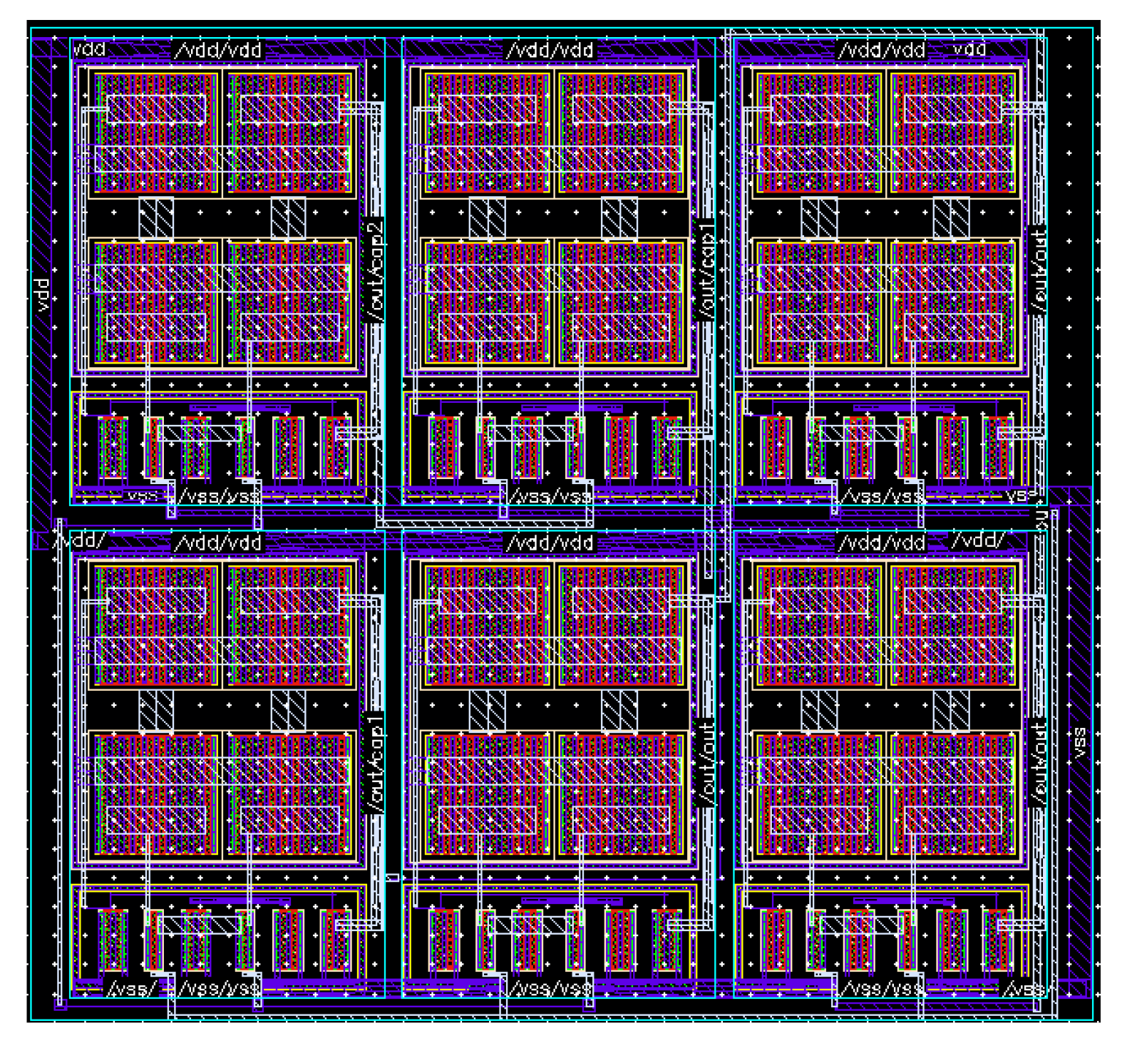
4. Implementations of the Power-Law Bilinear Negative Group Delay Filters
Let us consider power-law bilinear filters with ,  rad/s, and . With regards to the limitations, we might encounter when considering non-integer systems in integer-order, the only one is derived by the trade-off between the circuit complexity and the level of accuracy. Employing a second-order curve-fitting-based approximation in the range  rad/s, the obtained gain and group delay responses for each case are given by the plots in Figure 3. The values of the  and  are {3.19 rad/s, 270 ms}, {1.99 rad/s, 375 ms} and {1.63 rad/s, 440 ms}, respectively, with ideal values being {3.1 rad/s, 269 ms}, {1.99 rad/s, 375 ms} and {1.63 rad/s, 440 ms}.
      
    
    Figure 3.
      Approximated gain and group delay responses of power-law bilinear filters with ,  rad/s and .
  
Therefore, the employment of this approximation order is sufficient for achieving high accuracy, and the resulting rational integer-order transfer function can be expressed in a standard filter form as


      where  are the frequency and quality factor of the poles, and  are real scaling factors.
In general, this transfer function can be implemented through the following procedures:
- (a)
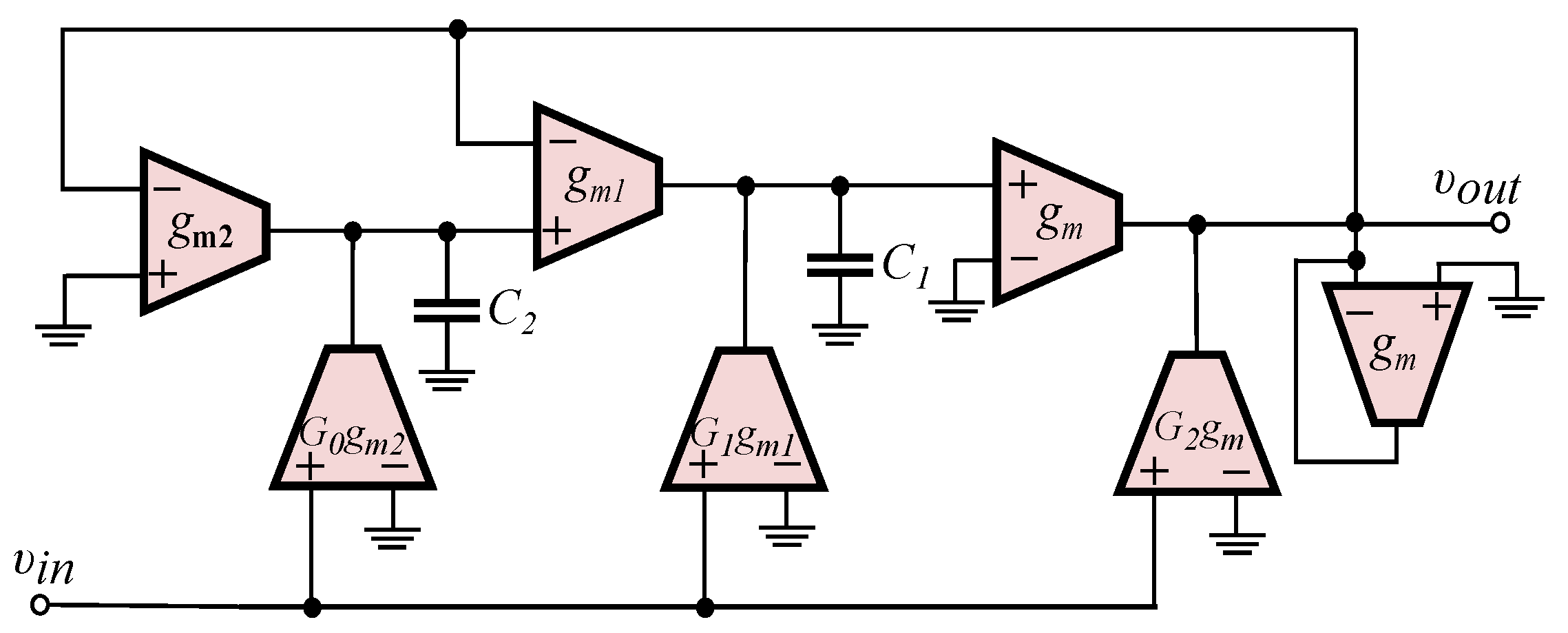
 - Employing the functional block diagram of a multi-feedback topology, e.g., the Inverse-Follow-the-Leader Feedback (IFLF), and using suitable active elements that offer electronic adjustment of the required time constants and scaling factors [].Choosing Operational Transconductance Amplifiers (OTAs) as active elements, the resulting structure is depicted in Figure 4, with the realized transfer function being
 - (b)
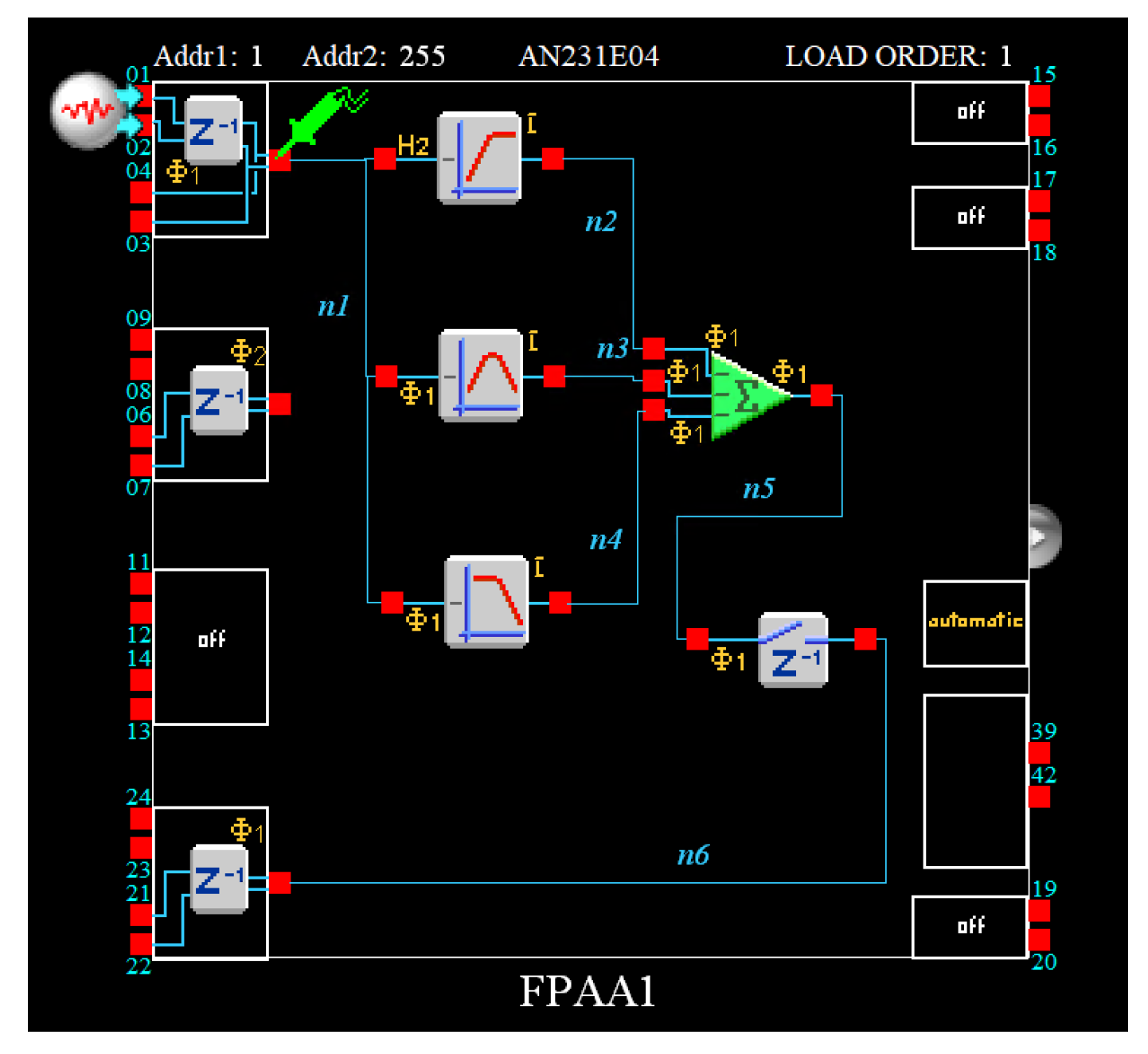
 - Employing a Field Programmable Analog Array (FPAA) device, such as the Anadigm AN231E04 device [,], where programmability is achieved through the utilization of the switched-capacitor technique. For this purpose, the transfer function in (26) is alternatively expressed as a sum of high-pass, band-pass, and low-pass biquad filters
 - (c)
 - Employing the concept in [], the transfer function in (26) is expressed as a ratio of two impedances, i.e., . According to [], the choice of the impedances depends on the transfer function that will be realized. Additionally, in order for the impedance to be realizable by a Cauer or Foster network, its frequency response must have the form of a low-pass filter. Inspecting the gain responses in Figure 3, it is obtained that the response of the filter has the form of an inverse high-pass filter in the range of interest. Therefore, the impedance will be implemented by a Cauer/Foster network, and will be equal to , while , with being an ohmic resistor with an arbitrary value. The resulting scheme is demonstrated in Figure 6, where the Cauer type-I network is utilized for implementing the impedance . The corresponding design equations are summarized in (30) as,where are the coefficients of the continued fraction expansion of the transfer function [].


    Figure 4.
      OTA-C implementation of the transfer function in (26).


    Figure 5.
      FPAA based implementation of the transfer function in (26).


    Figure 6.
      Implementation of (26) using a CFOA as the active element and a Cauer type-I RC network.
  
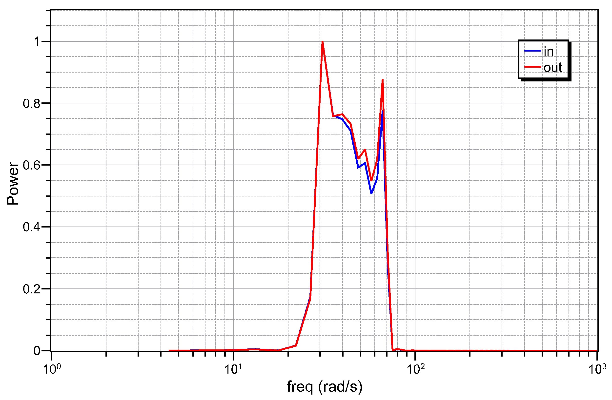
5. Simulation and Experimental Results
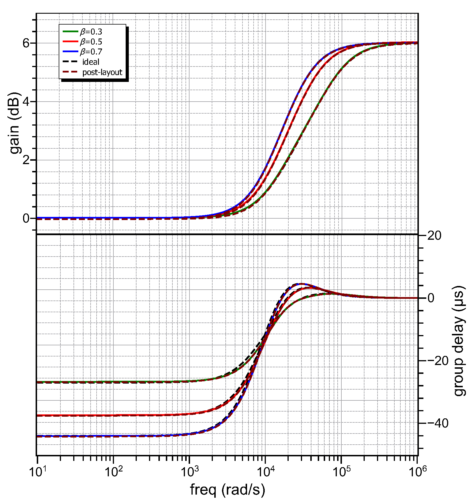
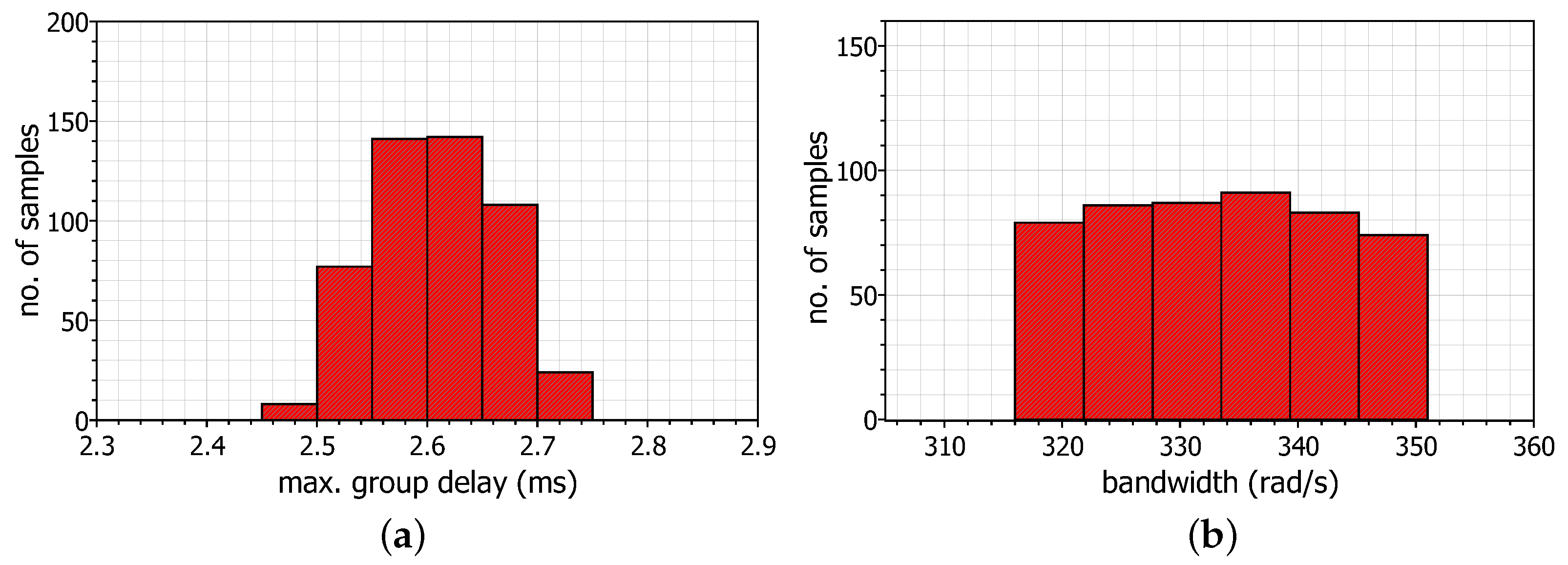
5.1. Simulation Results
The implementation of Figure 4 is achieved employing the OTA circuitry in Figure 7 []. The MOS transistors are biased in the strong inversion region, so their transconductance will be calculated using the following equation , where the gain factor of the nMOS transistor is defined as: , with  being the charge carrier mobility, and  the gate oxide capacitance per unit area. The parameters  and W/L represent the bias current and the aspect ratio of the transistor, respectively. As the transconductance parameter of the OTA is an adjustable variable determined by the bias current, the frequency characteristics of the filter can be electronically tuned. The behavior of the power-law bilinear filters is evaluated using the design kit provided by the Austria Mikro Systeme (AMS) CMOS 0.35 μm process. Considering that  krad/s, and , and power supply voltages  V, the appropriate MOS transistors aspect ratios chosen are 20 μm/1 μm for Mb1–Mb4, 10 μm/1 μm for Mn1–Mn2, and 200 μm/1 μm for Mp1–Mp4. According to (28), for  = 1 nF and  = 5 nF, the values of transconductances of the OTAs, as well as of the scaling factors and of the bias currents are summarized in Table 2, for each order. The summation stage has a bias current equal to 22 μA and transconductance 130 μS in all cases. Moreover, as the scaling factor  is always equal to 1 in this design, this stage could be omitted, simplifying the overall circuit.
      
    
    Figure 7.
      OTA circuitry. [].


    Table 2.
    Values of transconductances of the OTAs and of the scaling factors and bias currents.
  
The layout design of the active core of the filters is depicted in Figure 8 and the post-layout gain and group delay responses are presented in Figure 9, along with the corresponding theoretical responses with black dashed lines. The simulated maximum group delay values  for the power-law bilinear filters are 26.73 μs, 37.4 μs and 44.05 μs, close to the theoretical ones 27.02 μs, 37.5 μs and 43.99 μs, respectively, for the orders  = 0.3, 0.5, 0.7. The associated bandwidths are 31.49 krad/s, 19.99 krad/s and 16.36 krad/s, which are close to the theoretically predicted 31.59 krad/s, 19.9 krad/s and 16.35 krad/s.
      
    
    Figure 8.
      Layout design of the active core of the power-law bilinear filters (the area is 183.1 m × 171.4 m).


    Figure 9.
      Post-layout gain and group delay responses of power-law bilinear filters with  = 0.3, 0.5, 0.7 realized by the topology in Figure 4.
  
The sensitivity of the designed power-law bilinear filters has been evaluated through the Monte-Carlo analysis tool offered by the Analog Design Environment tool of the Cadence IC design suite in the case of . The resulting statistical plots for 500 runs are depicted in Figure 10, where the standard deviation for the maximum group delay is 4.99 μs and for the bandwidth 0.7 krad/s. Compared with the corresponding mean values 26.73 μs and 31.49 krad/s, the filters robustness is confirmed.
      
    
    Figure 10.
      Monte-Carlo analysis results concerning (a) the maximum group delay, and (b) the bandwidth, realized by the topology in Figure 4 for .
  
The time-domain behavior of the filters is performed using as stimulus a Sync signal and the obtained input and output waveforms are demonstrated in Figure 11. The measured delays between the peaks of the envelop of the output signals and the input signal are −24.24 μs, −23.54 μs and −24.87 μs for  = 0.3, 0.5, 0.7, which closely match the theoretical value of −25.63 μs, confirming their accuracy.
      
    
    Figure 11.
      Time-domain waveforms of the topology in Figure 6, stimulated by a Sync signal.
  
Assuming  rad/s, and the range of approximation () rad/s, and  = 10 k, the passive elements values (rounded to the E96 series defined in IEC 60063 standard) of Cauer type-I network, are summarized in Table 3. Utilizing OrCAD PSpice, with the AD844 discrete component biased at ±10 V employed as CFOA [], the simulated gain and group delay responses of the power-law bilinear filters are depicted in Figure 12, with the associated theoretical responses represented by black dashed lines. The maximum group delay values  for the power-law bilinear filters are 2.61 ms, 3.69 ms and 4.4 ms, close to the theoretical ones 2.7 ms, 3.7 ms and 4.4 ms, respectively, for the orders  = 0.3, 0.5, 0.7. The associated bandwidths are 332.5 rad/s, 206.6 rad/s and 168.4 rad/s, which are close to those predicted by the theory, 315.9 rad/s, 199.2 rad/s and 163.5 rad/s.
       
    
    Table 3.
    Values of the RC Cauer-I network for implementing the power-law bilinear filters of orders .


    Figure 12.
      Simulated gain and group delay responses of power-law bilinear filters with  realized by the topology in Figure 6.
  
The sensitivity analysis is performed by employing the Monte-Carlo analysis, offered by the Advanced Analysis tool of the OrCAD PSpice for the case of the power-law bilinear filter of order . The statistical plots (for N = 500 runs) of the maximum group delay and bandwidth are demonstrated in Figure 13. The values of the standard deviation are 56.3 s for the maximum group delay and 9.73 rad/s for the bandwidth, which are derived by considering  deviation from the nominal values of passive elements. Given that the mean values are 2.61 ms and 332.5 rad/s, this confirms the filter’s reasonable sensitivity characteristics.
      
    
    Figure 13.
      Monte-Carlo analysis results for (a) the maximum group delay, and (b) the bandwidth, realized by the topology in Figure 6 for .
  
The time-domain behavior of the topologies under consideration is evaluated by using as stimulus an electrocardiogram (ECG) signal. The resulting output waveforms are depicted in Figure 14, where the measured delays between the peaks of the envelope of the output signals and the input signal are −2.77 ms, −2.77 ms and −5.55 ms, which closely match the theoretical values of −2.8 ms, −2.8 ms and −5.5 ms, respectively, for . The effect of the filter on the spectrum of the input ECG signal is depicted in Figure 15, where it the evident that the spectrum of the resulting output signal is slightly modified due to the non-constant gain within the bandwidth of the ECG signal.
      
    
    Figure 14.
      Time-domain input and output waveforms of the topology in Figure 6, stimulated by an ECG signal.


    Figure 15.
      Effect of the filter on the spectrum of the input ECG signal for .
  
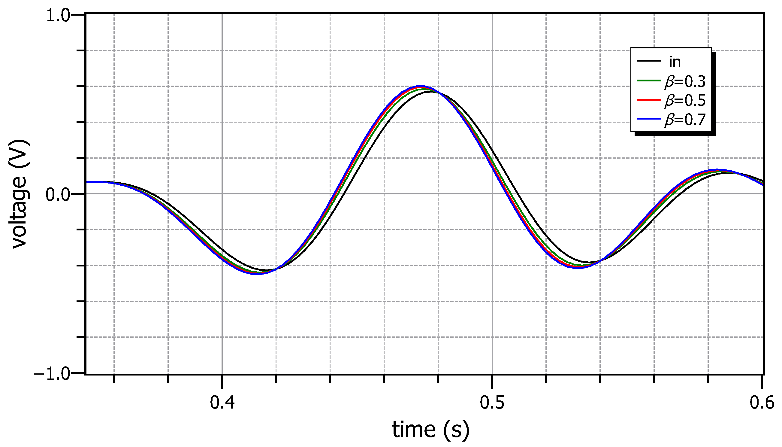
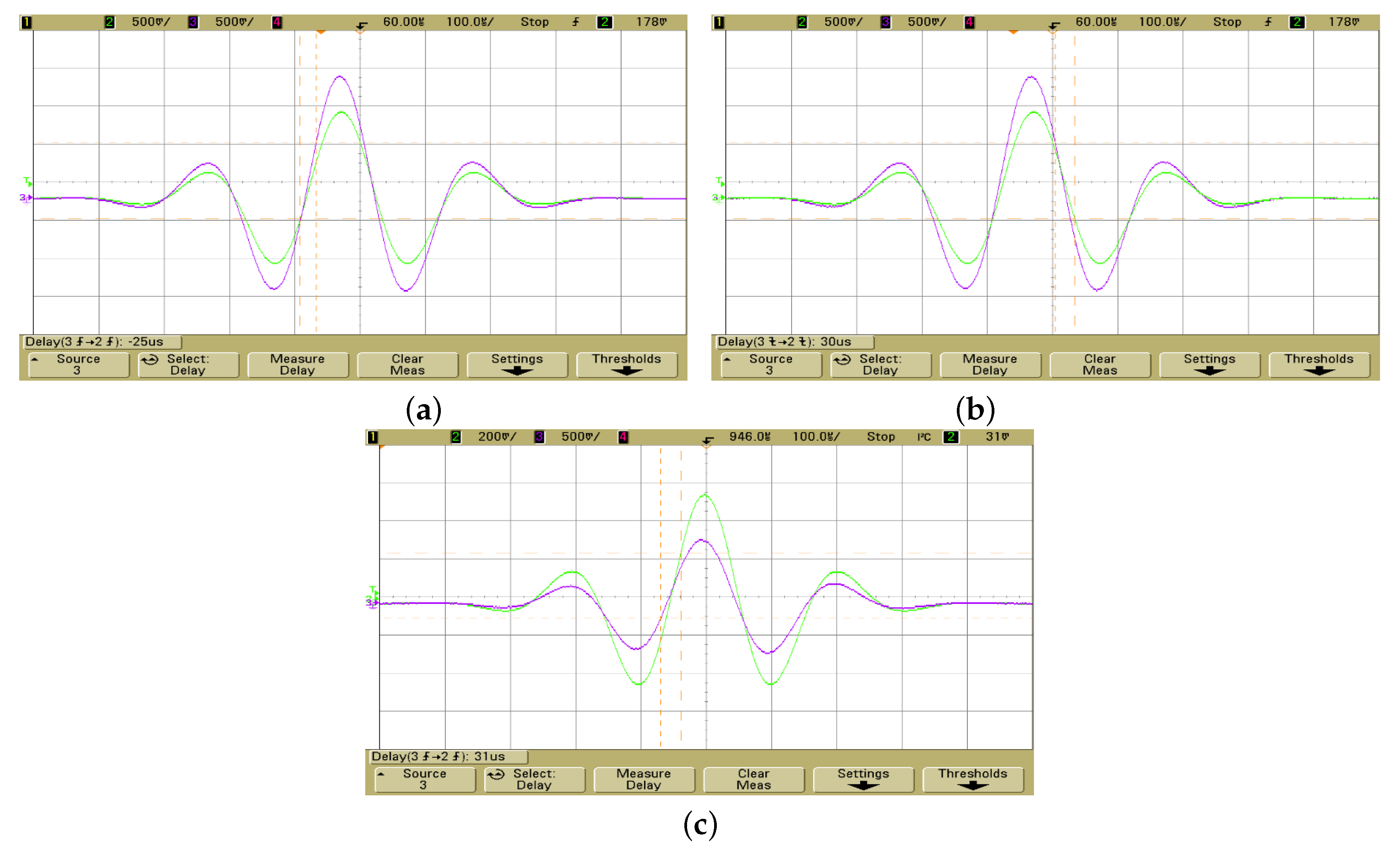
5.2. Experimental Results
The experimental verification of the power-law bilinear filters is presented where the design in Figure 5 is employed with clock frequency 500 kHz. Using the Keysight IntuiLink Waveform Editor for Function/Arbitrary Waveform Generators® a Gaussian pulse of 1 kHz frequency is used as stimulus signal for the FPAA device, through an Agilent 33250A arbitrary waveform generator. The associated screenshots, containing the input and output waveforms, obtained through the employment of an Agilent DSO6034A oscilloscope, are provided in Figure 16. The measured delays between the peaks of the envelop of the output and input signals are −25 μs, −30 μs and −31 μs, close to the corresponding values −23.2 μs, −31.1 μs and −35.3 μs, which are derived from the theory.
      
    
    Figure 16.
      Screenshot from the Agilent DSO 6034A oscilloscope about the input (green) and output (magenta) waveforms realized by the FPAA device, stimulated by a Gaussian pulse for (a)  (b) , and (c) .
  
6. Conclusions
The comparison between integer-order and power-law filters shows that, in terms of the product of the bandwidth and the maximum achievable group delay, the power-law bilinear filters are beneficial with regards to their integer-order counterparts. The involved implementation strategies, including curve-fitting approximations, multi-feedback topologies, and a Field Programmable Analog Array (FPAA) device, showcase the versatility and adaptability of the proposed filters. Simulations were performed over a broad frequency range, validating the accuracy of the designed filters, while experimental results, obtained using Anadigm AN231E04 FPAA platforms, provided real-world validation of our proposed designs. The achieved performance closely aligned with the simulation predictions, confirming the feasibility and reliability of the proposed power-law bilinear NGD filter designs. In conclusion, the presented designs offer enhanced performance characteristics, making them suitable for applications where precise control over group delay and bandwidth is crucial.
Author Contributions
Conceptualization, C.P., J.N., A.S.E. and B.J.M.; methodology, J.N. and C.P.; software, J.N.; validation, J.N.; formal analysis, J.N.; investigation, J.N. and C.P.; writing—original draft preparation, C.P.; writing—review and editing, C.P., A.S.E. and B.J.M.; project administration, C.P., A.S.E. and B.J.M. All authors have read and agreed to the published version of the manuscript.
Funding
This research received no external funding.
Institutional Review Board Statement
Not applicable.
Informed Consent Statement
Not applicable.
Data Availability Statement
Data are contained within the article.
Conflicts of Interest
The authors declare no conflicts of interest.
Abbreviations
The following abbreviations are used in this manuscript:
      
| AMS | Austria Mikro Systeme | 
| CAMs | Configured Analog Modules | 
| CFOA | Current Feedback Operational Amplifier | 
| CMOS | Complimentary Metal-Oxide Semiconductor | 
| ECG | Electrocardiogram | 
| FO | Fractional-Order | 
| FPAA | Field Programmable Analog Array | 
| IC | Integrated Circuit | 
| IFLF | Inverse-Follow-the-Leader-Feedback | 
| LHP | Left Half-Plane | 
| MOS | Metal-Oxide Semiconductor | 
| NGD | Negative Group Delay | 
| OTA | Operational Transconductance Amplifier | 
| RF | Radio Frequency | 
| RC | Resistor Capacitor | 
References
- Mitchell, M.W.; Chiao, R.Y. Negative group delay and ’fronts’ in a causal system: An experiment with very low frequency bandpass amplifiers. Phys. Lett. A 1997, 230, 133–138. [Google Scholar] [CrossRef]
 - Mitchell, M.W.; Chiao, R.Y. Causality and negative group delays in a simple bandpass amplifier. Am. J. Phys. 1998, 66, 14–19. [Google Scholar] [CrossRef]
 - Solli, D.; Chiao, R.; Hickmann, J. Superluminal effects and negative group delays in electronics, and their applications. Phys. Rev. E 2002, 66, 056601. [Google Scholar] [CrossRef]
 - Kitano, M.; Nakanishi, T.; Sugiyama, K. Negative group delay and superluminal propagation: An electronic circuit approach. IEEE J. Sel. Top. Quantum Electron. 2003, 9, 43–51. [Google Scholar] [CrossRef]
 - Munday, J.; Henderson, R. Superluminal time advance of a complex audio signal. Appl. Phys. Lett. 2004, 85, 503–505. [Google Scholar] [CrossRef]
 - Voss, H.U.; Stepp, N. A negative group delay model for feedback-delayed manual tracking performance. J. Comput. Neurosci. 2016, 41, 295–304. [Google Scholar] [CrossRef]
 - Voss, H.U. A delayed-feedback filter with negative group delay. Chaos Interdiscip. J. Nonlinear Sci. 2018, 28, 113113. [Google Scholar] [CrossRef] [PubMed]
 - Pyragiene, T.; Pyragas, K. Design of a negative group delay filter via reservoir computing approach: Real-time prediction of chaotic signals. Phys. Lett. A 2019, 383, 3088–3094. [Google Scholar] [CrossRef]
 - Wan, F.; Miao, X.; Ravelo, B.; Yuan, Q.; Cheng, J.; Ji, Q.; Ge, J. Design of multi-scale negative group delay circuit for sensors signal time-delay cancellation. IEEE Sens. J. 2019, 19, 8951–8962. [Google Scholar] [CrossRef]
 - Pyragiene, T.; Pyragas, K. Anticipatory synchronization via low-dimensional filters. Phys. Lett. A 2017, 381, 1893–1898. [Google Scholar] [CrossRef]
 - Wan, F.; Yuan, Z.; Ravelo, B.; Ge, J.; Rahajandraibe, W. Low-pass NGD voice signal sensoring with passive circuit. IEEE Sens. J. 2020, 20, 6762–6775. [Google Scholar] [CrossRef]
 - Chou, P.Y.; Chien, J.F.; Chen, K.S.; Huang, Y.T.; Chen, C.C.; Chan, C. Anticipation and negative group delay in a retina. Phys. Rev. E 2021, 103, L020401. [Google Scholar] [CrossRef]
 - Baloglu, O.; Cicekoglu, O.; Herencsar, N. OTA-C signal delay compensation circuit for transimpedance-mode audio signal processing systems. Integration 2023, 90, 205–213. [Google Scholar] [CrossRef]
 - Baloglu, O.; Cicekoglu, O.; Herencsar, N. Single CFOA-based active Negative Group Delay circuits for signal anticipation. Eng. Sci. Technol. Int. J. 2023, 48, 101590. [Google Scholar] [CrossRef]
 - Ravelo, B.; Pérennec, A.; Le Roy, M.; Boucher, Y.G. Active microwave circuit with negative group delay. IEEE Microw. Wirel. Components Lett. 2007, 17, 861–863. [Google Scholar] [CrossRef]
 - Ravelo, B. Synthesis of RF circuits with negative time delay by using LNA. Adv. Electromagn. 2013, 2, 44–54. [Google Scholar] [CrossRef]
 - Ravelo, B. Similitude between the NGD function and filter gain behaviours. Int. J. Circuit Theory Appl. 2014, 42, 1016–1032. [Google Scholar] [CrossRef]
 - Xiao, J.K.; Wang, Q.F.; Ma, J.G. Negative group delay circuits and applications: Feedforward amplifiers, phased-array antennas, constant phase shifters, non-foster elements, interconnection equalization, and power dividers. IEEE Microw. Mag. 2021, 22, 16–32. [Google Scholar] [CrossRef]
 - Wan, F.; Gu, T.; Li, B.; Li, B.; Rahajandraibe, W.; Guerin, M.; Lalléchère, S.; Ravelo, B. Design and Experimentation of Inductorless Low-Pass NGD Integrated Circuit in 180-nm CMOS Technology. IEEE Transcations Comput. Aided Des. Integr. Circuits Syst. 2022, 41, 4965–4974. [Google Scholar] [CrossRef]
 - Ravelo, B.; Bilal, H.; Rakotonandrasana, S.; Guerin, M.; Haddad, F.; Ngoho, S.; Rahajandraibe, W. Transient Characterization of New Low-Pass Negative Group Delay RC-Network. IEEE Trans. Circuits Syst. II Express Briefs 2024, 71, 126–130. [Google Scholar] [CrossRef]
 - Nakanishi, T.; Sugiyama, K.; Kitano, M. Demonstration of negative group delays in a simple electronic circuit. Am. J. Phys. 2002, 70, 1117–1121. [Google Scholar] [CrossRef]
 - Ravelo, B. Methodology of elementary negative group delay active topologies identification. IET Circuits Devices Syst. 2013, 7, 105–113. [Google Scholar] [CrossRef]
 - Ravelo, B. First-order low-pass negative group delay passive topology. Electron. Lett. 2016, 52, 124–126. [Google Scholar] [CrossRef]
 - Abuelmaatti, M.T.; Khalifa, Z.J. A new CFOA-based negative group delay cascadable circuit. Analog Integr. Circuits Signal Process. 2018, 95, 351–355. [Google Scholar] [CrossRef]
 - Wan, F.; Wang, L.; Ji, Q.; Ravelo, B. Canonical transfer function of band-pass NGD circuit. IET Circuits Devices Syst. 2019, 13, 125–130. [Google Scholar] [CrossRef]
 - Randriatsiferana, R.; Gan, Y.; Wan, F.; Rahajandraibe, W.; Vauché, R.; Murad, N.M.; Ravelo, B. Study and experimentation of a 6-dB attenuation low-pass NGD circuit. Analog. Integr. Circuits Signal Process. 2022, 110, 105–114. [Google Scholar] [CrossRef]
 - Yuan, A.; Fang, S.; Wang, Z.; Liu, H. A novel multifunctional negative group delay circuit for realizing band-pass, high-pass and low-pass. Electronics 2021, 10, 1742. [Google Scholar] [CrossRef]
 - Maundy, B.; Elwakil, A.; Psychalinos, C. Systematic design of negative group delay circuits. AEU Int. J. Electron. Commun. 2024, 174, 155060. [Google Scholar] [CrossRef]
 - Banchuin, R. On the fractional domain analysis of negative group delay circuits. Int. J. Circuit Theory Appl. 2023; in press. [Google Scholar] [CrossRef]
 - Kapoulea, S.; Psychalinos, C.; Elwakil, A.S. Power law filters: A new class of fractional-order filters without a fractional-order Laplacian operator. AEU-Int. J. Electron. Commun. 2021, 129, 153537. [Google Scholar] [CrossRef]
 - Nako, J.; Psychalinos, C.; Elwakil, A.S. One active element implementation of fractional-order Butterworth and Chebyshev filters. AEU-Int. J. Electron. Commun. 2023, 168, 154724. [Google Scholar] [CrossRef]
 - Tsirimokou, G.; Psychalinos, C.; Elwakil, A. Design of CMOS Analog Integrated Fractional-Order Circuits: Applications in Medicine and Biology; Springer: Berlin/Heidelberg, Germany, 2017. [Google Scholar] [CrossRef]
 - Shen, H.; Wang, Z. A Circuit Principle and Simulation Test for Negative Group Delay. Int. J. Adv. Netw. Monit. Control. 2022, 7, 46–57. [Google Scholar] [CrossRef]
 - Nako, J.; Psychalinos, C.; Elwakil, A.S.; Minaei, S. Non-Integer Order Generalized Filters Designs. IEEE Access 2023, 11, 116846–116859. [Google Scholar] [CrossRef]
 - Anadigm. AN231E04 dpASP: The AN231E04 dpASP Dynamically Reconfigurable Analog Signal Processor. Available online: https://www.anadigm.com (accessed on 4 December 2023).
 - Hassanein, A.M.; Madian, A.H.; Radwan, A.G.; Said, L.A. On the Design Flow of the Fractional-Order Analog Filters between FPAA Implementation and Circuit Realization. IEEE Access 2023, 11, 29199–29214. [Google Scholar] [CrossRef]
 - Nako, J.; Psychalinos, C.; Elwakil, A.S. A 1 + α Order Generalized Butterworth Filter Structure and Its Field Programmable Analog Array Implementation. Electronics 2023, 12, 1225. [Google Scholar] [CrossRef]
 - Tsirimokou, G. A systematic procedure for deriving RC networks of fractional-order elements emulators using MATLAB. AEU-Int. J. Electron. Commun. 2017, 78, 7–14. [Google Scholar] [CrossRef]
 - Analog Devices. AD844 60 MHz 2000 V/us Monolithic Op Amp with Quad Low Noise, Data Sheet, rev. G. Available online: https://www.analog.com/en/products/ad844.html (accessed on 26 November 2023).
 
Disclaimer/Publisher’s Note: The statements, opinions and data contained in all publications are solely those of the individual author(s) and contributor(s) and not of MDPI and/or the editor(s). MDPI and/or the editor(s) disclaim responsibility for any injury to people or property resulting from any ideas, methods, instructions or products referred to in the content.  | 
© 2024 by the authors. Licensee MDPI, Basel, Switzerland. This article is an open access article distributed under the terms and conditions of the Creative Commons Attribution (CC BY) license (https://creativecommons.org/licenses/by/4.0/).