Article

A 60 GHz Power Amplifier with Neutralization Capacitors and Compensation Inductors

1
Department of Semiconductor Convergence, Chungnam National University, Daejeon 34134, Republic of Korea
2
School of Electronics and Electrical Engineering, College of Engineering, Dankook University, Yongin-si 16890, Republic of Korea
*
Author to whom correspondence should be addressed.
Electronics 2024, 13(21), 4276; https://doi.org/10.3390/electronics13214276
Submission received: 1 October 2024 / Revised: 29 October 2024 / Accepted: 30 October 2024 / Published: 31 October 2024

Abstract

:
In this paper, we present a high power-added efficiency (PAE) and high gain per stage 60 GHz power amplifier (PA). The proposed PA consists of a two-stage common-source amplifier that incorporates neutralization capacitors and compensation inductors to enhance both gain and efficiency. The gain characteristics are analyzed, demonstrating that the proposed design improves both gain and efficiency. Implemented in 65 nm CMOS technology, the PA achieves a saturated output power of 13.4 dBm at 60 GHz, with a maximum PAE of 26.7% from a 1 V supply. The output 1 dB compression point is 10.5 dBm, with a PAE of 16%. The PA occupies a core chip area of 0.094 mm2.

1. Introduction

Recently, the unlicensed 60 GHz band has gained attention for its ability to transmit tens of gigabits per second of data due to its wide bandwidth [1,2,3]. In this frequency band, low-power, high-efficiency designs are critical for handheld device applications. Additionally, multiple-input multiple-output (MIMO) and phased array techniques have been introduced to enhance data rates and extend communication distances. However, these techniques require multiple transmitters and receivers, leading to increased power consumption, which makes their use in handheld devices challenging. In particular, power amplifiers (PAs) consume substantial DC power while offering limited efficiency.
As a key component, PAs with high power-added efficiency (PAE) and output power exceeding 13 dBm are essential for reducing battery consumption and extending the operating time of handheld devices. Thus, designing highly efficient PAs is a primary challenge for next-generation millimeter-wave (mm-wave) wireless systems. PA efficiency represents a significant bottleneck, especially in transmitter arrays. Over the past decade, significant progress has been made in developing high-power, high-efficiency PAs for mm-wave bands [4,5,6,7,8,9,10,11,12,13,14]. CMOS processes are widely used in mm-wave PA design due to their low cost and ability to integrate with digital baseband circuitry. Transformer-based common-source amplifiers are popular for their compact size and simple power matching and combining capabilities [7,8,9,10,11,12,13,14]. Most of the published CMOS PAs focused on achieving high output power by employing cascode topologies [8,9], power combining architectures [10,11,12], and linearity enhancement techniques [13]. Power combining techniques enable higher output power and gain [10,11,12], but this technique suffers from large chip areas and limited PAE. For instance, a PA with a two-way, four-stage common-source [10] achieved a saturated output power (PSAT) of 16 dBm, but with a PAE of only 17%. A 32-way, four-stage common-source PA [11] showed a gain of 21.9 dB and a PSAT of 24.1 dBm but required a large chip area and a huge power consumption. The linearized PA [13] achieved a PSAT of 15 dBm with a PAE of 26%, and an output 1 dB compression point (OP1dB) of 14 dBm with a PAE of 21%. However, this PA exhibited a limited gain of 14 dB due to the linearization technique. A variable gain PA [14] provides a variable gain of 23.5 dB, but requires multiple stages, limiting its PAE to 21.5%.
In this study, a high-efficiency 60 GHz PA was implemented for handheld devices such as smart phones, gaming consoles, augmented reality, and virtual reality devices. The proposed circuit uses a two-stage common-source amplifier with compensation inductors and neutralization capacitors to achieve high PAE and high gain per stage. As a result, the PA successfully achieved a power gain of 18.3 dB, an OP1dB of 10.5 dBm, and a peak PAE (PAEpeak) of 26.7% at 60 GHz. The measurement results indicate that the proposed PA is suitable for low-power mm-wave handheld devices.

2. Design Methodology

2.1. Active Device

The output power and efficiency of the PAs highly depend on active devices and parasitic components, as PAs typically utilize large transistors to achieve high output power. This issue becomes more pronounced in the mm-wave band, where operating frequencies approach the cut-off frequency and maximum oscillation frequency, leading to reductions in power gain and output power. Additionally, the parasitic capacitance of active devices further limits bandwidth, power gain, output power, and PAE. PAE can be expressed as
PAE = P OUT P IN P DC ,
where POUT, PIN, and PDC are the output power, input power, and power dissipation of the PA. PAE is a metric for rating the efficiency of the PA. To mitigate these challenges, careful design of transistor size and interconnections is essential.
To optimize the transistor size for the PA, we compared the performance of the power stage based on different device configurations. Table 1 presents the load-pull simulation results comparing transistors with one 4 μm × 25 fingers, two 2 μm × 25 fingers, and four 1 μm × 25 fingers in a differential common-source amplifier with neutralization capacitors [7]. All configurations maintain a total transistor width of 100 μm to achieve an output power above 13 dBm. The simulation results indicate that the configuration with two 2 μm × 25 fingers delivers superior PSAT and PAEpeak. As a result, we selected two 2 μm × 25 fingers for the power cell in the power stage of this design.
Figure 1a illustrates the proposed layout of the unit transistor cell for the drive and power stages. The unit cell employs transistors with a width of 2 μm and 25 fingers, occupying an area of 15 × 9 μm2. To optimize the layout, the source is connected using multiple metal layers (M4–M7) and linked to a double-sided ground plane (M1–M2). The M1 and gate poly are connected on both sides and routed to M8. Additionally, gate–source and gate–drain overlap is minimized to reduce parasitic capacitance. Figure 1b shows the layout of the two 2 μm × 25 fingers devices, which occupy an area of 28 × 9 μm2. The unit transistors are placed adjacent to each other, with the sources directly connected to minimize interconnection resistance. The gate and drain are routed through thick metal layers M8 and M9, respectively. In electromagnetic (EM) simulations, interconnection losses resulted in power gain degradations of 0.2 dB and 0.3 dB for the single 2 μm × 25 fingers and two 2 μm × 25 fingers transistors, respectively.

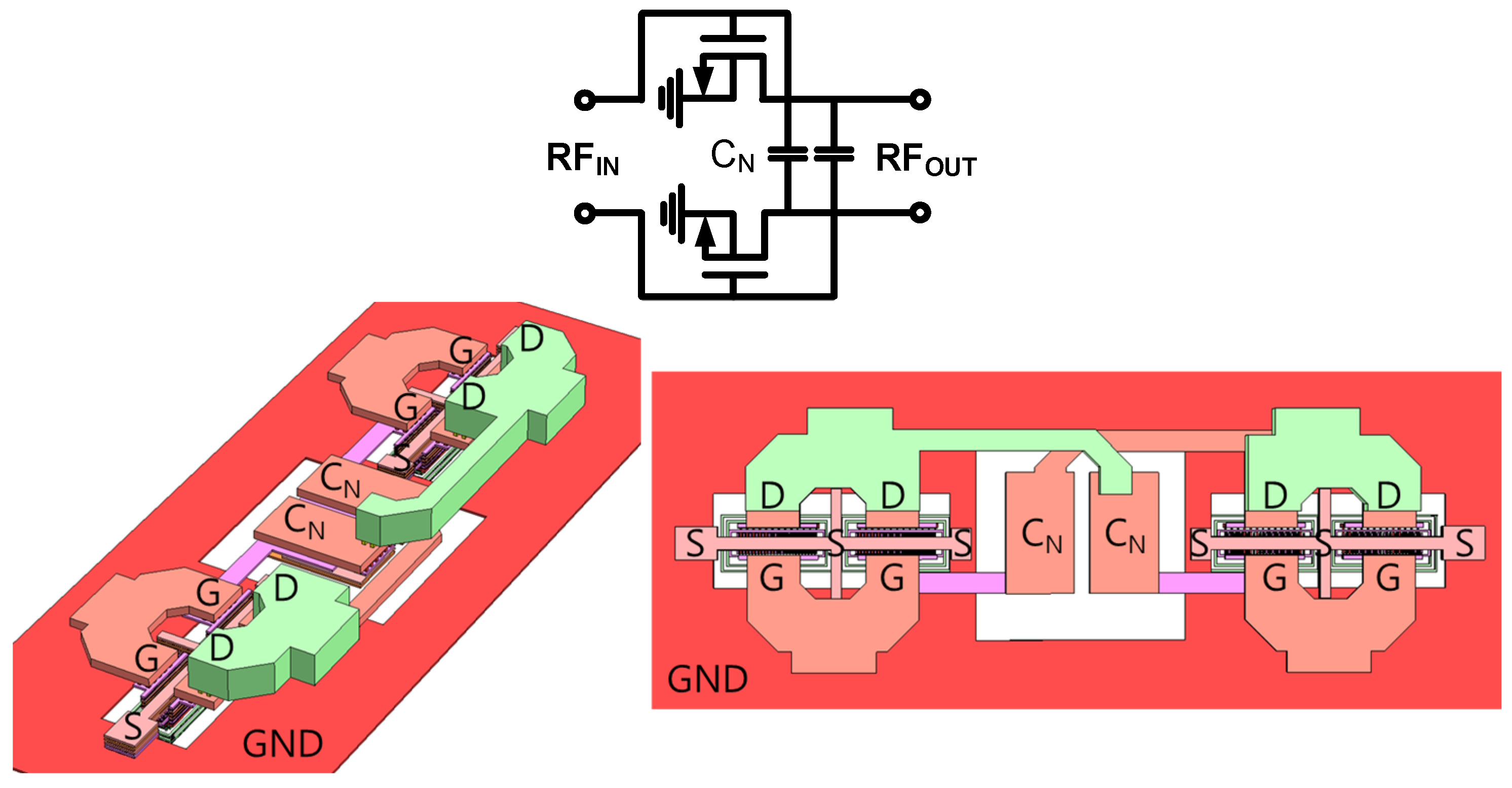
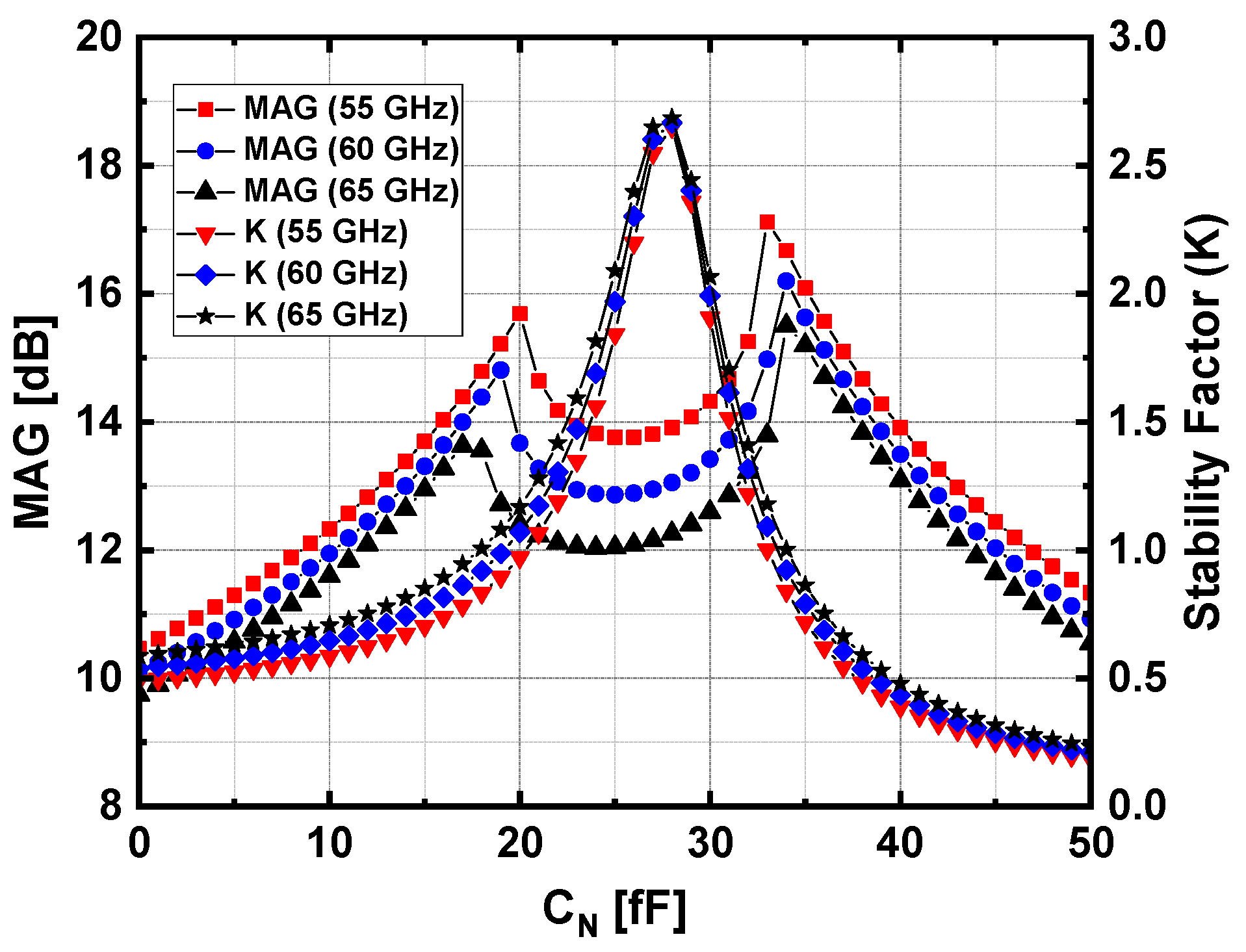
2.2. Neutralization Capacitors

In addition to optimizing transistor configuration and layout, neutralization capacitors [7] are employed to enhance gain and stability. Figure 2 shows the schematic and layout of the differential amplifier with neutralization capacitors for the power stage. The gate-to-drain parasitic capacitance, Cgd, creates a feedback path that degrades power gain, reverse isolation, and stability. The neutralization capacitors, CN, address these issues by neutralizing Cgd, effectively eliminating the feedback path.
The custom-designed metal–oxide–metal (MOM) capacitor [15] was used for CN, rather than the standard foundry-provided MOM capacitor. The custom MOM capacitor utilizes a multi-stack metal plate design for a smaller chip area, shorter interconnections, and sufficient vias to reduce parasitic resistance. Moreover, the custom MOM capacitor exhibited a minimal process variation of less than ±2%, compared to ±11% for the foundry-provided MOM capacitor, as shown in simulations.
Figure 3 illustrates the simulated maximum available gain (MAG) and stability factor of the differential common-source amplifier with the neutralization capacitor CN. The amplifier remains stable with up to ±20% variation in CN. A capacitance of 27 fF was selected for CN, slightly smaller than the required value for maximum stability, to account for additional parasitic capacitance. With the neutralization technique, the power stage achieves a MAG of 13.1 dB, an improvement of 3.0 dB compared to the design without neutralization. The neutralization capacitor is also applied to the driver stage to further enhance stability and gain.

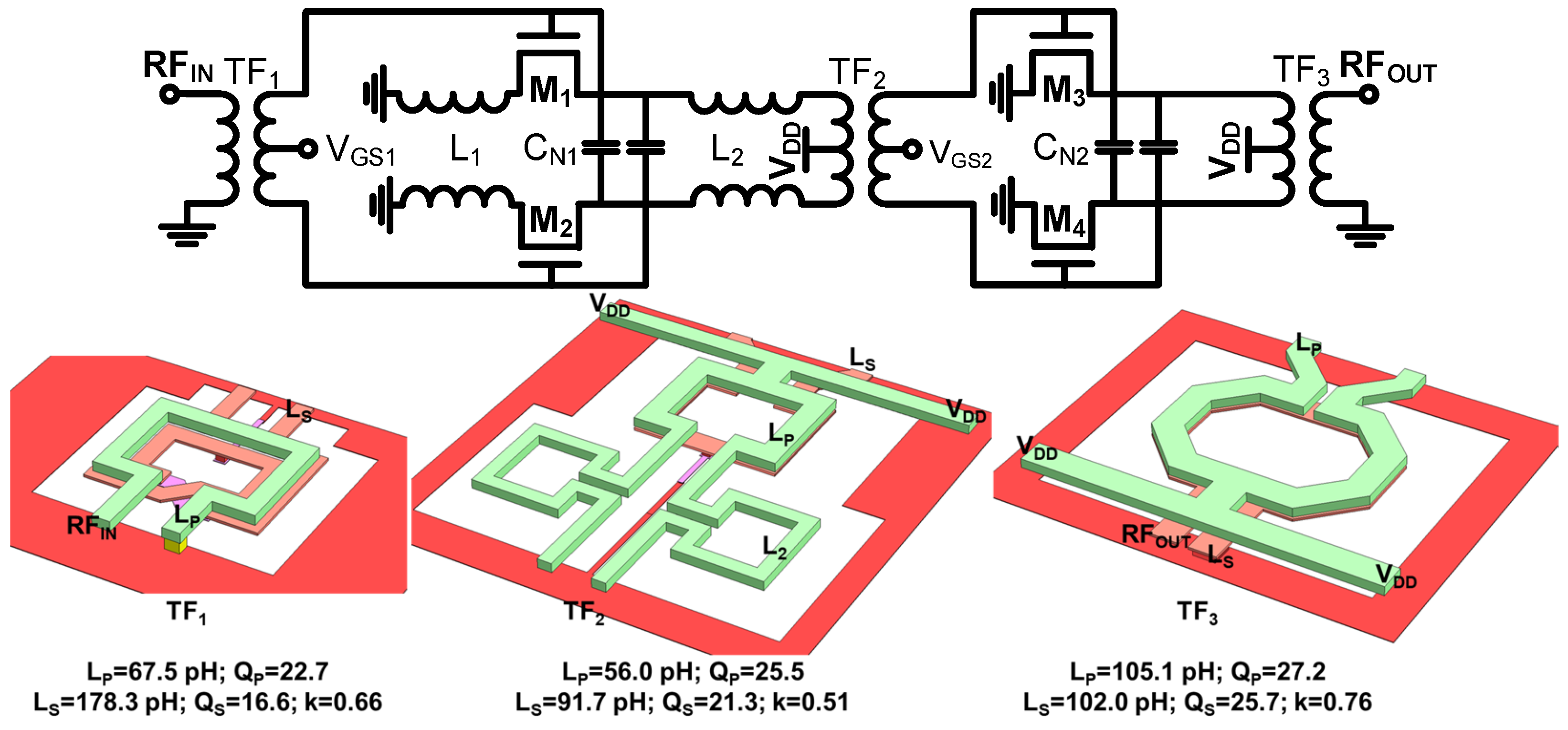
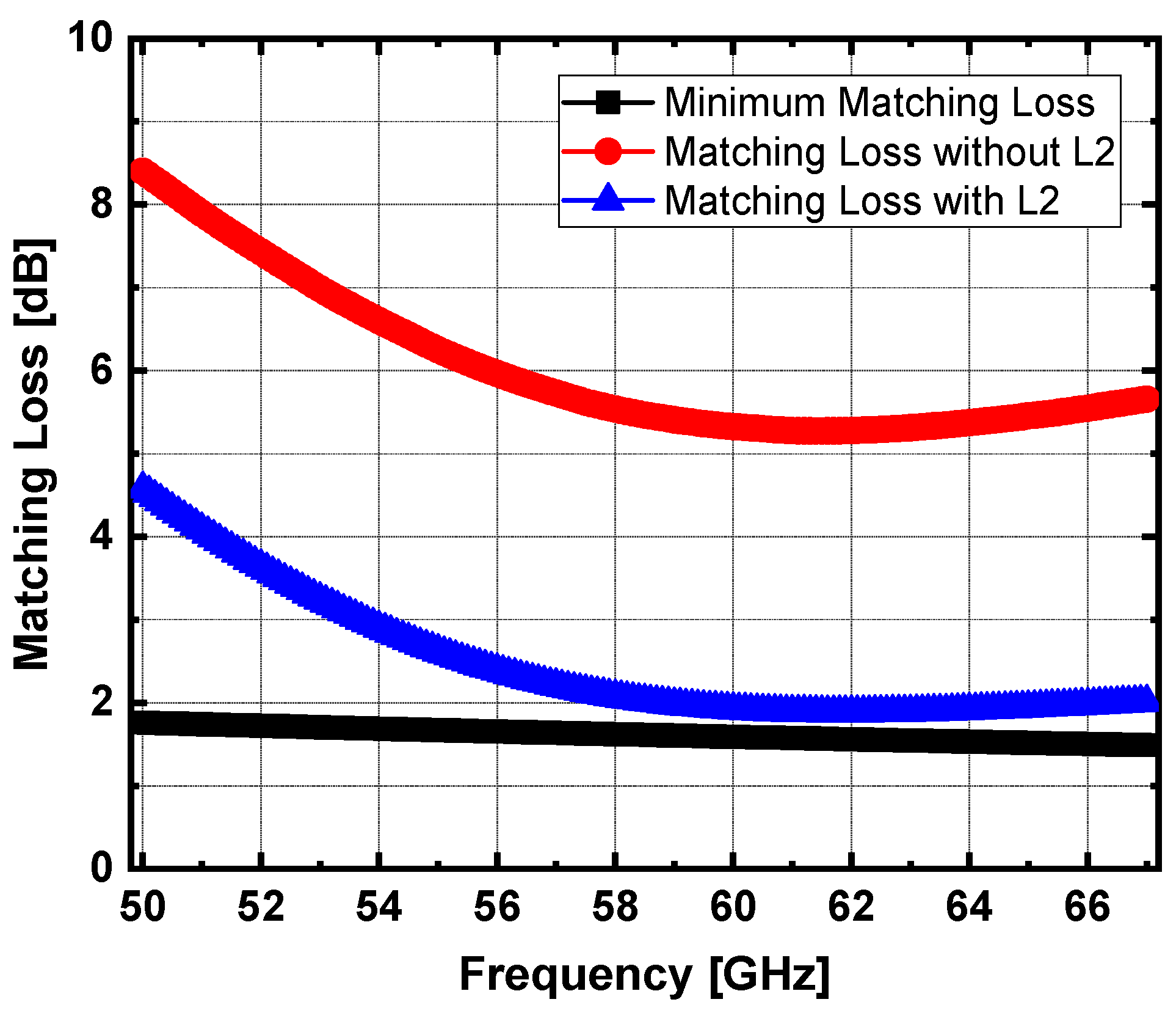
2.3. Proposed PA Design with Transformers and Compensation Inductors
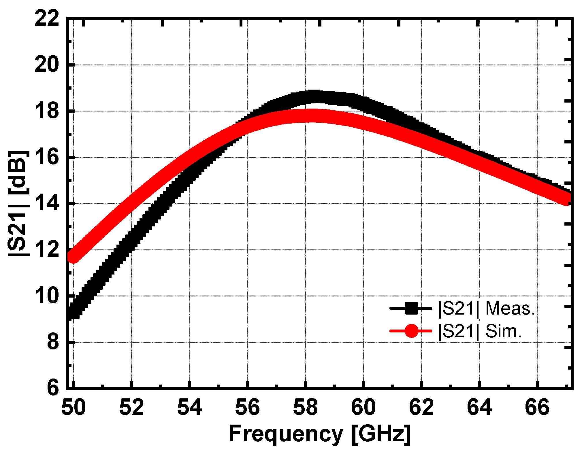
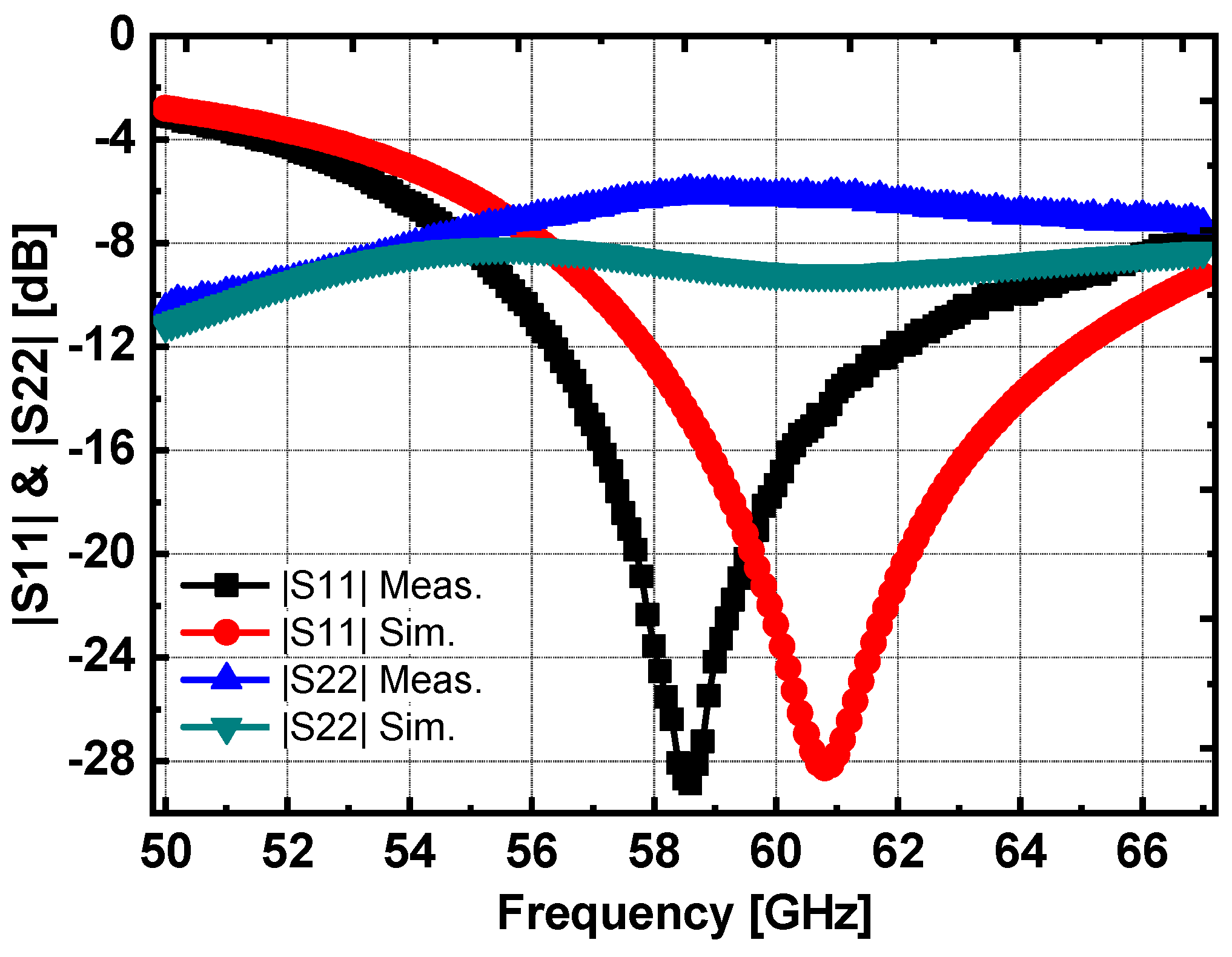
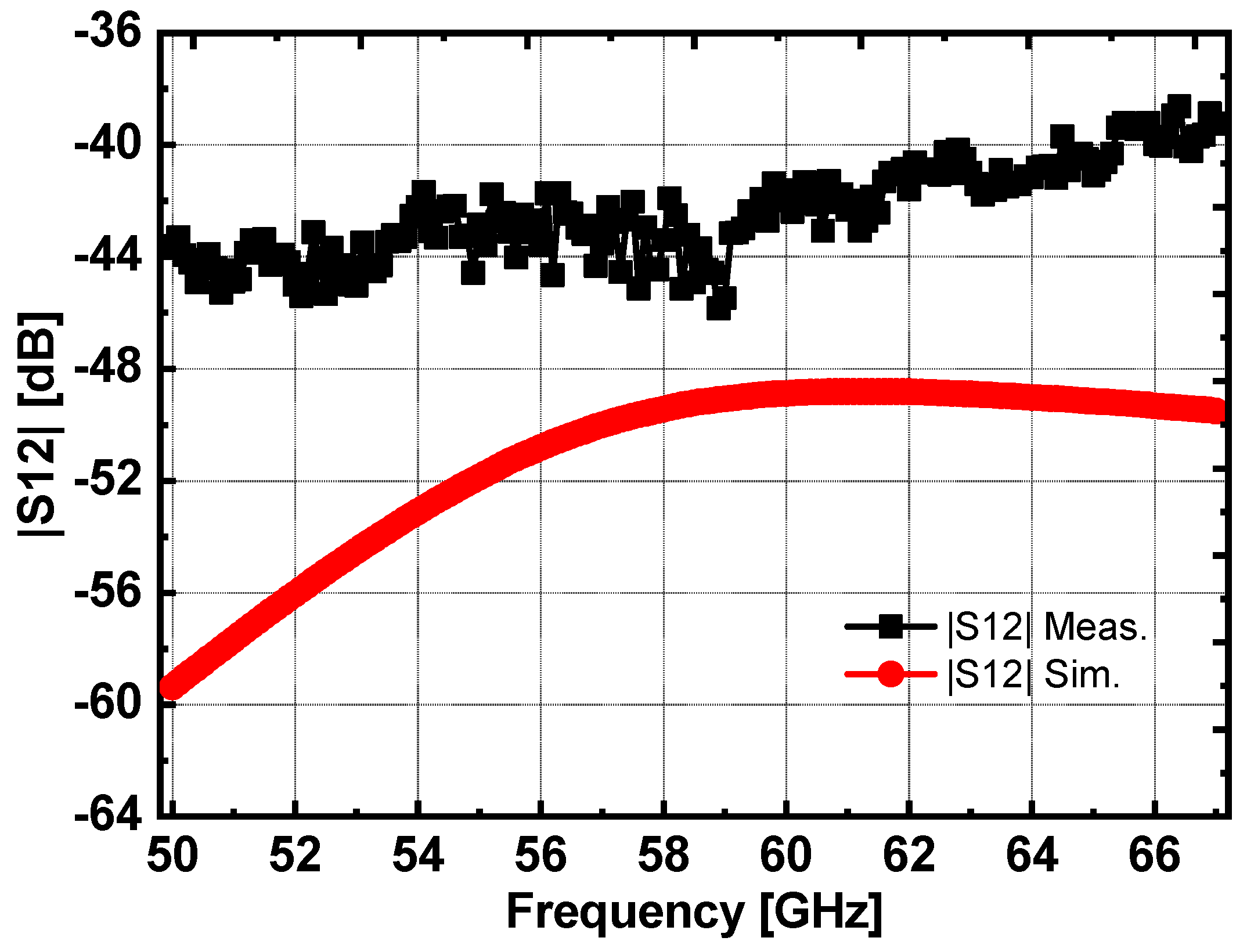
A simplified schematic of the proposed 60 GHz PA and the layout of the transformers are shown in Figure 4. The PA consists of a two-stage differential common-source amplifier with transformers, TF1–TF3, a matching network with compensation inductors, and neutralization capacitors, CN1 and CN2. The transistor size of the power stage is two times larger than that of the driver stage. The power stage has two 2 μm × 25 fingers devices, whereas the driver stage has a single 2 μm × 25 fingers device. In the power stage, two 2 μm × 25 fingers devices provide a better gain, PAE, and PSAT than a single 4 μm × 25 fingers device. The neutralization capacitors CN1 and CN2 are chosen to be 13.5 fF and 27 fF, respectively, for better power gain, isolation, and stability.
The first stage of the PA is implemented using a differential common-source amplifier with neutralization capacitors and inductive source degeneration. Inductor L1 is connected to the source terminals of the transistors M1 and M2, creating a series–series negative feedback loop. This feedback improves OP1dB and stability while slightly reducing power gain. The inductive source degeneration technique at the power stage also enhances the linearity, but the gain reduction at the second stage requires a higher linearity at the first stage. L1 is set to 24 pH to balance the improvement in OP1dB and stability with the reduction in gain. In the simulation, a 0.5 dB improvement in OP1dB is achieved, with a 1.5 dB reduction in gain, while the stability factor increases from 10 to 15 at 60 GHz.
A highly efficient matching network is crucial for enhancing gain, PAE, and PSAT. Transformer-based matching networks, paired with compensation inductors, are used to achieve high efficiency and a compact design. The transformers are implemented using two vertically coupled top metal layers. The input transformer balun TF1 has a turn ratio of 1:2 for impedance transformation. The output transformer TF3 is designed with a high coupling factor of 0.76, as the insertion loss of the transformer is proportional to the square of the coupling factor [16]. The inter-stage matching network uses compensation inductors L2 and a transformer, TF2, with a lower coupling coefficient and a 1:1 turn ratio. A coupling coefficient of 0.51 was selected for TF2 considering the matching loss and bandwidth. A lower coupling coefficient results in wider bandwidth but increases matching loss [4]. The compensation inductor L2 helps optimize the matching loss. As shown in Figure 5, the simulated inter-stage matching loss is 1.9 dB at 60 GHz. The inter-stage matching network, which combines the moderately coupled transformer TF2 with the compensation inductor L2, delivers high efficiency and gain by compensating the impedance mismatch between the driver-stage output and the power-stage input. Consequently, the matching loss of the inter-stage matching network with TF2 and L2 is 3.4 dB smaller than that with the transformer without a compensation inductor in the simulation.
A ground plane with a mesh pattern using the two bottom metal layers is used. The neutralization capacitors, inductors, interconnections, and transformers are all simulated using the HFSS 3-D EM simulator developed by Ansys, Canonsburg, PA, USA. The transistors, M1–M4, have a gate length of 60 nm. With the neutralization capacitors and compensation inductors, the proposed PA achieved a simulated gain of 17.6 dB, a simulated PSAT of 14 dBm, and a simulated PAEpeak of 26.5% at 60 GHz.

3. Results

The proposed PA circuit was implemented in a standard 65 nm CMOS technology. Figure 6 depicts a chip photograph of the proposed PA. The PA chip occupies an area of 0.58 × 0.46 mm2 including the bond pads and 0.094 mm2 excluding the pads. The PA dissipates a power of 58 mW from a 1 V supply voltage. Figure 7 illustrates measurement setups for the S-parameter and power handling capability. The S-parameter was measured with an E8361A vector network analyzer manufactured by Keysight, Santa Rosa, CA, USA and the results were calibrated using the Picoprobe SOLT (short–open–load–thru) GSG-67A calibration substrate. The large-signal measurements were performed with a signal generator, frequency multiplier, power sensor, and high-precision power meter. The measured losses of the probe tips, adapters, and coaxial cables were de-embedded from the raw measurement data.
Figure 8 shows the simulated and measured power gains of the 60 GHz PA. The measured gain of the proposed PA is 18.3 dB at 60 GHz. The measured peak gain is 18.7 dB at 58.3 GHz and the measured 3 dB bandwidth is 10.1 GHz (54.4–64.5 GHz). The difference between the simulated and measured data is probably due to the inaccuracy of the transistor model at 60 GHz, especially the drain-to-gate capacitance. Figure 9 depicts the simulated and measured input and output return losses of the proposed PA. The measured input and output return losses are larger than 8.4 dB and 6.0 dB, respectively, for 55.2–66 GHz. Figure 10 illustrates the simulated and measured reverse isolation of the proposed PA. The reverse isolation is smaller than −39 dB in the 60 GHz band.
Figure 11 shows the measured power gain, output power, and PAE. OP1dB and PSAT are 10.5 dBm and 13.4 dBm at 60 GHz, respectively. The maximum PAE is 26.7%. The measured PSAT is limited due to the limited input power of the signal generator and frequency multiplier. The neutralization capacitors and compensation inductors enhance the gain and PAE, which are suitable for low-power mm-wave handheld devices.

4. Discussion

Table 2 compares the performance of the state-of-the-art 60 GHz CMOS PAs. The proposed PA demonstrates high gain per stage and a high peak power-added efficiency (PAE). The PA in [8] achieves a high PAE, but it is implemented using 22 nm CMOS technology, which offers a significantly higher cut-off frequency and maximum oscillation frequency. The PA in [11] attains high output power, due to the use of larger transistors; however, this results in a substantial DC power consumption of 942 mW. The proposed PA utilized the neutralization capacitors and compensation inductors and enhanced the gain and PAE, which are suitable for low-power mm-wave handheld devices.

5. Conclusions

A 60 GHz PA circuit was implemented and designed using a standard 65 nm CMOS technology. The PA with neutralization capacitors and compensation inductors provides a gain of 18.3 dB with a maximum PAE of 26.7% at 60 GHz from a 1 V supply voltage. Furthermore, the PSAT is 13.4 dBm. The measurement results indicate that the proposed PA is suitable for application to low-power mm-wave handheld devices.

Author Contributions

Conceptualization, J.-H.K. and C.-W.B.; data curation, J.-H.K. and C.-W.B.; formal analysis, J.-H.K. and C.-W.B.; funding acquisition, C.-W.B.; investigation, C.-W.B.; methodology, J.-H.K. and C.-W.B.; project administration, C.-W.B.; resources, C.-W.B.; software J.-H.K. and C.-W.B.; supervision, C.-W.B.; validation, J.-H.K. and C.-W.B.; visualization, J.-H.K. and C.-W.B.; writing—original draft, J.-H.K.; writing—review and editing, J.-H.K. and C.-W.B. All authors have read and agreed to the published version of the manuscript.

Funding

The present research was supported by the research fund of Dankook University in 2023.

Data Availability Statement

Data are contained within this article.

Conflicts of Interest

The authors declare no conflicts of interest.

References

  1. Wang, Y.; Liu, B.; Wu, R.; Liu, H.; Narayanan, A.T. A 60-GHz 3.0-Gb/s Spectrum Efficient BPOOK Transceiver for Low-Power Short-Range Wireless in 65-nm CMOS. IEEE J. Solid-State Circuits 2019, 54, 1363–1374. [Google Scholar] [CrossRef]
  2. Byeon, C.W.; Eun, K.C.; Park, C.S. A 2.65-pJ/Bit 12.5-Gb/s 60-GHz OOK CMOS Transmitter and Receiver for Proximity Communications. IEEE Trans. Microw. Theory Tech. 2020, 68, 2902–2910. [Google Scholar] [CrossRef]
  3. Wang, Y.; Chung, H.; Ma, Q.; Rebeiz, G.M. A 57.5–65.5 GHz Phased-Array Transmit Beamformer in 45 nm CMOS SOI with 5 dBm and 6.1% Linear PAE for 400 MBaud 64-QAM Waveforms. IEEE Trans. Microw. Theory Tech. 2021, 69, 1772–1779. [Google Scholar] [CrossRef]
  4. Son, H.S.; Jang, T.H.; Kim, S.H.; Jung, K.P.; Kim, J.H.; Park, C.S. Pole-controlled wideband 120 GHz CMOS power amplifier for wireless chip-to-chip communication in 40-nm CMOS process. IEEE Trans. Circuits Syst. II Exp. Briefs 2019, 66, 1351–1355. [Google Scholar] [CrossRef]
  5. Kim, J. Broadband Millimeter-Wave Power Amplifier Using Modified 2D Distributed Power Combining. Electronics 2020, 9, 899. [Google Scholar] [CrossRef]
  6. Mayeda, J.; Lie, D.Y.C.; Lopez, J. Broadband Millimeter-Wave 5G Power Amplifier Design in 22 nm CMOS FD-SOI and 40 nm GaN HEMT. Electronics 2022, 11, 683. [Google Scholar] [CrossRef]
  7. Chan, W.L.; Long, J.R. A 58–65 GHz neutralized CMOS power amplifier with PAE above 10% at 1-V supply. IEEE J. Solid-State Circuits 2010, 45, 554–564. [Google Scholar] [CrossRef]
  8. Xu, X.; Wagner, J.; Ellinger, F. A 62-GHz High-Efficiency Power Amplifier with Modulation Capability via Back-Gate in 22-nm FD-SOI. IEEE Solid-State Circuits Lett. 2023, 6, 49–52. [Google Scholar] [CrossRef]
  9. Feng, J.; Lu, L.; Chen, X.; Sun, Y.; Wu, X.; Fan, X.; Li, L. A 60-GHz Variable-Gain Power Amplifier with a Switchable Inductor for TDD Systems. IEEE Microw. Wireless Tech. Lett. 2024, 34, 512–515. [Google Scholar] [CrossRef]
  10. Feng, J.; Liang, Y.; Niu, X.; Lu, L.; Chen, X.; Cheng, D.; Chen, Q.; Luo, L.; Wu, X.; Fan, X.; et al. A Compact Low-Loss High-Reliability Antenna T/R Switch Embedded in Power Combiner for 60-GHz Fully Differential PA and LNA. IEEE Microw. Wireless Tech. Lett. 2024; to be appeared. [Google Scholar]
  11. Zhang, L.; Ma, K.; Fu, H. A 60-GHz 32-Way Hybrid Power Combination Power Amplifier in 55-nm Bulk CMOS. IEEE Trans. Microw. Theory Tech. 2023, 71, 613–627. [Google Scholar] [CrossRef]
  12. Chu, K.-D.; Callender, S.; Wang, Y.; Rudell, J.C.; Pellerano, S.; Hull, C. A dual-mode V-band 2/4-way non-uniform power-combining PA with +17.9-dBm PSAT and 26.5-% PAE in 16-nm FinFET CMOS. In Proceedings of the 2020 IEEE Radio Frequency Integrated Circuits Symposium (RFIC), Los Angeles, CA, USA, 4–6 August 2020; pp. 183–186. [Google Scholar]
  13. Mosalam, H.; Xiao, W.; Gui, X.; Li, D.; Pan, Q. A 54–68 GHz Power Amplifier with Improved Linearity and Efficiency in 40 nm CMOS. IEEE Trans. Circuits Syst. II Exp. Briefs 2022, 69, 40–44. [Google Scholar] [CrossRef]
  14. Li, X.; Cheng, D.; Jiang, X.; Wang, D.; Li, L. A 57–71-GHz Accurate dB-Linear Variable Gain Power Amplifier with Ultralow Gain Error Using Particle Swarm Optimization Algorithm. In Proceedings of the 2024 IEEE/MTT-S International Microwave Symposium, Washington, DC, USA, 16–21 June 2024; pp. 454–457. [Google Scholar]
  15. Byeon, C.W.; Park, C.S. A low-loss compact 60-GHz phase shifter in 65-nm CMOS. IEEE Microw. Wireless Compon. Lett. 2017, 27, 663–665. [Google Scholar] [CrossRef]
  16. Aoki, I.; Kee, S.D.; Rutledge, D.B.; Hajimiri, A. Distributed active transformer—A new power-combining and impedance-transformation technique. IEEE Trans. Microw. Theory Tech. 2002, 50, 316–331. [Google Scholar] [CrossRef]
Figure 1. Transistor layout of (a) 2 μm × 25 fingers and (b) 2 × 2 μm × 25 fingers.
Electronics 13 04276 g001
Figure 2. Schematic and layout of differential amplifier with neutralization capacitors, where G, D, and S are gate, drain, and source, respectively.
Electronics 13 04276 g002
Figure 3. Simulated MAG and stability factor of the differential common-source amplifier with neutralization capacitor CN.
Electronics 13 04276 g003
Figure 4. Schematic of proposed PA and layout of transformers.
Electronics 13 04276 g004
Figure 5. Simulated inter-stage matching losses.
Electronics 13 04276 g005
Figure 6. Microphotograph of proposed PA.
Electronics 13 04276 g006
Figure 7. Measurement setups for (a) S-parameter and (b) large-signal measurements.
Electronics 13 04276 g007
Figure 8. Simulated and measured power gains of the proposed PA.
Electronics 13 04276 g008
Figure 9. Simulated and measured input and output return losses of the proposed PA.
Electronics 13 04276 g009
Figure 10. Simulated and measured reverse isolation of the proposed PA.
Electronics 13 04276 g010
Figure 11. Simulated and measured power performances of the proposed PA at (a) 57 GHz, (b) 60 GHz, (c) 63 GHz, and (d) 66 GHz.
Electronics 13 04276 g011
Table 1. Performance comparison of load-pull simulation results at 60 GHz.
Topology4 μm × 25 Fingers2 × 2 μm × 25 Fingers4 × 1 μm × 25 Fingers
PSAT (dBm)15.215.915.5
PAEpeak (%)33.837.536.5
Power Gain (dB)11.112.012.2
Zopt (Ω)21.1 + j15.316.3 + j16.517.4 + 21.0
Table 2. Performance comparisons of the state-of-the-art 60 GHz CMOS PA.
This Work[8][9][10][11][12][13][14]
Process65 nm
CMOS
22 nm
CMOS
65 nm
CMOS
65 nm
CMOS
65 nm
CMOS
16 nm
CMOS
40 nm
CMOS
55 nm
CMOS
Topology1-way
2-stage CS
1-way
2-stage cascode
1-way
4-stage CS cascode
2-way
4-stage CS
32-way
4-stage CS
4-way
2-stage CS
1-way
4-stage CS
1-way
4-stage CS
Frequency (GHz)6062606060656060
VDD (V)1.021.21.21.20.9521.2
Gain (dB)18.323.325.42521.918 *1422.5
Gain/stage (dB) 9.211.76.46.35.49.07.05.6
PSAT (dBm)13.413.612.21625.117.91514.4
P1dB (dBm)10.512.111.311.321.713.51413
PAEpeak (%)26.728.38.9172126.52621.5
PAE1dB (%)1626 *6.5 *7 *7 *1521 *17.7
PDC (mW)5833186185942 *-11067.2
Area (mm2)0.0940.0650.360.201.170.1070.20.15
* Graphically estimated.
Disclaimer/Publisher’s Note: The statements, opinions and data contained in all publications are solely those of the individual author(s) and contributor(s) and not of MDPI and/or the editor(s). MDPI and/or the editor(s) disclaim responsibility for any injury to people or property resulting from any ideas, methods, instructions or products referred to in the content.

