Article

Design of Voltage–Current Reference Source in CMOS Technology

by
Tomasz Borejko
* and
Witold Adam Pleskacz
Institute of Microelectronics & Optoelectronics, Warsaw University of Technology, ul. Nowowiejska 15/19, 00-665 Warsaw, Poland
*
Author to whom correspondence should be addressed.
Electronics 2024, 13(21), 4212; https://doi.org/10.3390/electronics13214212

Submission received: 25 September 2024 / Revised: 19 October 2024 / Accepted: 24 October 2024 / Published: 27 October 2024
(This article belongs to the Special Issue New Advances in Semiconductor Devices/Circuits)

Abstract

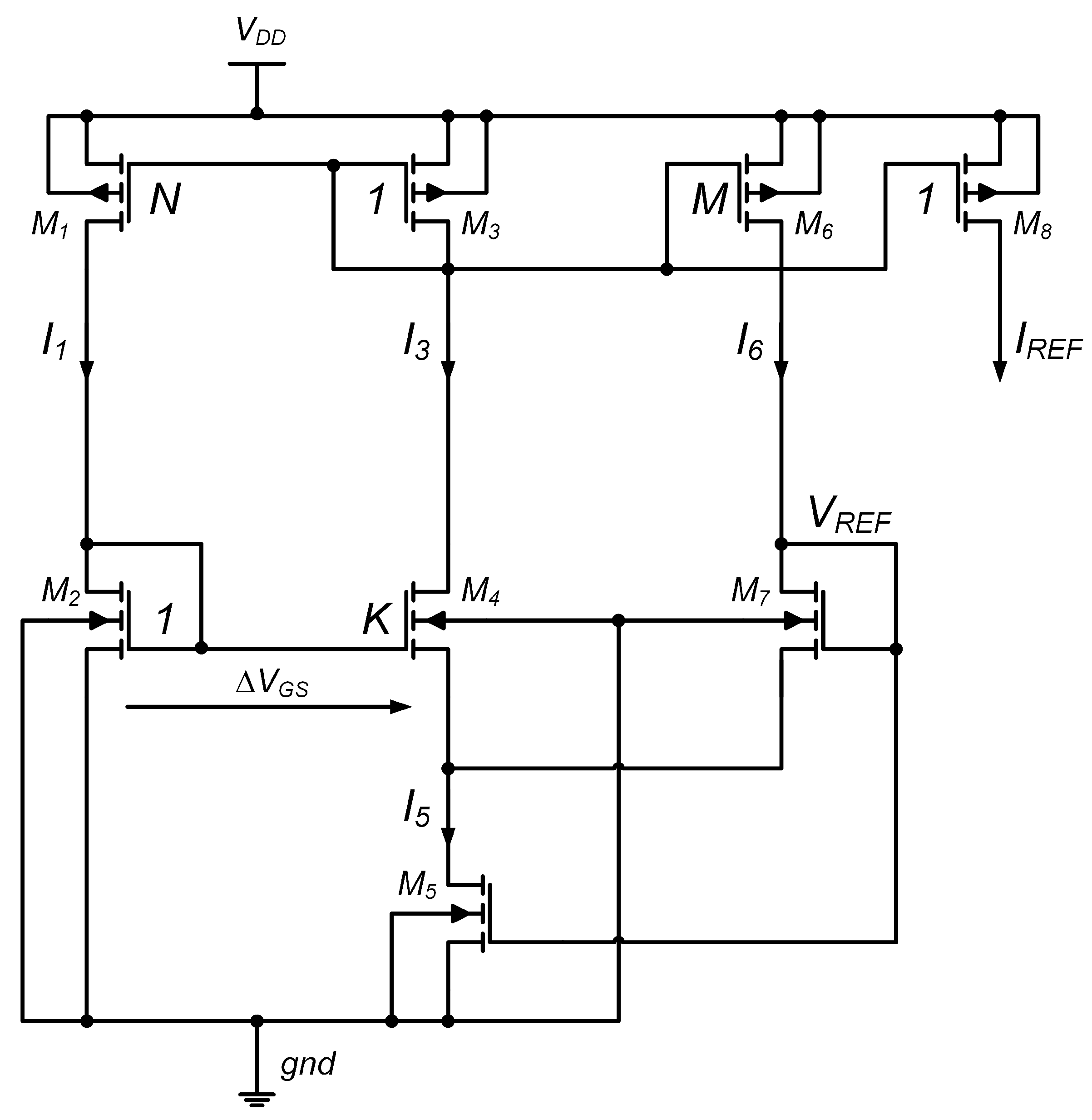
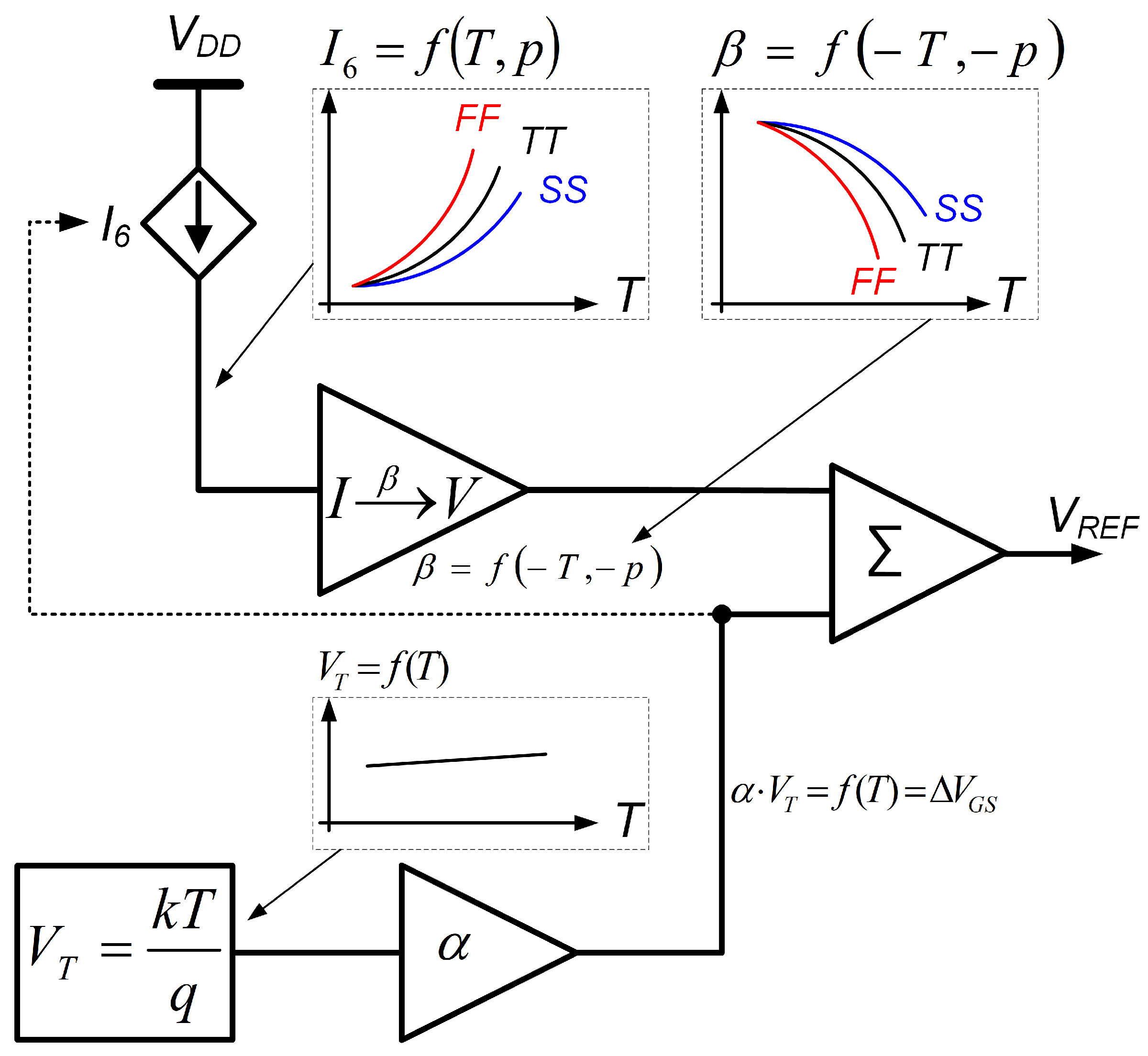
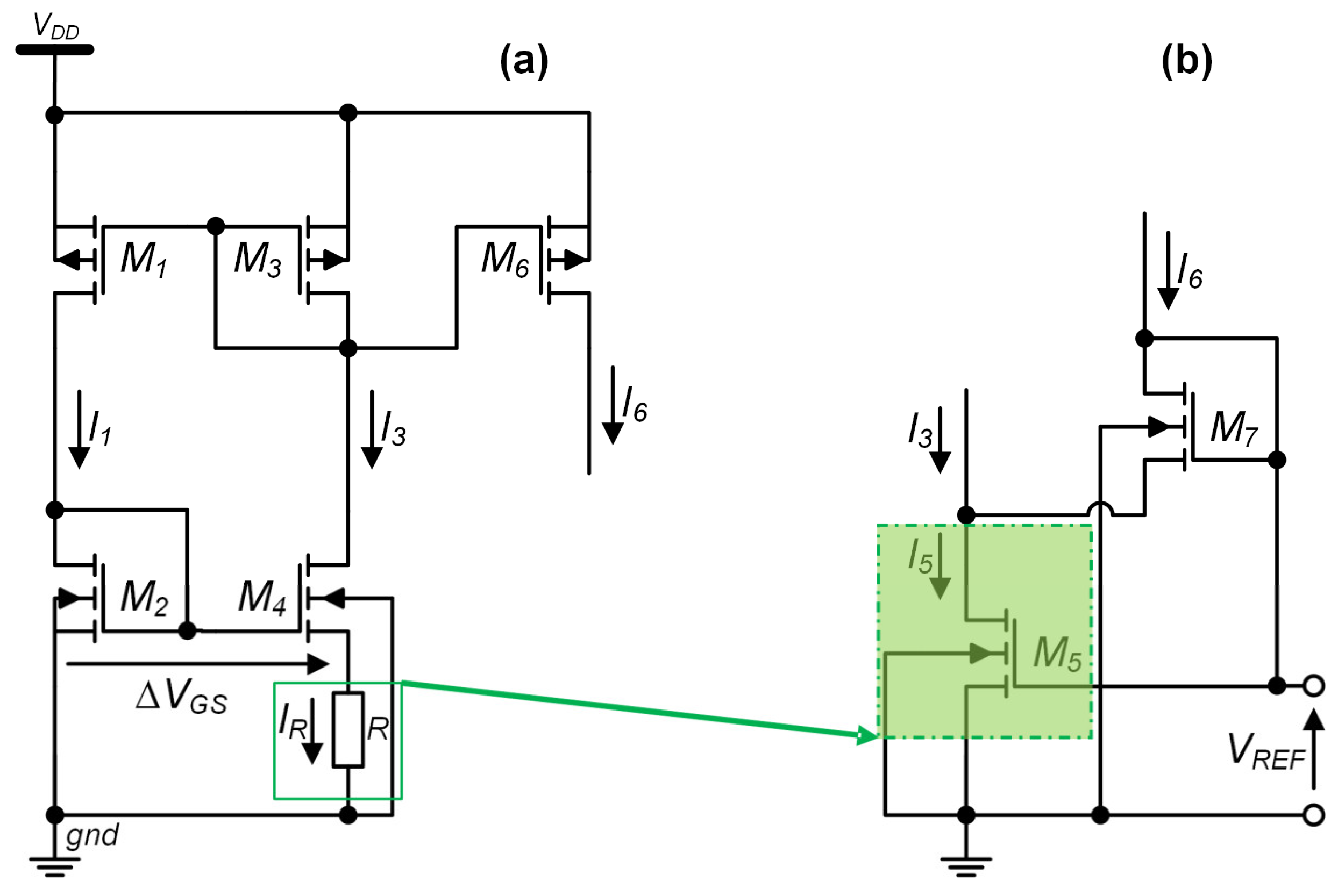
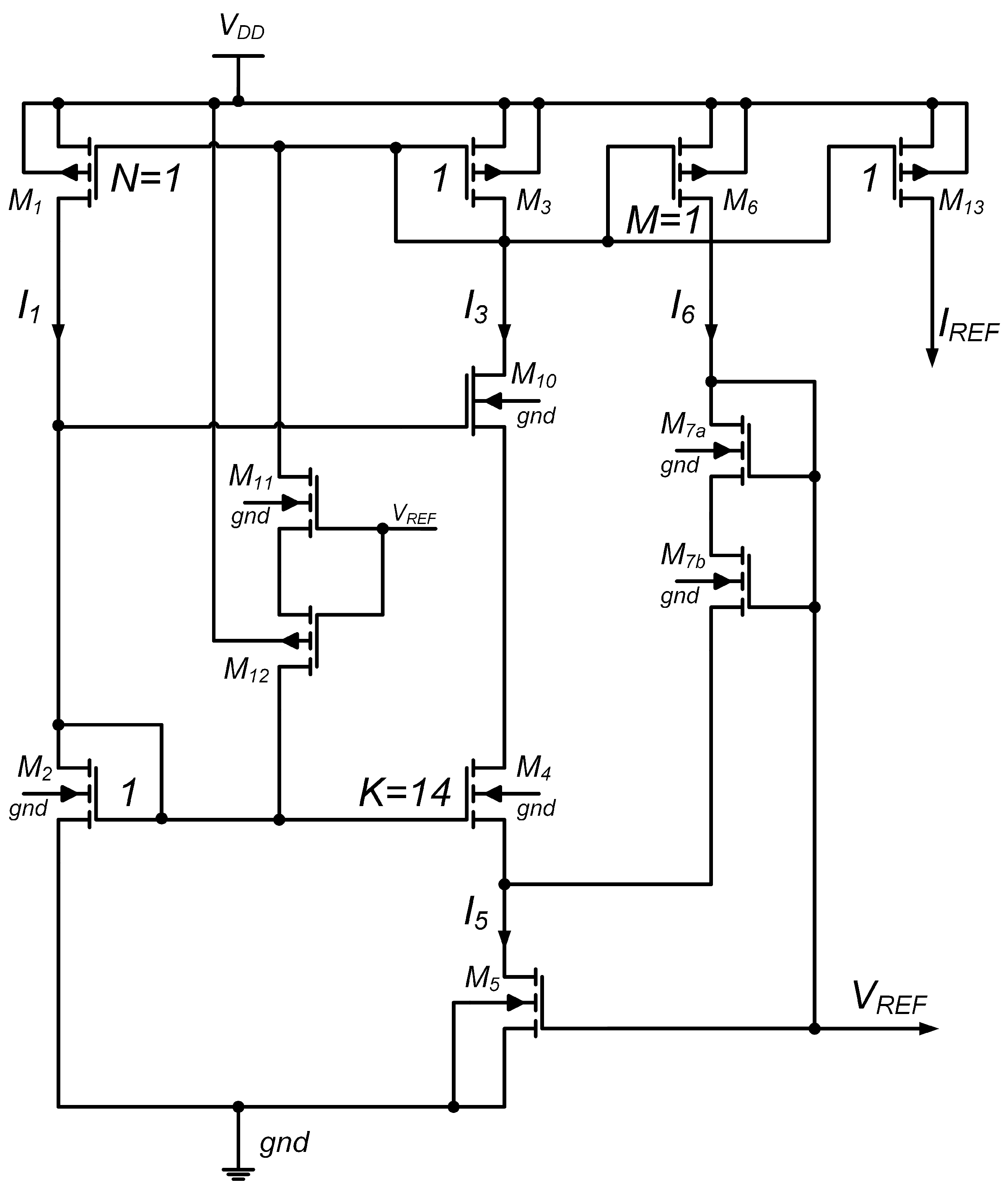
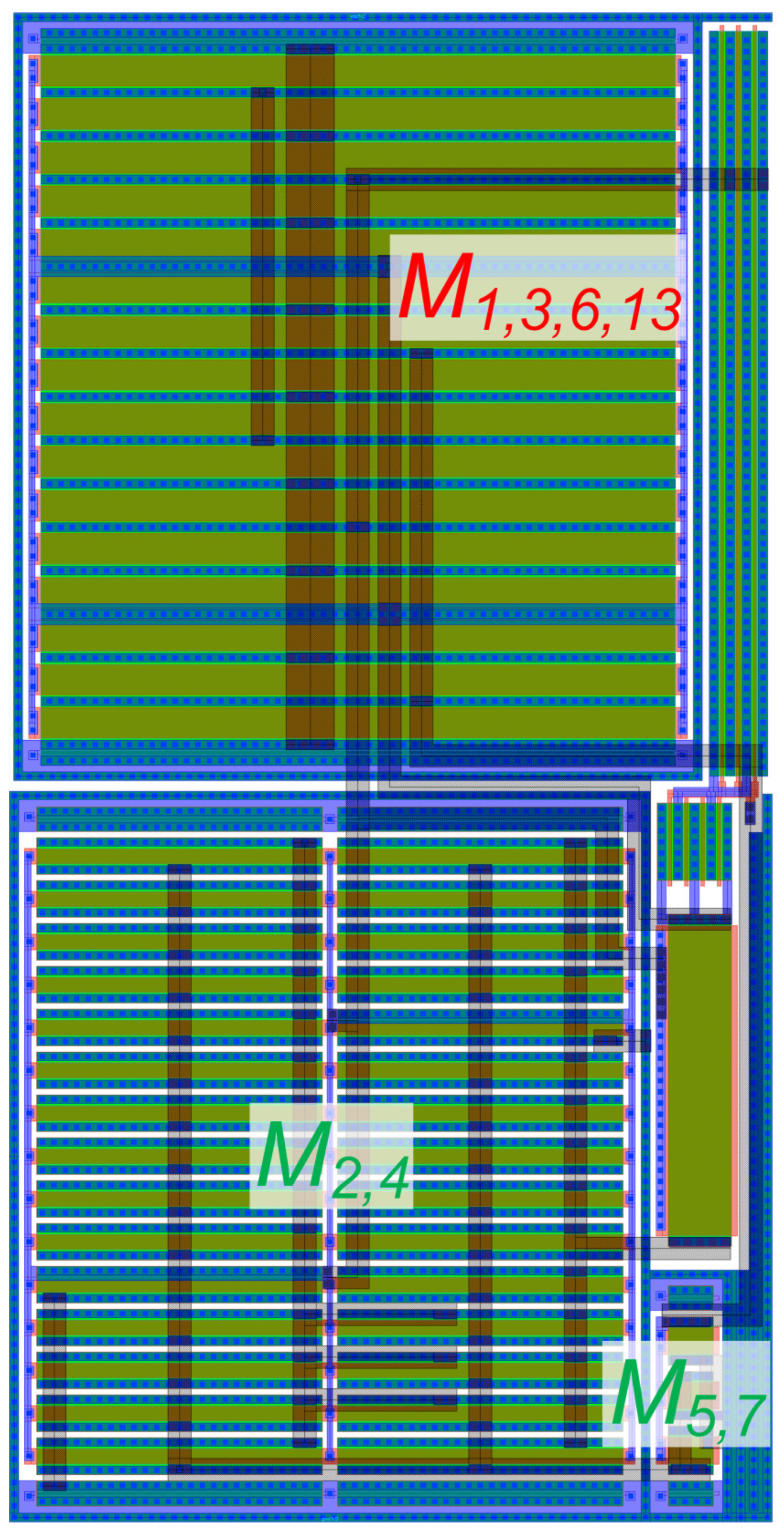
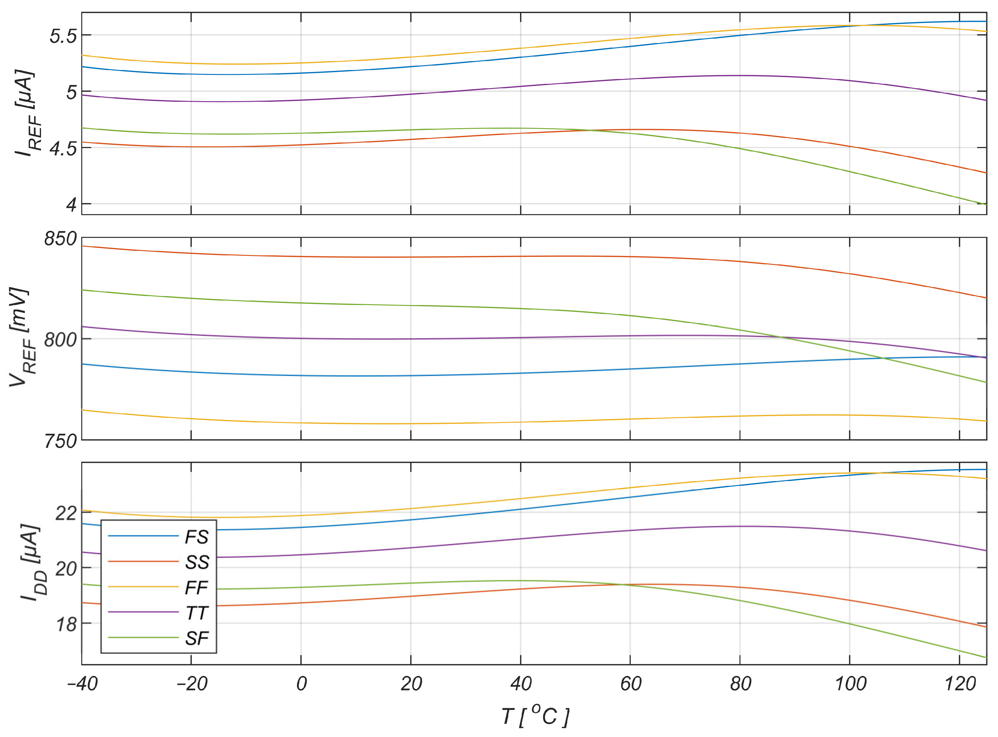
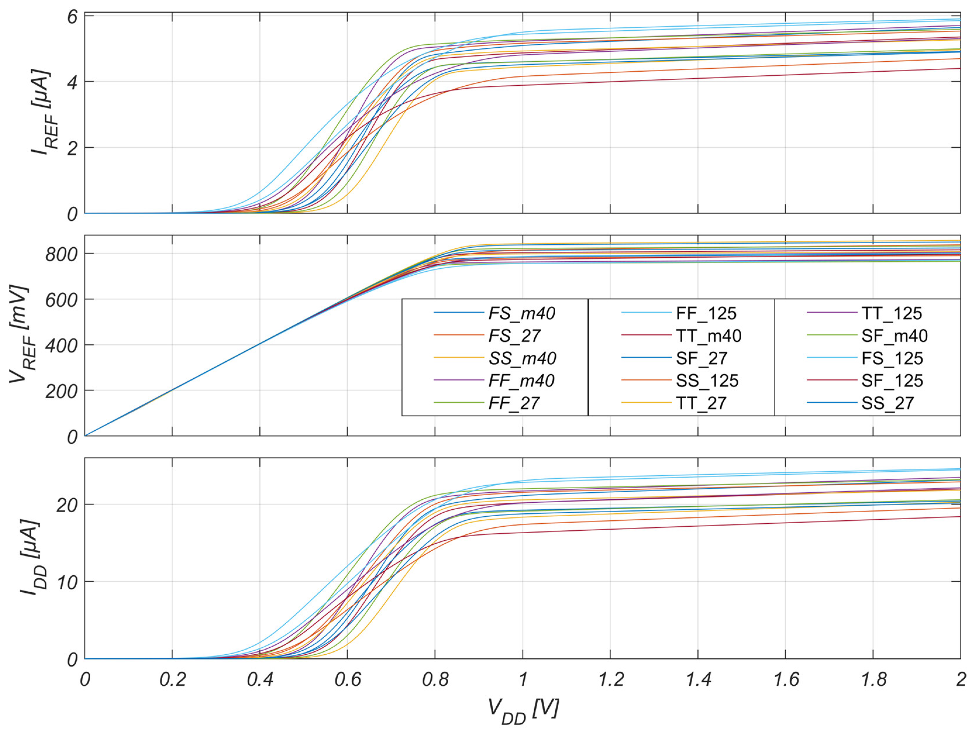
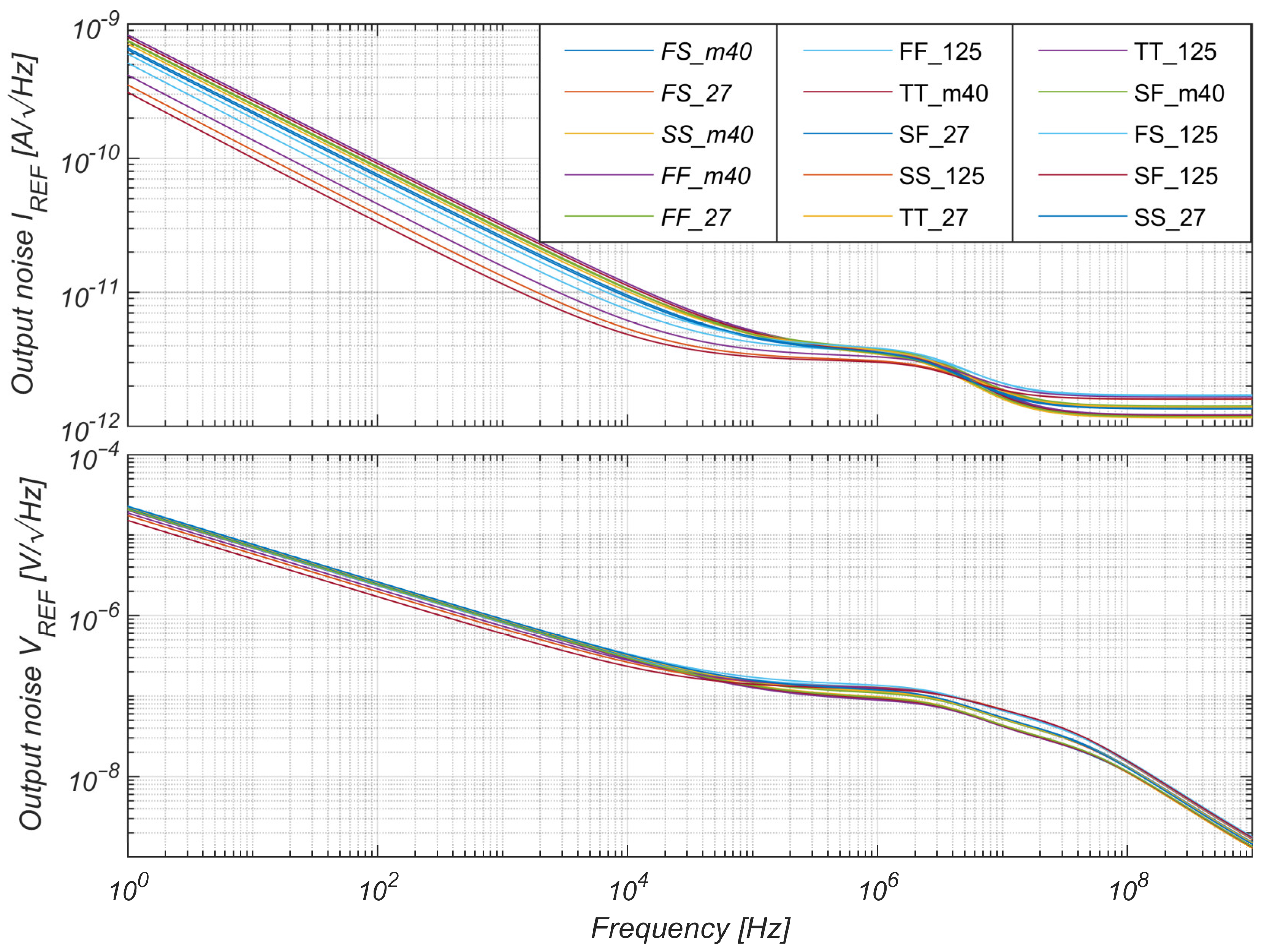
A design methodology for a resistorless low-power two-in-one voltage and current reference source working in subthreshold and moderate regions is described. The presented novel universal reference voltage–current source was implemented in ten different designs for seven different CMOS technologies. Six versions of these designs were silicon-proven using four different CMOS technologies. The example of implementation in 130 nm technology provides a reference current of 5 µA and reference voltage of 800 mV at supply voltages ranging from 0.9 V to 2.0 V with a total current consumption of 15 µA. The proposed circuit occupies a 1200 µm2 chip area and achieves 280 and 118 ppm/°C for all process corners and temperature variation from −40 °C to 125 °C. The power supply rejection ratio of output IREF without any filtering capacitor at 100 Hz and 10 MHz is 128 dB and 100 dB, respectively. The equivalent output current noise in the bandwidth from 1 Hz to 10 MHz reaches 9.1 nARMS.
Keywords: bandgap; voltage reference; current reference; integrated circuits; subthreshold bandgap; voltage reference; current reference; integrated circuits; subthreshold