Abstract
With the rapid development of modern science and technology, the stability and reliability of electronic components become essential. Low-temperature drift resistors (LTDRs) are of importance owing to their excellent performance and stability in different temperature environments. LTDR technology is now widely used in the industrial field. This paper reviews the research status of LTDRs in order to provide reference for researchers and engineers in related fields. First, the basic principle of LTDRs is briefly discussed. A brief explanation of the mechanism behind low-temperature drift is illustrated. Second, the materials, types, and manufacturing processes of LTDRs are classified and discussed. The review ends with a brief conclusion concerning the challenges from mechanism to application and the future outlook.
1. Introduction
With the rapid development of electronic information technology, analog circuits with digital-to-analog conversion and other linear or nonlinear characteristics are in great demand [1]. Especially for high-precision analog circuits, certain feedback circuits, precision measurement equipment and fine instruments, resistors with low temperature coefficients are imperative to maintain circuit precision and stability [2,3]. To improve the precision and resolution of circuits, it is essential to enhance the performance of thin-film resistors. Thus, the temperature coefficient of resistance (TCR) is very crucial for circuit functionality, as the fluctuation of ambient temperature can induce undesirable alterations in circuit performance.
High-precision thin-film resistors exhibit excellent characteristics such as high resistivity, low TCR, high stability, absence of parasitic effects, and low noise, leading to their widespread use in hybrid analog integrated circuits [4]. Low temperature drift resistors (LTDRs) are components whose resistance values exhibit minimal variation in different temperature environments. LTDRs can be applied in numerous fields, including aerospace, automotive, analog-to-digital converters, etc. For applications requiring precise measurements and calibration, high-performance LTDRs enhance circuit accuracy by mitigating errors caused by temperature fluctuations [5]. For high-precision analog circuits, variations in resistance values directly impact the output accuracy [2]. For these applications, the role of TCR is to mitigate resistance value fluctuations, ensuring circuit stability, precision, and enhanced reliability.
In this review, we aim to provide a summary of research activities concerned with LTDRs. Initially, theory and hypothesis are discussed to explain why LTDRs exhibit low temperature coefficient characteristics. Then, methods for measuring the temperature coefficient of resistance are introduced. Furthermore, various factors affecting TCR in existing technologies are analyzed, including materials and manufacturing processes. Finally, the review is concluded with some perspectives on developments in the future.
2. Theory and Hypothesis of TCR
Numerous studies have identified factors that affect the temperature coefficient in the manufacturing process. However, there are limited studies on the specific mechanisms governing how these factors influence TCR. Some theoretical hypotheses regarding factors that influence the resistive mechanism were proposed. For example, Gladun et al. found that the crystallization degree of silicon-chromium (CrSi) thin films is significantly correlated with their electrical properties [6]. With the film evolving from amorphous to polycrystalline composite, the electrical resistivity would change [7]. Moreover, in the annealing process, the formation of CrSi2 grains dictates the transport behavior. However, Cuong et al. assumed that the variation in the TCR of TiOxNy thin-film resistors is primarily attributed to changes in grain size rather than changes in the degree of crystallinity [8]. To clarify the mechanism of TCR, it can be introduced in two aspects.
2.1. Electron Mean Free Path
According to the Drude model [9], the resistivity (ρ) of a metal is given by the following formula:
where A is a constant related to the electronic structure of the metal. n is the number of free electrons per unit volume. e is the charge of an electron. λ is the mean free path of an electron, which is the average distance an electron can travel freely before being scattered by the lattice.
The electrical resistivity depends upon the “mean free path” of the electrons or the average distance that electrons can travel before they are scattered [10]. When the thickness of the material becomes sufficiently small, many properties and characteristics that it exhibits in its bulk form undergo significant changes. It comes from increased surface interactions as well as absorption and scattering effects [11]. The electrical resistivity of material in bulk form is different from that in nanoscale. It can be understood that it occurs with the mean free path of conduction electrons reduced due to increased scattering effects. Obviously, the electrical resistivity and other properties of thin films may exhibit different behaviors if the materials shrink to dimensions on the nanoscale.
The low temperature drift characteristics result from the short electron mean free path as demonstrated in some studies [12,13]. Mooji et al. found that the electrical properties of NiCr alloy in bulk and thin film have no change. It was discovered that the low TCR is an inherent characteristic of the alloy [12]. Except for NiCr, numerous disordered alloys containing transition metals exhibit similar electrical conductivities in both bulk and thin-film forms. For these materials, there is a correlation between resistivity and the temperature coefficient. It is concluded that the anomalous electrical properties of alloy resistors may be attributed to the very short mean free path of electrons in these materials. The electron mean free path is so small that it cannot be reduced any more. With temperature increasing, scattering intensifies during electron transmission. However, the electron mean free path does not decrease further, leading to a stable temperature coefficient. NiCr with a mean free path of 0.4 nm has an ultra-low value of TCR [13]. The behavior of electrical conduction in alloys with low TCR can be significantly explained by the assumption that these alloys reach a minimum electron mean free path. This minimum value must exist, as the mean free path cannot be less than the interatomic spacing based on the definition of mean free path. With the mean free path limited, any further reduction in the mean free path caused by phonons is prevented, resulting in the resistivities of different alloys differing in relatively narrow margins.
2.2. Balance between Two Temperature Coefficients
For some metal-semiconductor thin films, there is another hypothesis explaining their low temperature drift characteristics. Some studies indicate there is a balance point between regions with high and low temperature coefficients. The value of TCR can even reach zero. Nozomi et al. investigated the changes in resistivity and TCR of Cr-Si-C thin films in the annealing process [14]. It was observed that the resistivity exhibited a sudden change in the range from 450 °C to 600 °C. The peak was located at 540 °C. Around 510 °C, the TCR continuously increased, transforming from a negative to a positive value. During annealing above 450 °C, the TCR was negative in the amorphous state. As chromium silicide crystals grew, the TCR turned positive.
Thus, it is concluded that the TCR is determined by both the amorphous and crystalline phases. The TCR of the amorphous phase is negative. As shown in Figure 1, with temperature increasing, Cr-rich crystals with positive TCR appear. As the Cr-rich crystals grow larger, the resistivity decreases and TCR increases. It is determined by the balance between the amorphous regions and the crystalline regions.

Figure 1.
Schematics of microstructure and electrical current path model for Cr–Si–C films (a) as-deposited, (b) annealed at 540 °C for 10 min, and (c) annealed at 1000 °C for 10 min [14].
Figure 1.
Schematics of microstructure and electrical current path model for Cr–Si–C films (a) as-deposited, (b) annealed at 540 °C for 10 min, and (c) annealed at 1000 °C for 10 min [14].

Thus, it is concluded that the TCR is determined by the interplay between the amorphous and crystalline phases. At lower temperatures, the entire phase is in an amorphous state, where conductivity increases with temperature because the increased temperature allows charge carriers to escape their self-induced traps and hop to the next available site. As the temperature continues to increase, the phase begins to transition into a crystalline state, exhibiting more metallic characteristics. During this transition, Cr-rich crystals with a positive TCR emerge, as shown in Figure 1b. As these Cr-rich crystals grow larger, the resistivity decreases and TCR increases because the increased temperature gives rise to increased phonon-induced scattering. The entire TCR of the resistor is determined by the balance between the amorphous regions, which have a negative TCR, and the crystalline regions with a positive TCR.
In addition to thermally activated conduction, tunneling effects should also be considered. The relative contributions of these processes to the overall conductivity vary according to the degree of recrystallization and bridging between islands [15]. The deposited film comprises metallic islands embedded in a semiconductor amorphous part. Electron transport within the film occurs via activated charge-carrier generation and tunneling between the metallic islands. The tunneling effect increases with temperature, enhancing electron probability to surmount barriers and thus reducing resistance. So, it results in a negative temperature coefficient. As the metallic composition increases, the islands coalesce to form a metallic channel structure. Eventually, a continuous metallic conduction path that yields a positive temperature coefficient appears. Consequently, the balance of different parts in the resistor results in a very low TCR. In summary, the phase undergoes a transition from a negative temperature coefficient to a positive one. What we are interested in is the intermediate zone within this transition, specifically the state at zero temperature coefficient, where the balance between the amorphous and crystalline phases results in a neutral TCR.
Based on the above discussion, for thin-film resistors, there are more factors that affect their resistivity, such as grain boundary scattering [16], surface scattering [17], and impurity scattering. Adding aluminum impurities to CrSi resistors can cause significant changes in the TCR [18]. Further research is needed to develop an accurate model. Additionally, the surface morphology of thin films is critical for the performance of high-precision thin-film resistors with ultra-thin resistive layers [19]. In ultra-thin films, size effects are pronounced, with resistivity being significantly influenced by the surface roughness of the thin film.
3. Current Advances in LTDRs
3.1. Methods for Measurement and Characterization
First, it is necessary to define the physical quantity of the change in resistance with temperature.
The relationship between resistance R(T) and temperature T satisfies the following function [20]:
where is the reference resistance at 300 K, and and are the first-order and second-order coefficients, respectively. R(T) can be obtained by testing at different temperatures, and then and can be obtained by polynomial fitting. Nevertheless, another definition is widely applied, as below.
The TCR quantifies the relative variation in resistance for a 1 °C temperature increment, expressed in parts per million per degree Celsius (ppm/°C).
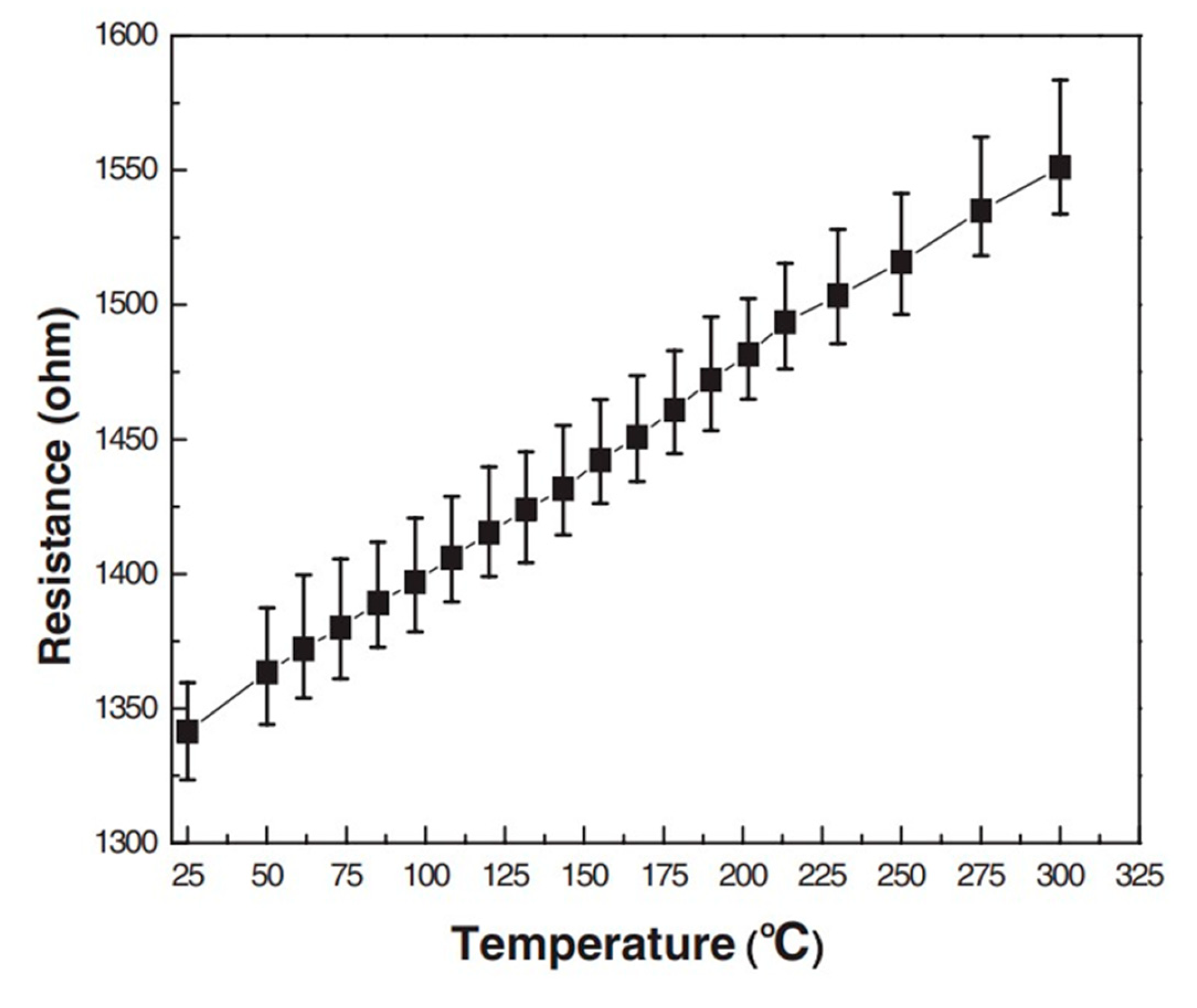
T represents the measurement temperature, while R and R0 denote the resistance at temperature T and room temperature T0, respectively. The term “ppm” signifies parts per million. Figure 2 shows the temperature dependence of the resistivity of the Ti/TiN resistor.
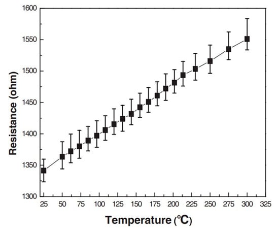
Figure 2.
The temperature dependence of the resistivity of the Ti/TiN resistor [21].
Figure 2.
The temperature dependence of the resistivity of the Ti/TiN resistor [21].
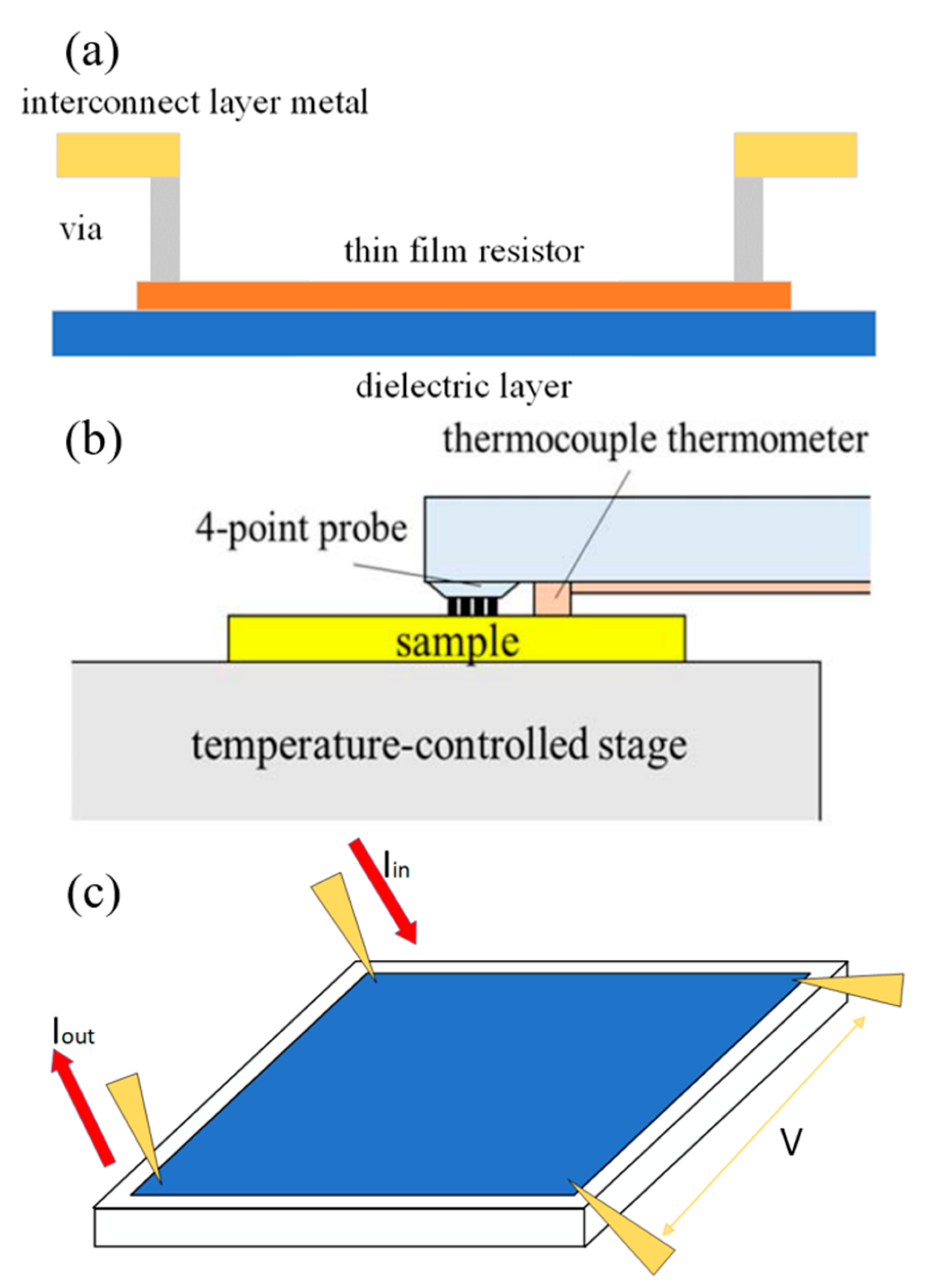
Thick-film resistors are manufactured by firing a special paste consisting of a binder, carrier, and metal oxides on a substrate [22]. Thick-film resistive glazes have environmental unfriendliness issues, with a TCR of about 100 ppm [23]. Low-temperature drift thin-film resistors include surface-mount thin-film resistors and alloy-film precision resistors, whose TCR can approach zero. In the manufacturing of integrated circuits, LTDRs are generally of the thin-film form, as shown in Figure 3a. The TCR for diffused and polysilicon resistors can reach absolute values exceeding 250 ppm [2,24], whereas thin-film resistors offer a broader range of sheet resistance (from 10 Ω/sq to 100 kΩ/sq), lower and adjustable TCR, superior tolerance, enhanced reproducibility, linear electrical behavior, and reduced parasitic capacitance values. Square resistance is defined as the resistance between opposite sides of a square-shaped conductive film. It is a measure of the resistivity of the material per unit thickness and is an important parameter for characterizing thin-film conductors. The square resistance is a characteristic that remains constant regardless of the size of the square. It solely depends on the material’s resistivity and the thickness of the film. The standard formula for calculating square resistance is
The material’s resistivity () is quantified in Ohm-meters (Ω⋅m), and the film thickness (d) is specified in meters (m).
Next, techniques such as the four-point probe method [25] and the Van der Pauw method [26] are utilized in measuring resistance, as shown in Figure 3b,c. The four-point probe method is a direct technique for measuring the resistivity of materials, particularly suitable for thin films and surface layer resistivity assessments. This method employs four probes equally spaced apart, making contact with the sample surface—two for current injection and the other two for voltage measurement. Consequently, this approach minimizes the impact of contact resistance on the measurement results. The Van der Pauw method is a more sophisticated technique capable of measuring the resistivity of samples of any shape, including thin films and irregularly shaped specimens. This approach typically utilizes a set of current probes and a set of voltage probes at the periphery of the sample. By measuring the voltage and current at different locations, the sample’s resistivity can be calculated. By measuring the resistance values at different temperatures, we can obtain the TCR. Changing the temperature typically requires a sealed, stable chamber.

Figure 3.
Schematics of (a) thin film resistor, (b) four-point probe method [14] and (c) the Van der Pauw method for TCR measurement [27].
Figure 3.
Schematics of (a) thin film resistor, (b) four-point probe method [14] and (c) the Van der Pauw method for TCR measurement [27].
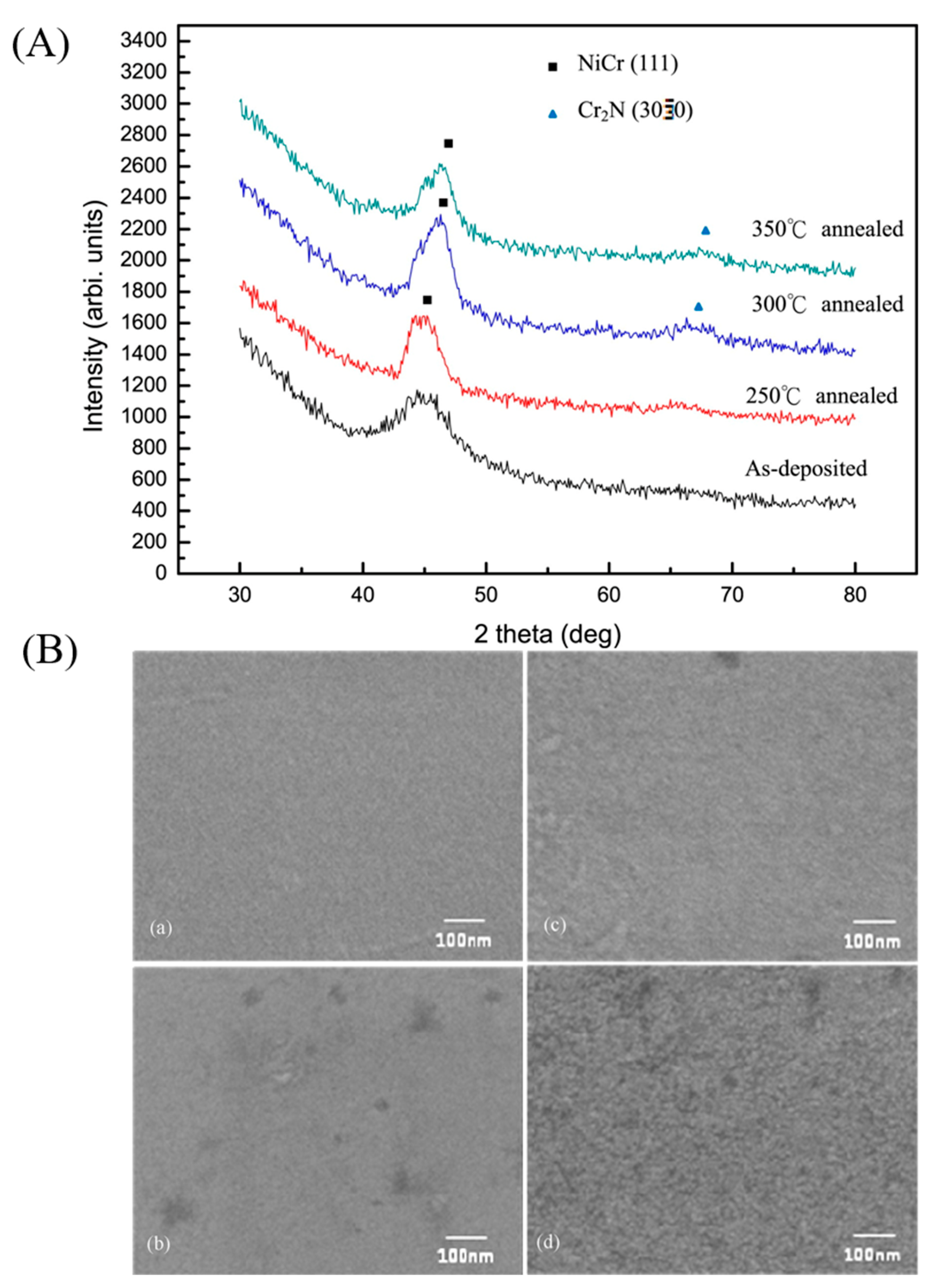
Characterization of thin-film resistors can be accomplished through various methods. For instance, X-ray diffraction (XRD) can be utilized to determine the crystal lattice structure as shown in Figure 4, unit cell dimensions, etc. [28,29]. We can employ scanning electron microscopy (SEM) to examine the surface morphology of the samples and utilize X-ray photoelectron spectroscopy (XPS) for the identification of specific elements and for valence state analysis [30].
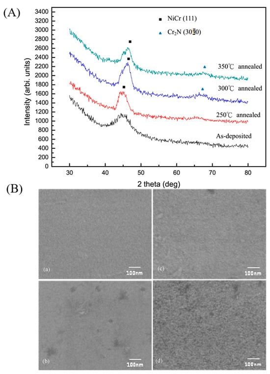
Figure 4.
(A) XRD pattern of 30 nm thickness of Ni–Cr film sputtered at 500 W and various annealing temperatures; and (B) SEM image of Ni–Cr film [31].
Figure 4.
(A) XRD pattern of 30 nm thickness of Ni–Cr film sputtered at 500 W and various annealing temperatures; and (B) SEM image of Ni–Cr film [31].
3.2. Types and Composition of Materials in LTDRs
Different types of materials, like metallic elements, alloys, and organic substances, possess varying electrical properties. The TCR of an alloy is typically less than the TCR of a metal, as shown in Table 1. Thus, LTDRs are generally made of alloy materials. Low temperature drift thin-film resistors are found including NiCr, TaN, SiCr, and other materials [32]. Each material has a different resistivity, but all have a minimal temperature coefficient, allowing them to be used for fabricating LTDRs with various resistance values.

Table 1.
Different materials with resistivity and TCR [12,32].
Table 1.
Different materials with resistivity and TCR [12,32].
| Material | Resistivity (μΩ·cm) | TCR (ppm/°C) |
|---|---|---|
| Cu | 0.000172 | >3900 |
| Ag | 0.000158 | 3800 |
| Ni | 0.00068 | 6900 |
| Cr | 0.00129 | 3000 |
| CuNi | 110 | <100 |
| AlV | 200 | <100 |
| CrNi | 110 | <100 |
| CuGe | 100 | <100 |
| CrSi | 2600 | 200 |
| MoSi | 1300 | 125 |
However, the data in this table are not absolute, because as the film resistance thickness, material composition ratio and other factors change, the electrical properties will also change accordingly, as shown in Table 2.

Table 2.
Comparison of resistance of different materials [32].
Table 2.
Comparison of resistance of different materials [32].
| Square Resistor Resistance | Film Material |
|---|---|
| 200 Ω/sq | MoSi2/NiCr |
| 2 kΩ/sq | SiCr/Cr-SiO |
| 20 kΩ/sq | SiCr |
To prevent oxidation of thin-film resistors, which could affect their electrical properties, a passivation layer is typically deposited over the resistors to isolate them from oxygen. For instance, in SiCr, the formation of an amorphous SiO2 structure reduces the pathways for grain boundaries and oxygen diffusion, thereby enhancing the oxidation resistance [33].
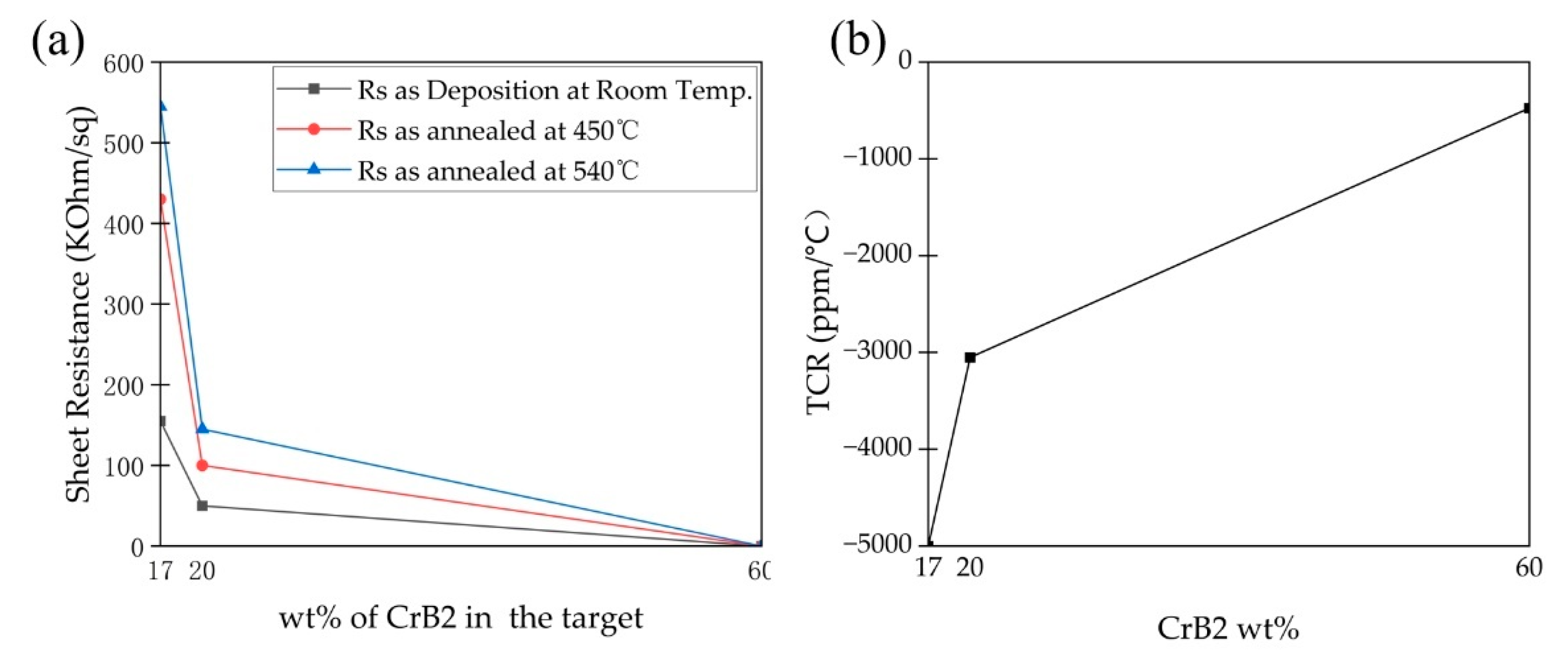
Adjusting the composition ratio of an alloy can modify the resistance value and temperature coefficient [1,3]. Choi et al. doped Mn into Bi4Ti3O12 thin films to mitigate the impact of oxygen vacancies on the film’s performance. They successfully reduced the leakage current, enhancing the electrical properties of the thin film [34]. Guangke et al. discovered that doping ZrB2 thin-film resistors with silver (Ag) can decrease the resistance of the thin film. ZrB2 has a negative TCR, while Ag has a positive TCR. Furthermore, when the atomic percentage of the doped silver is 33.9%, the thin-film resistor exhibits a temperature coefficient close to zero [35]. As shown in Table 3, Waits altered the ratio of silicon to chromium in SiCr resistors. They found that when the atomic percentage of chromium (at%) is at 27%, the TCR approaches zero. As shown in Figure 5, the effect of the target composition (CrB2 component) on the resistance and TCR is significant.
Most materials currently used for LTDRs are alloys. In recent years, some new materials have been discovered with a lower temperature coefficient, such as polycrystalline ceramics [23,36]. Searching for new materials may become a new direction in LTDR research.

Table 3.
The relationship between the chromium (Cr) percentage in SiCr resistors and their resistivity as well as temperature coefficient [37].
Table 3.
The relationship between the chromium (Cr) percentage in SiCr resistors and their resistivity as well as temperature coefficient [37].
| at. % Cr | ρ (Ω·cm) | TCR (ppm/℃) |
|---|---|---|
| 30 | 0.0058 | +100 |
| 27 | 0.0074 | ~0 |
| 25 | 0.0095 | −100 |
| 19 | 0.026 | −500 |
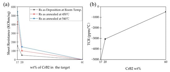
Figure 5.
(a) Sheet resistance vs. CrB2 percentage in the target at different annealing temperatures. (b) TCR vs. CrB2 percentage in the target [38].
Figure 5.
(a) Sheet resistance vs. CrB2 percentage in the target at different annealing temperatures. (b) TCR vs. CrB2 percentage in the target [38].
3.3. Fabrication of LTDRs
Many studies in the literature emphasize reducing TCR through the fabrication process. The impact of process parameters on the performance of resistors is extremely significant. Fabrication methods for thin-film resistors encompass a variety of techniques. They include chemical approaches such as thermal oxidation [39],chemical vapor deposition [40], electroplating, and anodic reaction deposition, as well as physical methods like vacuum evaporation [41], sputtering [42], ion beam [43], epitaxy [44], etc. Different fabrication methods for thin films can yield films with varying properties. Even for the same material, due to differences in homogeneity, defects, and internal stress caused by deposition, LTDR performance can vary greatly. The choice of fabrication method must be tailored to the desired properties of the thin film. Taking low temperature drift resistors of SiCr as an example, the industrial standard typically involves magnetron sputtering, followed by high-temperature annealing for fabrication. In the fabrication of CuNi resistive thin films, Hur et al. found that varying deposition temperatures resulted in distinct temperature coefficients of resistance [25]. Y. C. Kwon et al. discovered that the sputtering power also affects the TCR of the resistor, as shown in Figure 6a [5]. They sputtered SiCr resistors under conditions of 100 W, 200 W, and 300 W, using the same annealing conditions, and ultimately found that the TCR decreased with increasing sputtering power.

Figure 6.
(a) SiCr resistor sputtering power and TCR relationship [5]. (b) Resistivity of the deposited 28 Cr-72 Si 40 Cr-60 Si and 55 Cr-45 thin-film resistors. (c) Temperature coefficients of resistivity (TCR) of the deposited CrSi-based thin-film resistors [3].
Figure 6.
(a) SiCr resistor sputtering power and TCR relationship [5]. (b) Resistivity of the deposited 28 Cr-72 Si 40 Cr-60 Si and 55 Cr-45 thin-film resistors. (c) Temperature coefficients of resistivity (TCR) of the deposited CrSi-based thin-film resistors [3].

Interestingly, Wang et al. experimentally observed that as the sputtering power for SiCr increased, the temperature coefficient of resistance of the resistors increased [45]. This may be related to other conditions during the resistor’s fabrication process. In summary, the factors mentioned above are interrelated and collectively influence the electrical properties of the thin film.
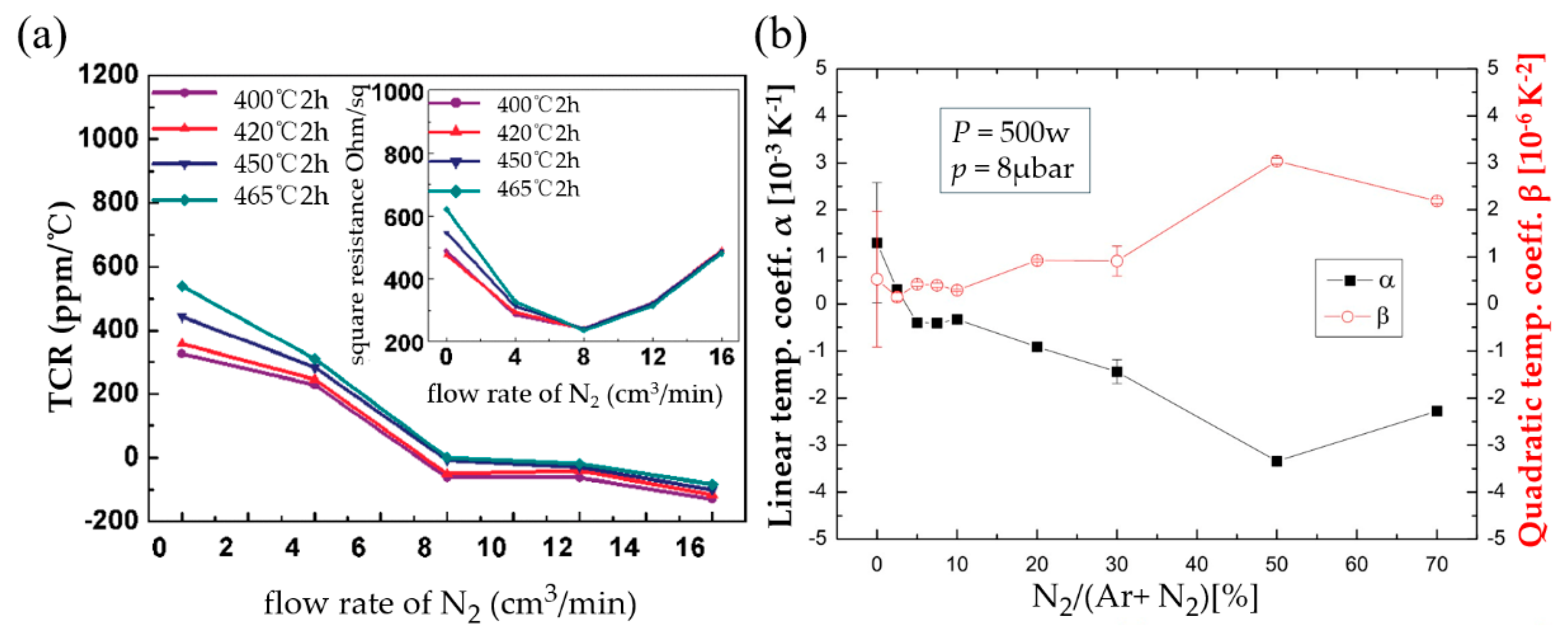
Cuong et al. discovered that altering the nitrogen/argon flow ratios during Ti sputtering can induce a phase variation from Ti to TiN in thin-film resistors. Therefore, modifying the TCR is possible, as shown in Figure 7a [46]. J. Zhu et al. modified the sputtering atmosphere in their experiments with SiCr resistors. They observed that the introduction of nitrogen led to the formation of SiNx components in the final thin film. The nitrogen doping partially suppressed the growth of CrSi grains, which had a significant impact on the TCR of the thin-film resistor [4].
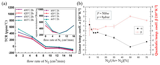
Figure 7.
(a) TCR and square resistance of CrSi films under various experimental conditions [4]. (b) Results for TCR dependent on partial nitrogen content [47].
Figure 7.
(a) TCR and square resistance of CrSi films under various experimental conditions [4]. (b) Results for TCR dependent on partial nitrogen content [47].
To achieve a low temperature coefficient and stable resistive film quality, thermal treatment of thin-film resistors is imperative. Generally, the growth process of thin films introduces various crystal defects, which can be mitigated through annealing to reduce the defects present during film growth. Proper thermal treatment is essential for amorphous films produced by sputtering to stabilize their properties. As shown in Figure 8, different annealing temperatures lead to different resistance and TCR. Vanden presented evidence that structural change happened in CrSiO films during annealing [48]. With the formation of the dielectric phase in the CrSiO thin films, their electrical properties changed.
Films deposited at lower temperatures tend to form small islands. Because the lower mobility of the islands prevents them from moving, they remain in place where they first land on the substrate. As annealing progresses, small, continuous film structures coalesce into an island structure, leading to a significant change in resistance, as shown in Figure 9 [38]. Sonoda et al. observed that [49] with annealing, the crystalline phase of SiCr resistive thin films gradually transitions from the initial amorphous Cr1−xSix to the polycrystalline phase Cr5Si, and with further increases in annealing temperature, ultimately to CrSi2, as shown in Figure 10a. The amorphous Cr1−xSix exhibits a higher resistivity and a positive temperature coefficient, whereas Cr5Si3 and CrSi2 have lower resistivity and a negative temperature coefficient of resistance. Broek’s discovery of irreversible changes in the electrical properties of films as annealing proceeds confirms this claim [50]. Different annealing atmospheres can also affect the performance of resistors, as shown in Figure 11. Lai found the best annealing conditions for NiCr resistors include annealing in N2 atmosphere, at a temperature of 250 °C. With the annealing time of 540 s, the TCR varied between −220.8 and 444.2 ppm/K [51].

Figure 8.
Variation in (a) resistivity as a function of annealing temperature. (Inset) Product of carrier concentration and mobility as a function of annealing temperature. (b) TCR and hysteresis of resistance in the TiNxOy thin films as a function of annealing temperature [8]. (c) TCR variation at the sputtering power of 200 W for 30 min annealing time according to the annealing temperature [5].


Figure 9.
Resistance measurement during heat treatment. (a) Resistance changes during heat treatment of a 20 nm Si70Cr30 film in air. Time changes as indicated by the numbers, l–2 being the first heating step and so on. The rise that starts at 275 °C is caused by crystallization of the CrSi2 phase. This phase is also responsible for the increasing curvature in the higher branches in (a); the curvature is defined as dTCR/dT [50]. (b) Resistivity annealing curves for (i) the electron-beam co-evaporated CrSi3 alloy film, and (ii) the Cr/Si bilayer on thermally oxidized silicon wafer substrate. The broken lines are reversible cooling curves. In the figure, (A)–(D) indicate the different stages of the annealing process [28].
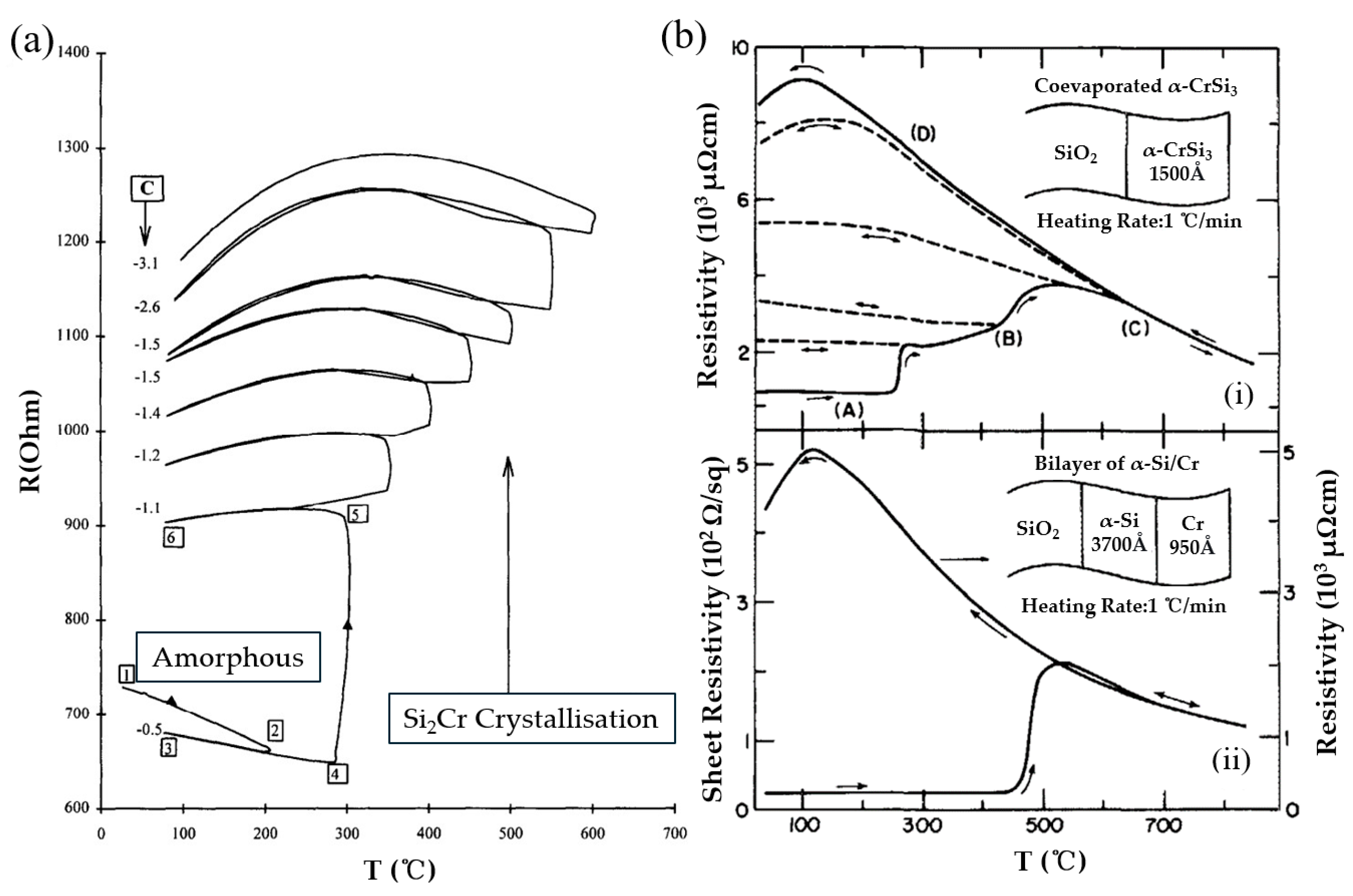

Figure 10.
(a) Schematic diagram of the phase transitions during annealing. (b) The resistivity of the thin film as a function of the annealing temperature. The resistivity is normalized by the measured value of the as-deposited sample. (c) The TCR of the thin film as a function of the annealing temperature. The TCR is normalized by the absolute measured value of the as-deposited sample [49].


Figure 11.
The temperature dependence of the TCR of Ni–Cr embedded thin-film resistor: (a) 540 s × N2; (b) 300 °C × N2; (c) 540 s × air [51].
Figure 11.
The temperature dependence of the TCR of Ni–Cr embedded thin-film resistor: (a) 540 s × N2; (b) 300 °C × N2; (c) 540 s × air [51].

As shown in Table 4, different manufacturing processes, the magnitude of current used, and ambient temperature can all lead to varying resistivity results in resistors. Further research is needed to understand the mechanisms behind these variations.

Table 4.
Comparison of DC electromigration for SiCr resistors [2].
Table 4.
Comparison of DC electromigration for SiCr resistors [2].
| Resistor Type | Thickness (nm) | Resistivity (Ohm·cm) | Current (A/cm2) | Tambient (°C) | Tresistor (°C) | EA (eV) |
|---|---|---|---|---|---|---|
| Cr(70%)Si(30%) | 5 | 5.5 × 10⁻³ | 1.0 × 10⁷ | 25 | \ | \ |
| CrSi | 10 | 2.0 × 10⁻³ | 3.2 × 10⁶ | 150–225 | 380–480 | 3.0 |
| CrSi | 10 | 2.7× 10⁻⁴ | 1.0 × 10⁷ | \ | 386 | 1.46 |
| CrSi | <10 | <1.5 × 10⁻³ | 1.0 × 10⁷ | 190–230 | n/a | 0.71–0.84 |
4. Conclusions and Outlook
The LTDR has made significant advancements, yet it continues to present a complex interplay of material properties, fabrication techniques, and the control of microstructural attributes. The intrinsic characteristics of materials such as NiCr, TaN, and SiCr have been better understood through meticulous research, leading to the development of resistors with minimal TCR.
Despite the progress, several challenges remain in the development and application of LTDRs. The accurate mechanisms behind low-temperature drift are not yet fully elucidated. It is necessary to pursue further research to obtain a more accurate physical model. A deeper comprehension of how the microstructure affects resistivity and temperature coefficients could enable improvements in fabrication processes, potentially reducing grain boundary scattering and enhancing film uniformity. Thus, achieving higher precision and consistency in resistive performance is possible [52]. Future research directions can include the exploration of innovative material systems, the refinement of fabrication methodologies, and a more profound investigation into the underlying physical mechanisms that govern temperature-dependent resistive variations. This could enable the development of LTDRs with a lower TCR, at a lower cost and with greater precision. Additionally, it is necessary to strengthen studies on the long-term stability and reliability of LTDRs to ensure their sustained performance in practical applications [2,53]. Custom-designed LTDR solutions for specialized applications, such as aerospace, medical equipment, and precision measurement, will be vital. Many systems in extreme environments require LTDRs to maintain their stability. The future of LTDR technology is poised for growth, with the potential to significantly enhance the performance and reliability of electronic systems in different temperature environments.
Author Contributions
Conceptualization, F.L.; Investigation, B.W. and Y.D.; Methodology, F.L.; Project administration, K.X.; Supervision, K.X.; Writing—original draft, L.Z.; Writing—review and editing, L.Z. and K.X. F.L. and L.Z. contribute equally to this work. All authors have read and agreed to the published version of the manuscript.
Funding
This research was supported by Laboratory Specialized Scientific Research Projects of Beijing Smart-chip Microelectronics Technology Co., Ltd., (No. SGSC0000YFQT2402513).
Data Availability Statement
The data presented in this study are available on request from the corresponding author.
Conflicts of Interest
Author Fang Liu, Bo Wu and Yongfeng Deng was employed by Beijing Smartchip Microelectronics Technology Co., Ltd. The remaining authors declare that the research was conducted in the absence of any commercial or financial relationships that could be construed as a potential conflict of interest and the authors declare that this study received funding from Beijing Smartchip Microelectronics Technology Co., Ltd. The funder was not involved in the study design, collection, analysis, interpretation of data, the writing of this article or the decision to submit it for publication.
Correction Statement
This article has been republished with a minor correction to the Funding statement. This change does not affect the scientific content of the article.
References
- Cheng, H.Y.; Chen, Y.C.; Li, C.L.; Li, P.J.; Houng, M.P.; Yang, C.F. Developments of the Physical and Electrical Properties of NiCr and NiCrSi Single-Layer and Bi-Layer Nano-Scale Thin-Film Resistors. Nanomaterials 2016, 6, 39. [Google Scholar] [CrossRef] [PubMed]
- Stewart, K.A.; Kimura, K.; Ring, M.; Noldus, K.; Hulse, P.; Jerome, R.C.; Hasegawa, A.; Gambino, J.P.; Price, D.T. Assessing SiCr resistor drift for automotive analog ICs. In Proceedings of the 2021 IEEE International Reliability Physics Symposium (IRPS), Monterey, CA, USA, 21–25 March 2021. [Google Scholar] [CrossRef]
- Tseng, H.W.; Feng, D.J.Y.; Li, C.L.; Yang, C.F. Effects of deposition parameters on properties of high resistance CrSi-based thin-film resistors. Int. J. Mod. Phys. B 2021, 35, 2150040. [Google Scholar] [CrossRef]
- Zhu, J.; Zhang, Z.; He, N.; Zhang, S.; Gu, L.; Zhang, L. Electrical Properties of CrSi Thin Film Resistors for High Precision Analog Circuits. In Proceedings of the 2022 10th International Symposium on Next-Generation Electronics (ISNE), Wuxi, China, 12–14 May 2023; pp. 1–3. [Google Scholar]
- Kwon, Y.C.; Seol, H.C.; Hong, S.K.; Kwon, O.K. Process Optimization of Integrated SiCr Thin-Film Resistor for High-Performance Analog Circuits. IEEE T Electron. Dev. 2014, 61, 8–14. [Google Scholar] [CrossRef]
- Gladun, C.; Heinrich, A.; Schumann, J.; Pitschke, W.; Vinzelberg, H. Transport-Properties of Nanodisperse Crxsi1-X Thin-Films. Int. J. Electron. 1994, 77, 301–308. [Google Scholar] [CrossRef]
- Burkov, A.T.; Vinzelberg, H.; Schumann, J.; Nakama, T.; Yagasaki, K. Strongly nonlinear electronic transport in Cr-Si composite films. J. Appl. Phys. 2004, 95, 7903–7907. [Google Scholar] [CrossRef]
- Cuong, N.D.; Kim, D.J.; Kang, B.D.; Yoon, S.G. Structural and electrical properties of TiNxOy thin-film resistors for 30 dB applications of π-type attenuator. J. Electrochem. Soc. 2006, 153, G856–G859. [Google Scholar] [CrossRef]
- Belser, R.B.; Hicklin, W.H. Temperature Coefficients of Resistance of Metallic Films in the Temperature Range 25° to 600°C. J. Appl. Phys. 1959, 30, 313–322. [Google Scholar] [CrossRef]
- Lacy, F. Evaluating the Resistivity-Temperature Relationship for RTDs and Other Conductors. IEEE Sens. J. 2011, 11, 1208–1213. [Google Scholar] [CrossRef]
- Lacy, F. Developing a theoretical relationship between electrical resistivity, temperature, and film thickness for conductors. Nanoscale Res. Lett. 2011, 6, 636. [Google Scholar] [CrossRef]
- Mooij, J.H. Electrical-Conduction in Concentrated Disordered Transition-Metal Alloys. Phys. Status Solidi A 1973, 17, 521–530. [Google Scholar] [CrossRef]
- Nocerino, G.; Singer, K.E. The electrical and compositional structure of thin Ni-Cr films. Thin Solid. Films 1979, 57, 343–348. [Google Scholar] [CrossRef]
- Ito, N.; Maekawa, K.; Kunimune, Y.; Hasegawa, E.; Abe, K.; Shiraishi, N.; Takahashi, Y.; Tonegawa, T.; Tsuchiya, Y.; Inoue, M. The effect of microstructures on the electrical properties of Cr-Si-C thin film resistors. Jpn. J. Appl. Phys. 2022, 61, SJ1004. [Google Scholar] [CrossRef]
- Glang, R.; Holmwood, R.A.; Herd, S.R. Resistivity and Structure of Cr-Sio Cermet Films. J. Vac. Sci. Technol. 1967, 4, 163–170. [Google Scholar] [CrossRef]
- Devries, J.W.C. Resistivity of Thin Au Films as a Function of Grain Diameter and Temperature. J. Phys. F Met. Phys. 1987, 17, 1945–1952. [Google Scholar] [CrossRef]
- Fuchs, K. The conductivity of thin metallic films according to the electron theory of metals. P. Camb. Philos. Soc. 1938, 34, 100–108. [Google Scholar] [CrossRef]
- Ma, H.; Ma, Y.; Han, X.; Chen, J.; Yang, Z.; Ta, S.W.; Zhang, Y.; Zhang, Z.Y.; Cao, Z. Influence of Al doping and annealing on the microstructures and electrical properties of CrSi films prepared by magnetron co-sputtering. Vacuum 2023, 210, 111904. [Google Scholar] [CrossRef]
- Chung, K.C.; Lee, W.H. Effect of pretreatment on Al2O3 substrate by depositing Al2O3 film on the properties of Ni-Cr-Si based thin film resistor. Mater. Chem. Phys. 2019, 234, 311–317. [Google Scholar] [CrossRef]
- Gao, C.W.; Zhang, D.C. Establishment and verification of resistance temperature coefficient model of P-type non-uniformly doped resistance. J. Micromech. Microeng. 2022, 32, 105006. [Google Scholar] [CrossRef]
- Cheng, Y.L.; Wei, B.J.; Shih, F.H.; Wang, Y.L. Stability and Reliability of Ti/TiN as a Thin Film Resistor. Ecs J. Solid. State Sc. 2013, 2, Q12–Q15. [Google Scholar] [CrossRef]
- Sumida, T. Recent Advances in Thick-Film Resistors and Target Applications. IEEE Power Electron. 2022, 9, 70–72. [Google Scholar] [CrossRef]
- Lu, Y.; Li, Y.; Peng, R.; Shi, L.; Li, F.; Chen, D.; Wen, Q.; Yang, C.; Yang, Q. Low temperature coefficient of resistance and high conductivity: Enhanced Cu–substituted LaCo0.4Ni0.6O3 ceramics for functional material. Ceram. Int. 2022, 48, 27899–27904. [Google Scholar] [CrossRef]
- Uang, C.-W.; Chuang, H.-M.; Shen-Fu, T.; Thei, K.-B.; Lai, P.-H.; Fu, S.-I.; Tsai, Y.-Y.; Liu, W.-C. Temperature-dependent characteristics of diffused and polysilicon resistors for ULSI applications. In Proceedings of the Fourth International Workshop on Junction Technology, 2004. IWJT’04, Shanghai, China, 16 March 2004; pp. 293–296. [Google Scholar]
- Hur, S.G.; Kim, D.J.; Kang, Y.D.; Yoon, S.G. Effect of the deposition temperature on temperature coefficient of resistance in CuNi thin film resistors. J. Vac. Sci. Technol. B 2004, 22, 2698–2701. [Google Scholar] [CrossRef]
- Ramadan, A.A.; Gould, R.D.; Ashour, A. On the Van der Pauw method of resistivity measurements. Thin Solid. Films 1994, 239, 272–275. [Google Scholar] [CrossRef]
- Sun, Y.-C.; Zhang, L.-Z. Measurement of sheet resistance for microa- reas by using a modified van der pauw’s method. Acta Phys. Sin. 1994, 43, 530–539. [Google Scholar] [CrossRef]
- Nava, F.; Tien, T.; Tu, K.N. Temperature-Dependence of Semiconducting and Structural-Properties of Cr-Si Thin-Films. J. Appl. Phys. 1985, 57, 2018–2025. [Google Scholar] [CrossRef]
- Jankowski, A.F.; Hayes, J.P. Ti-Cr-Al-O thin film resistors. Thin Solid. Films 2002, 420, 487–491. [Google Scholar] [CrossRef]
- Perillo, P.M.; Rodriguez, D.F. Influence of low temperature annealing time on CdS thin films. Physica B 2024, 680, 415828. [Google Scholar] [CrossRef]
- Chuang, N.C.; Lin, J.T.; Chen, H.R. TCR control of Ni-Cr resistive film deposited by DC magnetron sputtering. Vacuum 2015, 119, 200–203. [Google Scholar] [CrossRef]
- Waits, R.K. Silicide Resistors for Integrated Circuits. Pract. Inst. Electr. Elect. 1971, 59, 1425–1429. [Google Scholar] [CrossRef]
- Chang, L.C.; Sung, M.C.; Chen, Y.I. Effects of bias voltage and substrate temperature on the mechanical properties and oxidation behavior of CrSiN films. Vacuum 2021, 194, 110580. [Google Scholar] [CrossRef]
- Choi, J.Y.; Choi, C.H.; Cho, K.H.; Seong, T.G.; Nahm, S.; Kang, C.Y.; Yoon, S.J.; Kim, J.H. Effect of oxygen vacancy and Mn-doping on electrical properties of Bi4Ti3O12 thin film grown by pulsed laser deposition. Acta Mater. 2009, 57, 2454–2460. [Google Scholar] [CrossRef]
- Tian, G.K.; Shi, T.T.; Li, X.Y.; Lu, X.B.; Wang, Y.Y.; Liu, C. Low resistivity and near-zero temperature drift ZrB2-Ag composite films prepared by DC magnetron co-sputtering. Mater. Lett. 2022, 307, 130992. [Google Scholar] [CrossRef]
- Liang, Z.W.; Yang, S.A.; Wang, H.S.; Li, Y.L.; Li, J.F.; Hou, B.K.; Li, J.H.; Wang, J.; Wu, L.; Zhang, H.; et al. Temperature coefficient of resistance improvement in La0.67Ca0.33MnO3 polycrystalline ceramics with vanadium addition. Ceram. Int. 2023, 49, 13578–13585. [Google Scholar] [CrossRef]
- Waits, R.K. Sputtered Silicon-Chromium Resistive Films. J. Vac. Sci. Technol. 1969, 6, 308–315. [Google Scholar] [CrossRef]
- Wu, F.; McLaurin, A.W.; Henson, K.E.; Managhan, D.G.; Thomasson, S.L. The effects of the process parameters on the electrical and microstructure characteristics of the CrSi thin resistor films: Part I. Thin Solid. Films 1998, 332, 418–422. [Google Scholar] [CrossRef]
- Mott, N. Mechanisms for the Oxidation of Silicon and the Formation of Charged Defects. Proc. R. Soc. Lon. Ser.-A 1981, 376, 207–215. [Google Scholar] [CrossRef]
- Fang, Y.K.; Hsu, S.L. Observations on the Phase-Transformation and Its Effect on the Resistivity of Wsi2 Films Prepared by Low-Pressure Chemical Vapor-Deposition. J. Appl. Phys. 1985, 57, 2980–2982. [Google Scholar] [CrossRef]
- Ghandhi, S.K.; Field, R.J.; Shealy, J.R. Highly Oriented Zinc-Oxide Films Grown by the Oxidation of Diethylzinc. Appl. Phys. Lett. 1980, 37, 449–451. [Google Scholar] [CrossRef]
- Mol, H.A.; Sarro, P.M.; Schellevis, H.; Hou, Y. Process for low temperature deposition of Strain Gauge materials based on Chromium Nitride Thin Films. In Proceedings of the ENSORS, 2011 IEEE, Limerick, Ireland, 28–31 October 2011; pp. 226–229. [Google Scholar]
- Anttila, A.; Koskinen, J.; Lappalainen, R.; Hirvonen, J.P.; Stone, D.; Paszkiet, C. Comparison of diamond-like coatings deposited with c+ and various hydrocarbon ion-beams. Appl. Phys. Lett. 1987, 50, 132–134. [Google Scholar] [CrossRef][Green Version]
- Fitzgerald, E.A.; Xie, Y.H.; Green, M.L.; Brasen, D.; Kortan, A.R.; Michel, J.; Mii, Y.J.; Weir, B.E. Totally Relaxed Gexsi1-X Layers with Low Threading Dislocation Densities Grown on Si Substrates. Appl. Phys. Lett. 1991, 59, 811–813. [Google Scholar] [CrossRef]
- Wang, F.; Chen, J.; Wang, X.; Chang, X.; Ran, M.; Yang, Y.; Yang, W. Preparation technology of CrSi thin film resistor with low temperature coefficient. Micronanoelectron. Technol. 2017, 54, 355–359. [Google Scholar] [CrossRef]
- Cuong, N.D.; Kim, D.J.; Kang, B.D.; Yoon, S.G. Effects of nitrogen concentration on structural and electrical properties of titanium nitride for thin-film resistor applications. Electrochem. Solid. St. 2006, 9, G279–G281. [Google Scholar] [CrossRef]
- Stöber, L.; Konrath, J.P.; Krivec, S.; Patocka, F.; Schwarz, S.; Bittner, A.; Schneider, M.; Schmid, U. Impact of sputter deposition parameters on molybdenum nitride thin film properties. J. Micromech. Microeng. 2015, 25, 074001. [Google Scholar] [CrossRef]
- Vanden, N.; Heinrich, A.; Klostermann, K.; Sobe, G. Ir Absorption in Crsio Thin-Films. Phys. Status Solidi A 1986, 93, 163–170. [Google Scholar] [CrossRef]
- Sonoda, K.; Shiraishi, N.; Maekawa, K.; Ito, N.; Hasegawa, E.; Ogata, T. Modeling electrical resistivity of CrSi thin films. Solid. State Electron. 2022, 198, 108471. [Google Scholar] [CrossRef]
- van den Broek, J.J.; Donkers, J.J.T.M.; van der Rijt, R.A.F.; Janssen, J.T.M. Metal film precision resistors: Resistive metal films and a new resistor concept. Philips J. Res. 1998, 51, 429–447. [Google Scholar] [CrossRef]
- Lai, L.F.; Zeng, W.J.; Fu, X.Z.; Sun, R.; Du, R.X. Annealing effect on the electrical properties and microstructure of embedded Ni-Cr thin film resistor. J. Alloy Compd. 2012, 538, 125–130. [Google Scholar] [CrossRef]
- Brynsvold, R.R.; Manning, K. Constant-current stressing of SiCr-based thin-film resistors: Initial “Wearout” investigation. IEEE Trans. Device Mater. Reliab. 2007, 7, 259–269. [Google Scholar] [CrossRef]
- Li, Y.; Huiskamp, P. A novel degradation mechanism in SiCr-O based thin film resistors under temperature and current stress. In Proceedings of the 2012 IEEE International Reliability Physics Symposium (IRPS), Anaheim, CA, USA, 15–19 April 2012. [Google Scholar]
Disclaimer/Publisher’s Note: The statements, opinions and data contained in all publications are solely those of the individual author(s) and contributor(s) and not of MDPI and/or the editor(s). MDPI and/or the editor(s) disclaim responsibility for any injury to people or property resulting from any ideas, methods, instructions or products referred to in the content. |
© 2024 by the authors. Licensee MDPI, Basel, Switzerland. This article is an open access article distributed under the terms and conditions of the Creative Commons Attribution (CC BY) license (https://creativecommons.org/licenses/by/4.0/).
