1. Introduction
Medium-voltage direct current (MVDC) distribution networks are quickly evolving into complex systems where various DC power sources and loads are interconnected. This evolution is crucial for enhancing the efficiency and reliability of modern power systems. MVDC distribution networks are particularly important in applications such as those in marine, military, and industrial settings due to their high power density and low power loss advantages [
1]. Consequently, there is a critical need to improve the stability and reliability of MVDC distribution networks. As the power sources and loads interconnected with the MVDC grid increase, the frequent fluctuations and the risk of faults also increase, which impacts the stability of the MVDC distribution network significantly [
2]. Currently, several ongoing studies are focusing on fault diagnosis and protection algorithms for various converters associated with the MVDC network [
3,
4,
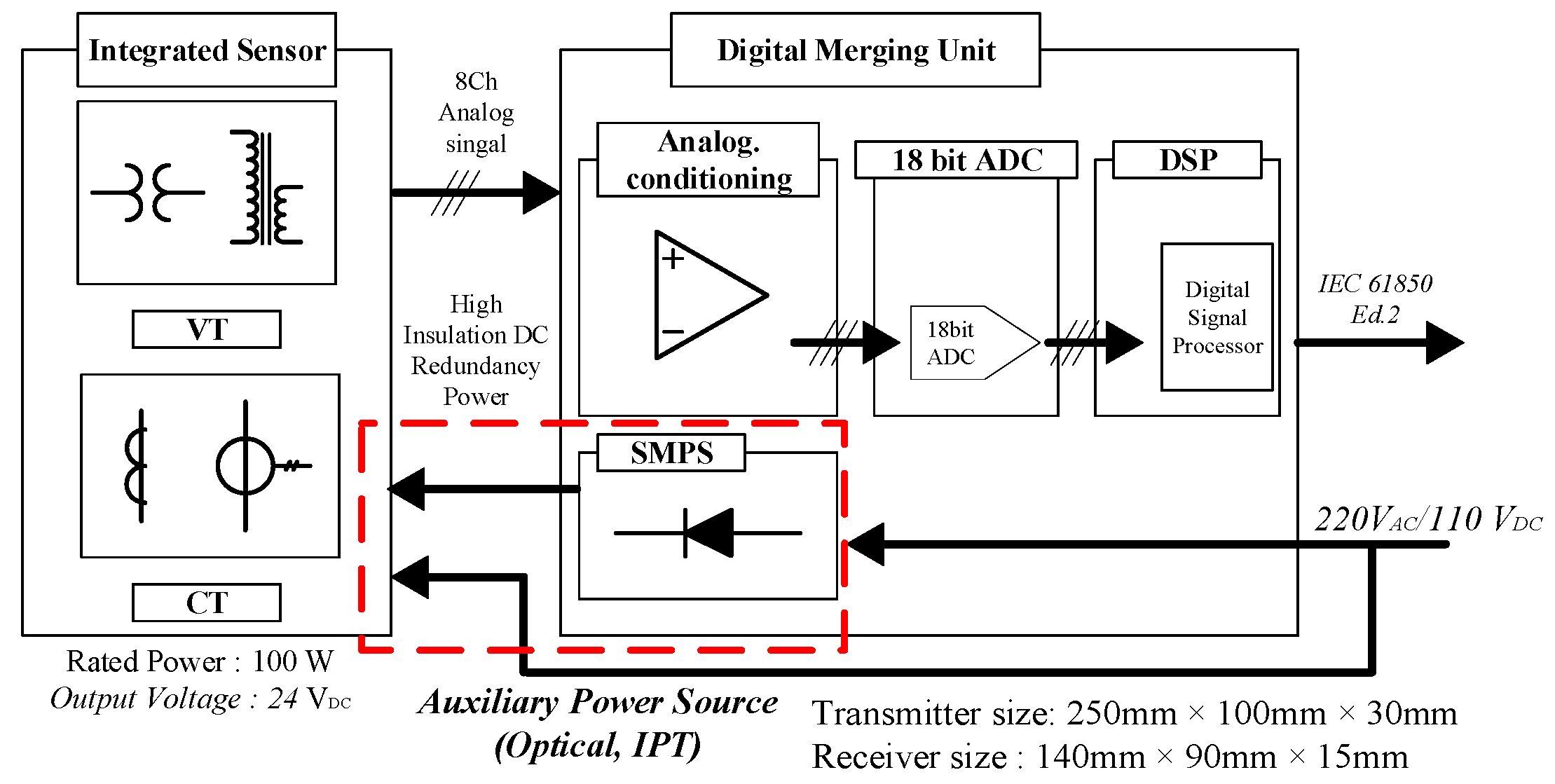
5]. The existence of these studies confirms the critical importance of high-performance sensors, as reliable fault diagnosis and protection algorithms depend heavily on the accurate and timely detection provided by such sensors. The digital merging unit system described in
Figure 1 incorporates an integrated network of sensors and auxiliary electronic circuits. To ensure high reliability, Hall-effect current sensors are employed, securing high-voltage insulation between the MVDC distribution network and the digital merging unit system.
In general, in peripheral interconnected circuits such as MVDC and voltage sensors, along with optical components such as optical converters, optical fibers and resonant beams are used as auxiliary power sources to meet high-voltage insulation requirements [
6,
7,
8]. Ref. [
6] proposed using optical converters for powering IoT sensors, while [
7] and [
8] suggested a method of transmitting both power and data together via optical converters. However, currently, commercialized optical converters typically offer only low-rated output and efficiency.
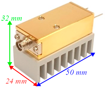
Table 1 shows the specifications of commonly used optical converters. They deliver an output of approximately 5 W with low efficiency (26%). Additionally, in the case of optical fiber cables, exposure to external environmental conditions can lead to performance degradation as the cables age.
Table 2 shows the electrical specifications of the MVDC sensor. The sensor currently consumes 44 W of power; however, due to potential performance improvements and an increase in the number of sensors, the total power consumption could rise to 100 W. As the power demand increases and the rated voltage rises from 5 V to 24 V, significant limitations often arise in terms of supplying power through optical conversion methods. Therefore, a 100 W auxiliary power system, which meets the high-performance sensor specifications and satisfies high-voltage insulation standards, would be highly desirable.
In this paper, an inductive power transfer (IPT) system with a compact design is proposed to solve these challenges. The IPT system ensures effective voltage insulation between power sources and load sensors. Constructing the IPT to supply constant power during sensor operation involves integrating it into a digital merging unit while maintaining a compact design with a fixed vertical separation distance of 100 mm. Various pad designs are proposed and compared to achieve high power density. Based on realistically achievable mutual inductance (M) ranges from the designed (coil) pad, a compensation topology that meets the requirements is determined. Furthermore, by applying an integrated coil structure with optimal efficiency and high-power density considering the rated input and output characteristics, the IPT system is experimentally verified to have an efficiency of 69.5% and a rated power of 100 W. Finally, the proposed IPT system is compared with conventional optical converters to validate the feasibility of implementing it.
The structure of this paper is as follows:
Section 2 contains the design and implementation of the proposed IPT system.
Section 4 presents the experimental results and analysis, and
Section 5 discusses the conclusions of this study and directions for future research.
2. Basic Analysis of Wireless Power Transfer
2.1. Basic Analysis of the IPT System
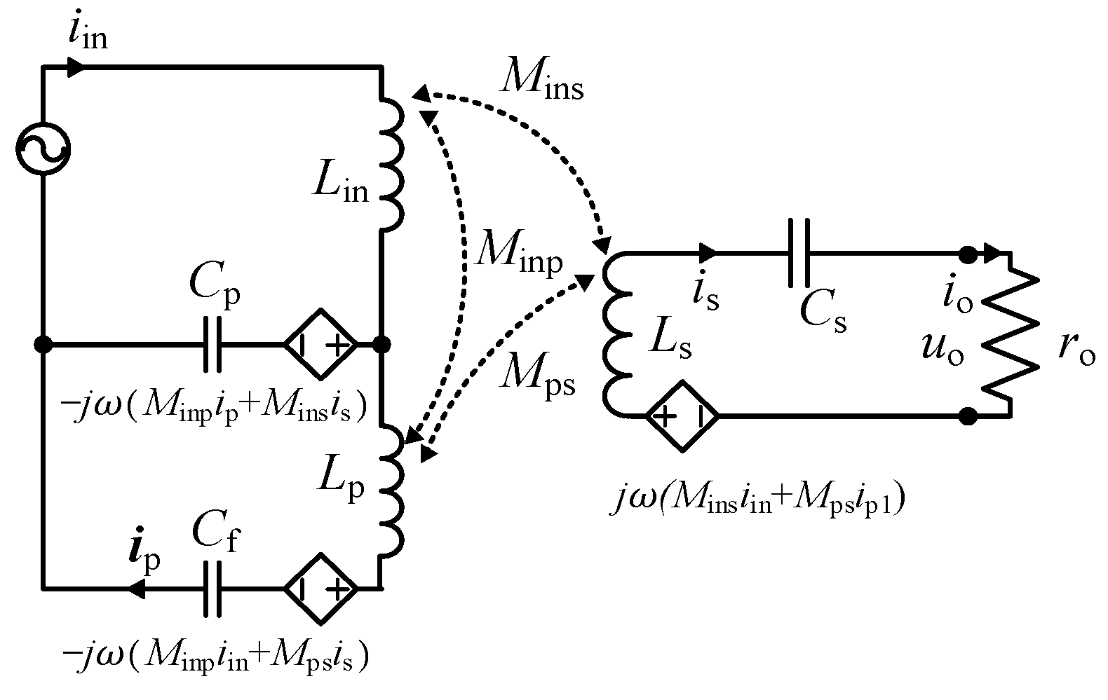
Figure 2 shows a schematic of an IPT converter. The entire system consists of an inverter that converts DC to AC power, a primary/secondary wireless pad that transmits power via electromagnetic induction, a primary/secondary resonant network that compensates for pad reactance for high-frequency operation, and a rectifier that converts AC power to DC. A typical IPT converter generates an AC voltage at the operating frequency required by the IPT system through either a half-bridge consisting of two MOSFETs or a full-bridge inverter consisting of four MOSFETs. The input AC voltage is a square wave with a fixed duty cycle of 0.5. This square wave includes various harmonics in the fundamental switching frequency waveform. However, since the passive components that make up the IPT converter act as filters, only the fundamental frequency component is transferred to the secondary side, and harmonics are assumed to be zero. Therefore, the output voltage waveform of the inverter can be approximated by Equation (1), including only the fundamental component. For a half-bridge inverter,
n = 1 is used, whereas
n = 2 is used for a full-bridge inverter.
The output AC waveform from the inverter induces a magnetic field through the time-varying current in the primary pad. The red dot in
Figure 2 indicates the polarity. This magnetic flux is coupled to the secondary pad, inducing an electromotive force (EMF) and causing current to flow. The mutual inductance (
M) between the primary pad current (
ip) and secondary pad current (
is) in loosely coupled transformer (LCT) is determined by their mutual magnetic interaction, where
k is the coupling coefficient representing the efficiency of magnetic coupling between the primary and secondary pads.
M is a crucial factor that determines the output characteristics and is given by the following equation:
The EMF induced on the secondary side passes through a resonant network, which reduces harmonics and is then rectified and smoothed into direct current (DC) by the rectifier. The output characteristics vary depending on the structure of the rectifier. Hence, the output DC characteristics can be calculated as shown in Equation (3), where a half-bridge rectifier is represented by
m = 1, and a full-bridge rectifier is represented by
m = 2.
UL is DC load voltage, and
IL is DC load current.
2.2. Wireless Pad Design
The value of k between the primary and secondary pad affects M. Therefore, it is important to minimize the variation in k due to fluctuations in separation distance when designing a wireless pad.
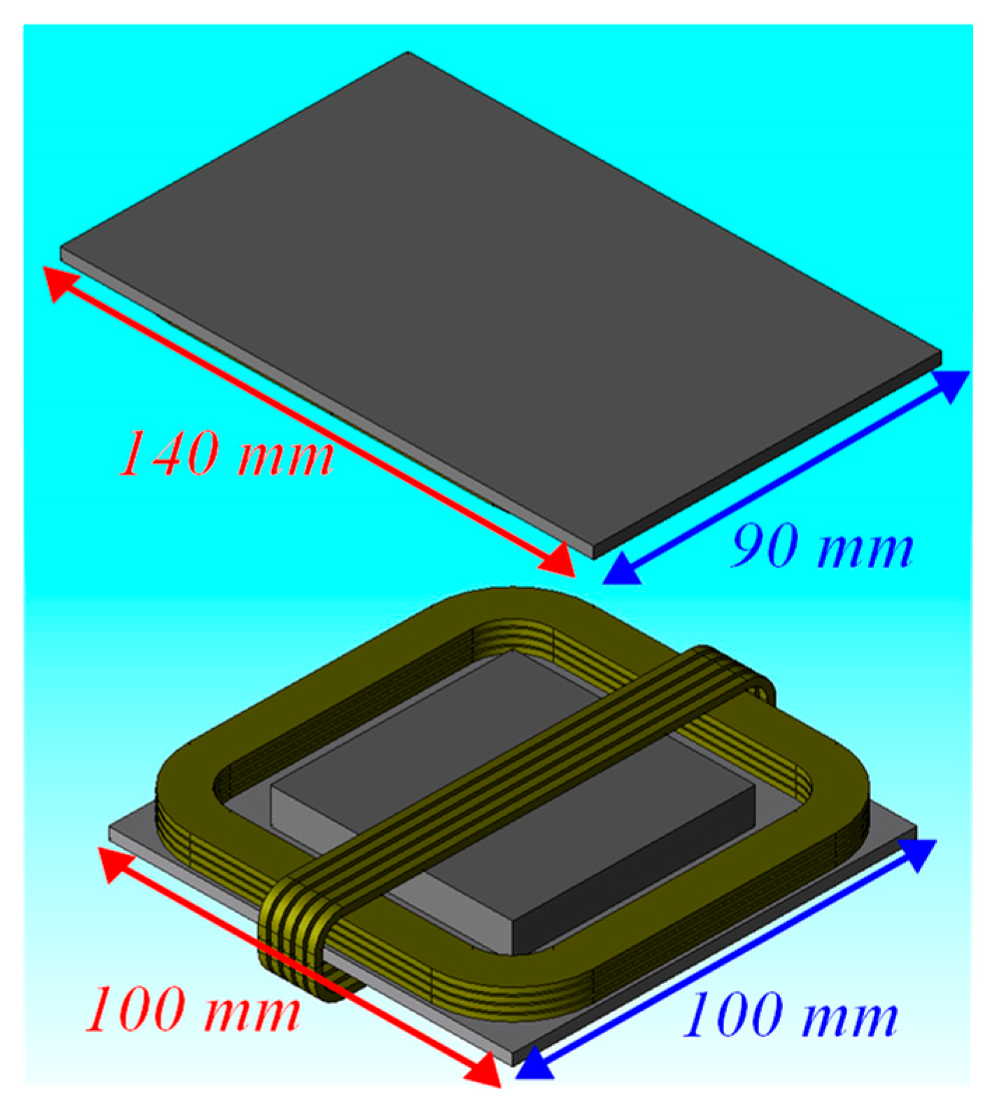
Figure 3 shows a 3D configuration of the integrated sensor. Given that the MVDC voltage applied to the power distribution line can reach 100 kV, it is crucial to ensure an adequate (and constant) air insulation distance. According to [
9], a minimum separation distance of 3 kV/mm must be maintained for sufficient air insulation. In this paper, considering a feasible placement location and separation distance for the primary pad, a vertical separation distance of 100 mm is selected.
The wireless pad can utilize several different IPT 3-D pad designs, as shown in
Table 3. The pads are classified into unipolar and multipolar pads based on the structure that radiates magnetic flux.
Table 4 shows the FEM simulated
k values for each pad design. Note that when the polarities are different, the magnetic flux of the pads cancels out, and no power is transmitted. Therefore, simulations for pads with different polarities are not conducted. The simulation results show that the RP-RP design, which has the largest outer diameter within the limited pad area, features the highest
k (0.0280). Therefore, the basic design for the wireless pad in this paper is set to RP-RP.
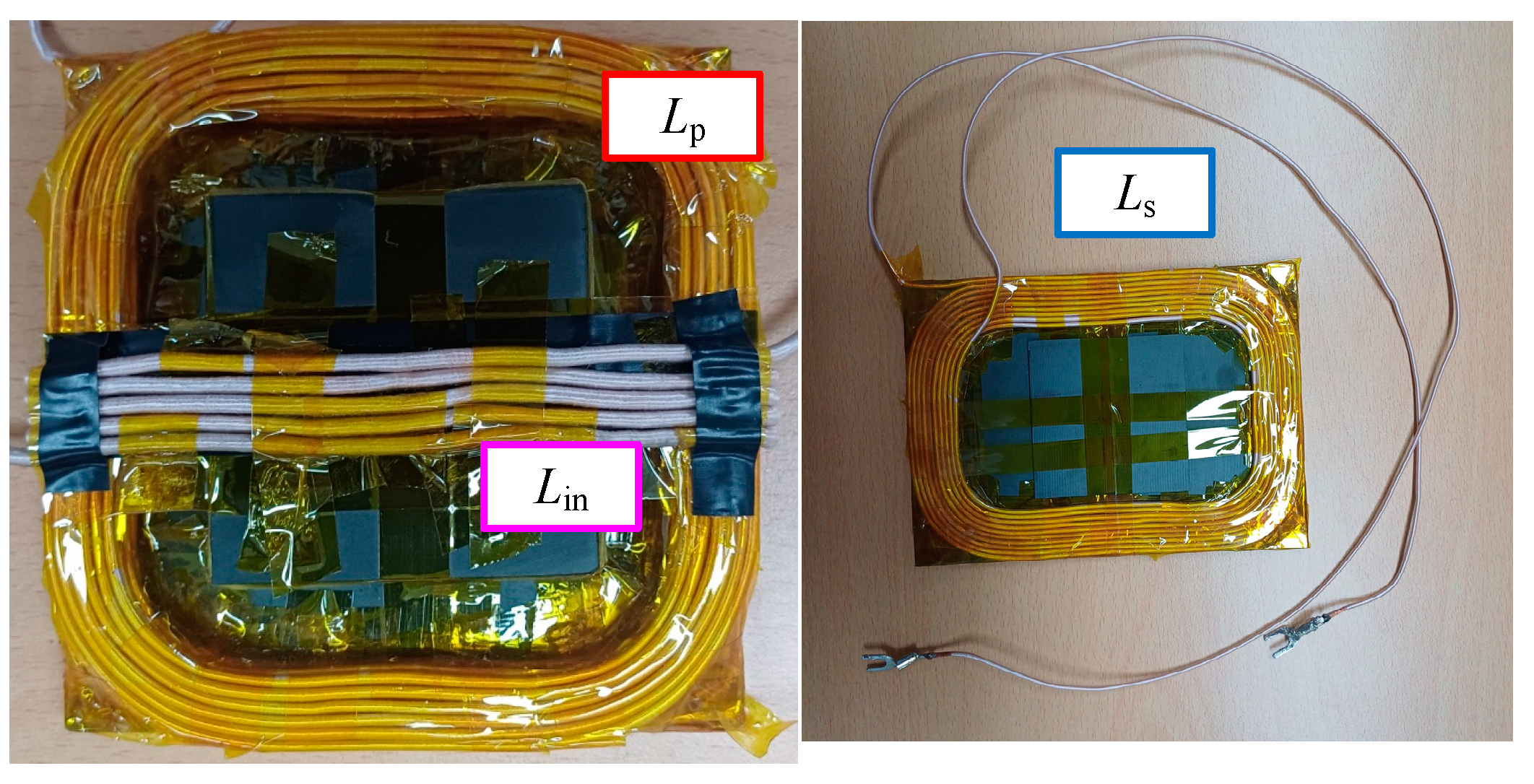
After selecting the wireless pad design, the number of turns and the placement of the magnetic material are determined. The number of turns is selected considering the allowable area of the pad, the inner diameter affecting the
k, and current stress. The diameter of the pad winding is set to 1.5 mm due to
Lp and
k. The current stress is designed to be less than 10 Arms, considering the AWG gauge. The number of winding layers can be as high as six, considering the maximum height of the pad. As the number of turns increases, M increases, which reduces the current required to link the same magnetic flux. However, because the coil winding resistance increases, an appropriate number of turns should be selected considering the losses.
Table 4 shows the magnetic characteristics depending on the number of winding layers of the transmitting pad. The number of turns per layer is fixed at 10, taking into account the inner diameter, and a ferrite magnetic material is added to the center of the pad to increase the coupling coefficient. The receiving pad is fixed at 13 turns in one layer due to the volume limitation of the receiving part.
Table 4 shows that as the number of winding layers increases, the inductance and coupling coefficient increase.
Figure 4 shows the inductance and winding resistance graph depending on the number of winding layers of the transmitting pad. Through
Table 5 and
Figure 4, it can be seen that a mutual inductance of up to 3.369 μH can be achieved (designed), and considering the losses due to winding resistance, it is designed for four layers.
2.3. Selection of the Resonant Networks
When AC flows through the wireless pad, reactance components that impede the current flow are generated. These reactance components increase any reactive current within the IPT system, which leads to higher losses. Therefore, a resonant network is required to compensate for these reactance components. The resonant network can be configured either by connecting capacitors to compensate for the inductance of the primary and secondary pads or by adding more than two resonant elements to obtain a higher-order network [
10]. Commonly used resonant networks are S-S, LCC-S, and DS-LCC topologies [
11,
12,
13].
The design range of
M capable of rated power transmission in the IPT system varies depending on the resonant network configuration.
Figure 5 shows the achievable range of M for the S-S, LCC-S, and DS-LCC topologies. The inverter is assumed to operate at a fixed duty cycle of 0.5 and a fixed operating frequency of 100 kHz. For the S-S topology, the output characteristics are determined by
uin,
M, and
f, which leads to a highly restricted designable
M range. Conversely, the LCC-S and DS-LCC topologies have their output characteristics determined by primary or secondary LC resonant tanks. Moreover, the current flowing through the primary pad is determined by the primary LC resonant tank, while the output-side current is determined by the secondary LC tank. Consequently, as higher-order networks are configured, the range of designable
M that can meet the rating is increased.
Figure 5 shows that the designable minimum
M for the S-S topology is 9.46 μH, which indicates it is not suitable for the system developed in this study. For the LCC-S and DS-LCC topologies, provided the resonant inductor does not exceed the pad inductor in size, the achievable ranges for designable
M are up to 61.9 μH and 458.9 μH, respectively. This demonstrates the feasibility of the targeted system design in this study. Although the DS-LCC topology has the advantage of optimizing losses generated in the pad, it also has the disadvantage of increased losses and reduced power density due to the higher number of passive components. Considering the limited volume of the secondary system designed in this paper, the LCC-S resonant network is selected.
The LCC-S topology consists of a resonant network with one resonant inductor (
Lin) and two resonant capacitors (
Cp,
Cf) on the primary side and one series resonant capacitor (
Cs) on the secondary side. Kirchhoff’s current law for the IPT converter leads to the following equation [
14]:
Through Equation (4), it can be confirmed that the LCC-S topology exhibits constant current characteristics on the primary pad and constant voltage characteristics at the output. The resonant condition for the LCC-S topology can be formulated as follows:
2.4. Selection of the Inverter/Rectifier Structure
When designing a resonant network, it is critical to consider the AC input and output characteristics. Selecting the appropriate inverter and rectifier structures is important, as the output transformation of the IPT converter depends on these properties. Converting the input DC to AC through an inverter or transforming the AC output to DC through a rectifier can significantly alter the gain characteristics. These changes in gain characteristics directly impact the passive components of the resonant network within the IPT system.
In other words, selecting the inverter and rectifier structures is a fundamental step in the design process of the resonant network. Different structures provide different electrical characteristics and efficiencies, which affect the overall performance of the IPT converter. Moreover, the passive elements of the resonant network must be adjusted to match the specific gain characteristics introduced by these components. Hence, determining the optimal inverter and rectifier configuration is key to ensuring that the IPT converter operates efficiently and meets the desired specifications.
For the LCC-S topology, the impact of the inverter’s output gain is minimized because the primary LC resonant filter performs a V-C conversion, thus having little effect on the output characteristics. Given that fewer MOSFET switches in the inverter are advantageous in terms of cost and power density, a half-bridge inverter structure is selected for this study.
Conversely, the rectifier structure directly alters the electrical characteristics as it is connected in series with the secondary pad. When the rectifier is configured as a half-bridge, it operates as a voltage doubler, which increases the current flowing through the secondary pad while it decreases the current in the primary pad. In addition, because the primary pad resistance exceeds the secondary pad resistance, selecting a half-bridge rectifier structure helps improve efficiency and increase power density. Therefore, both the inverter and rectifier structures are chosen as half-bridge configurations.
Figure 6 shows the IPT system composed of a half-bridge inverter, LCC-S topology, and half-bridge rectifier structure based on
Section 2.3 and
Section 2.4.
2.5. Integrated Inductor Design
The
Lin included in the LCC-S topology can be integrated into the primary pad using an integrated coil structure, which reduces both volume and cost [
15].
Figure 7 shows the AC equivalent circuit of the LCC-S topology with the integrated coil. In addition to the primary and secondary pads shown in
Figure 2, the flux linkage generated in the resonant inductor can also affect the primary and secondary pads. If there is a
k between the
Lin and the pads, it can impact both the output characteristics and resonant conditions. Therefore, designing the system to decouple the integrated coil from the pads can be considered. To enable complete decoupling, the coil structure can be configured to cancel out the magnetic flux.
Figure 8 shows a structure where
Lp and
Lin are perpendicular, resulting in canceled total magnetic flux.
The FEM simulation results in
Figure 8 show that
Minp, the mutual inductance between
Lin and
Lp, and
Mins, the mutual inductance between
Lin and
Ls, are nearly zero, indicating that the mutual inductance can be neglected. Based on the pad characteristics in
Figure 8, the system specifications are configured as shown in
Table 5.
Figure 9 shows the PSIM simulation results when applying the pad from
Figure 8 and the system specifications from
Table 5.
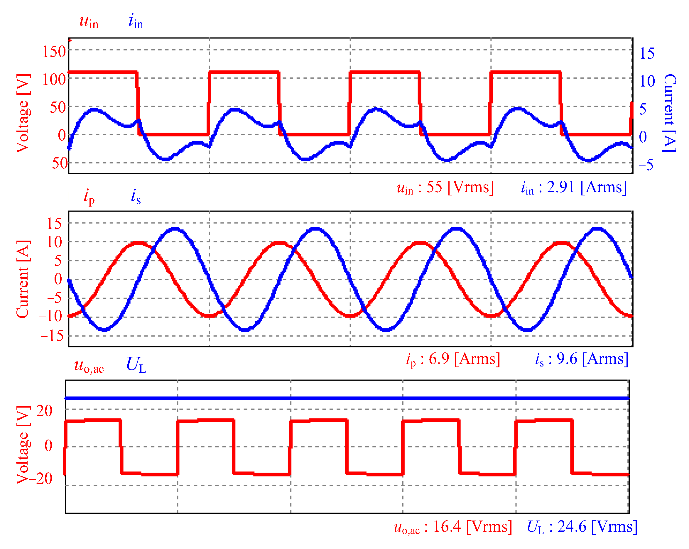
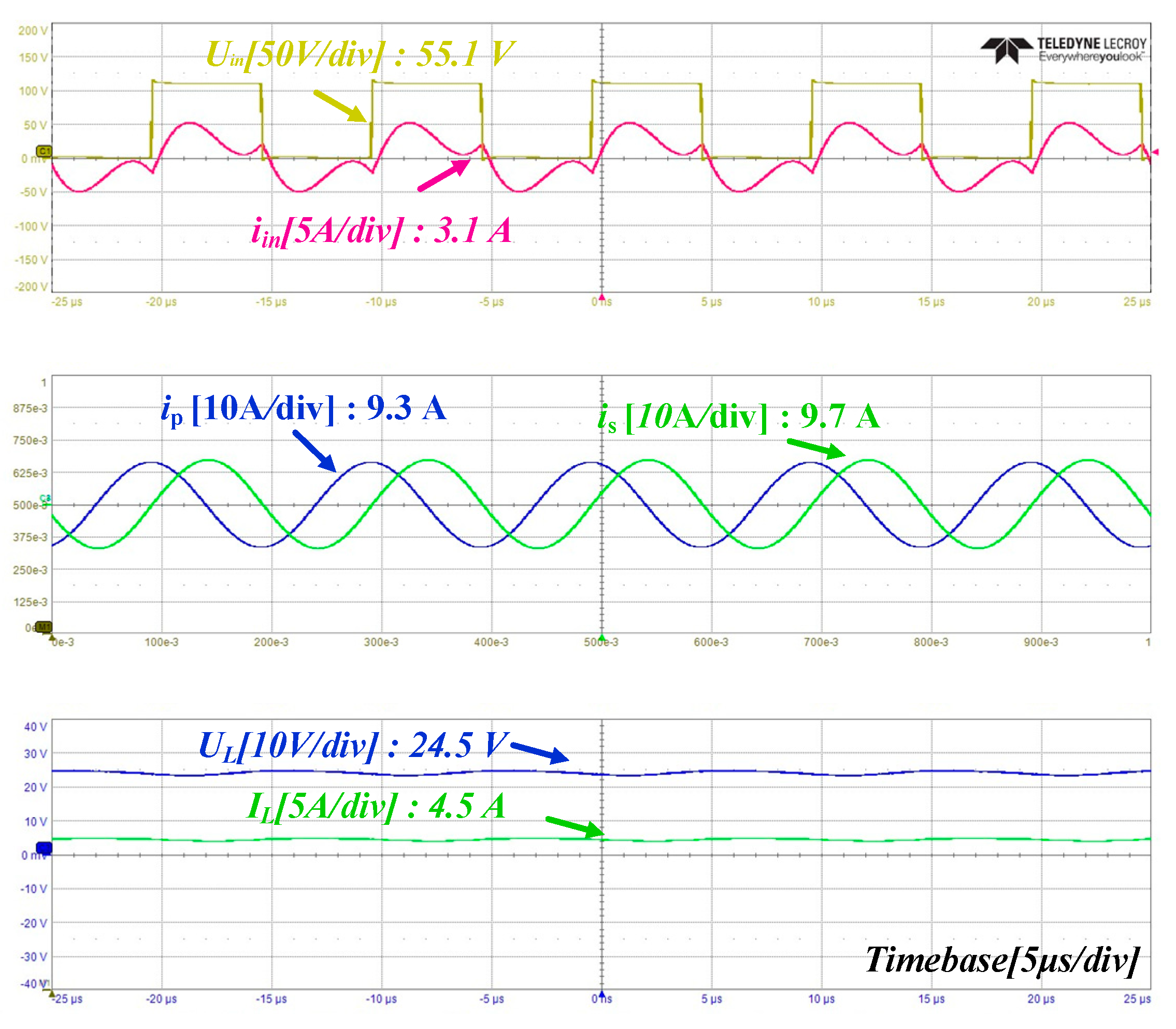
Figure 9 confirms that the proposed system configuration achieves zero voltage switching (ZVS) and rated output characteristics.
Figure 10 shows the FEM simulation results when applying the system specifications from
Table 6. The maximum flux density is 94.7 mT, which suggests that the magnetic material of the primary pad with the integrated coil structure does not saturate.


