1. Introduction
A gallium nitride (GaN) semiconductor is a material with a high energy bandgap compared with conventional silicon (Si) semiconductors. Therefore, it possesses a high breakdown voltage and excellent electron mobility characteristics, resulting in high power density at high frequencies. Additionally, it boasts resistance to high pressure and temperature, rapid signal conversion speed, and high efficiency [
1]. These attributes have garnered it attention as a next-generation power semiconductor, and its commercialization is rapidly advancing, particularly in smartphone fast chargers, 5G/6G mobile communications, and electric vehicle power systems. According to a recent forecast by the market research firm Yole Development, the global GaN power semiconductor market is expected to grow from USD 185 million in 2022 to USD 2.035 billion by 2028, representing a compound annual growth rate (CAGR) of 49% [
2].
GaN semiconductor devices, especially GaN high-electron-mobility transistor (HEMT) devices, known for their excellent electron mobility characteristics, have seen widespread adoption in high-frequency integrated circuits for transmitting and receiving. These circuits can operate stably at high frequencies and handle high power, meeting the increasing demands of radio and telecommunication applications. Active research in this field is ongoing [
3,
4,
5]. In particular, GaN semiconductor devices are emerging as the sole high-frequency power semiconductors suitable for use in semiconductor-based solid-state power amplifiers (SSPAs), replacing the vacuum tube-type traveling wave tube amplifiers (TWTAs) traditionally used in military applications [
6,
7].
With advancements in semiconductor process technology, high-frequency circuits for wireless communication have been integrated and miniaturized using monolithic microwave-integrated circuits (MMICs). GaN HEMT MMICs have been widely studied as high-power, broadband power amplifiers due to their advantage of high power density at high frequencies [
4,
5,
6].
Millimeter-wave (mmWave) high-power, high-efficiency GaN power amplifiers are in high demand for satellite communications and military applications. MmWave high-output power amplifiers have been applied to GaN HEMT MMICs, and output power (P
out) results as high as 40 W in the Ka band have been recently reported [
8]. It was designed using undisclosed internal semiconductor processes from Japan and the U.S. and was based on parallel power combining of commonly used output-stage transistors. However, this has been limited to the lower Ka band (defined as 33 GHz or lower), and output power results of 10 W or more in the upper Ka band (defined as 33 GHz or higher) have been published in several papers [
9,
10,
11,
12,
13]. Ref. [
9] demonstrated over 10 W of P
out using GaN HEMTs with a power density of 5 W/mm at 35 GHz on SiC substrates, known for their excellent thermal conductivity. Ref. [
10] also achieved 9 W of P
out and an outstanding power-added efficiency (PAE) up to 33% in the upper Ka band using SiC substrates. Ref. [
12] attained more than 10 W of P
out in the 18–40 GHz wideband by utilizing a combination of distributed amplifier and reactive matching topology, which are two common wideband design techniques. These studies focused on high-power amplifiers (HPAs) implemented with GaN-on-SiC technology. Recently, GaN high-power amplifier (HPA) MMICs using GaN-on-Si technology, which can be fabricated on the same substrate as conventional integrated circuits and offer cost competitiveness, have also been actively studied [
13].
In this work, we design and implement an mmWave high-power GaN power amplifier (PA) MMIC for future satellite communication applications. Additionally, as mentioned above, GaN-on-Si has significant potential and advantages, so we design our MMIC using this process. In particular, the upper Ka band, which has relatively few design examples among the Ka bands, is selected as the operating frequency, and the design process is systematically summarized.
Figure 1 illustrates the design process of the mmWave GaN PA MMIC in this study. Initially, the MMIC’s specifications are determined based on the intended application. For a power amplifier MMIC, typical specifications include saturation output power (P
sat), power-added efficiency (PAE), power gain, and chip size. Subsequently, load pull simulation of GaN HEMTs is conducted to determine the optimal transistor size that meets the specifications. Particularly at high frequencies, above 30 GHz, electromagnetic (EM) verification of the source via structure holds significant importance in the design of GaN HEMT power amplifiers. Given that load pull results are strongly influenced by the source via model at such frequencies, more accurate predictions based on EM are crucial. Once the optimal GaN HEMT size is determined through load pull simulation, the power stage and drive stage are designed to fulfill the input and output power requirements. This involves determining the number of stages needed for the total power amplifier. Subsequently, schematic-level MMIC design and layout are executed using the design kit provided by the foundry. To enhance the realism of simulation results, partial EM simulation is conducted during layout to validate the layout structure’s proximity to schematic simulation. Finally, a full EM simulation is performed on the entire layout to ensure satisfaction with specifications before tape-out.
This paper is organized as follows: In
Section 2, the above-mentioned mmWave GaN PA MMIC design process will be described in detail in sequence and simulation results will be presented. In
Section 3, the designed PA is fabricated using a commercial process and the measurement results are presented, followed by conclusions in
Section 4.
2. Circuit Design
In this study, we set the goal of designing an MMIC with an average output power over 8 W in the upper Ka band. Additional specifications include a power gain of more than 10 dB and a PAE of more than 10%. The design of a Ka-band PA MMIC to meet these specifications is accomplished as follows.
2.1. Load Pull Simulation
The output power from a transistor depends on the load impedance. Load pull is an essential process in power amplifier design, where the output power or power efficiency of the transistor used is investigated as a function of the load impedance at a given operating frequency and bias. At low frequencies, load pull data can be obtained through measurement by connecting an impedance tuner to the transistor to be used. However, at high frequencies above millimeter waves, the equipment setup is difficult, and the measurement error is large. Therefore, it is common to perform load pull simulation using an accurate large-signal model.
RF power is proportional to RF current and RF voltage. Therefore, if the driving voltage remains constant, the larger the size of the transistor, the greater the output power. However, as the transistor size increases, so does the parasitic capacitance. This leads to increased mismatch between current and voltage swings at high frequencies, as well as higher DC power consumption. As the size increases beyond a certain point, the incremental gains in output power diminish, leading to a decline in efficiency. Additionally, surpassing a specific threshold in transistor size leads to a decrease in high-frequency linear gain due to parasitic capacitance. This necessitates higher input power in power amplifier design. Hence, selecting the optimal GaN HEMT size requires consideration of these factors.
In this design, GaN HEMT devices with a maximum available gain (MAG) or maximum stable gain (MSG) of at least 10 dB in the Ka band, prior to load pull analysis, are chosen as the primary candidates.
Figure 2a,b show the simulated MAG and stability factor according to the size of GaN HEMTs. Depending on the gate fingers and gate widths provided by the foundry, the simulated GaN HEMT devices with the largest sizes while satisfying an MAG or MSG of more than 10 dB are 6 (hereafter gate finger) × 70 (hereafter gate width) μm, 6 × 100 μm, 8 × 70 μm, and 8 × 100 μm, as shown in
Figure 2a. When compared with the same unit gate width, the device with six gate fingers had a higher MAG of about 2 dB compared to the device with eight gate fingers.
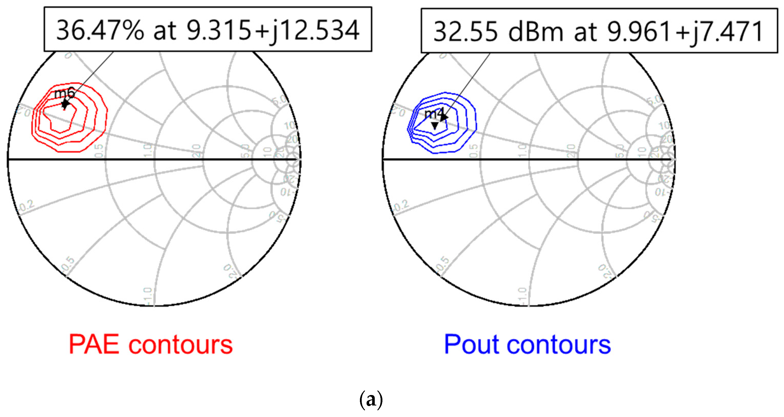
Load pull simulations were performed on these four transistors. First, we set the input impedance to 50 ohms and used the impedance tuner to vary the load impedance value to find the load impedance that produced the maximum output power, then performed a source pull on the input side to find the source impedance that produced the maximum output power again. Finally, with the optimal source impedance set, load pull was performed again to determine the final load impedance.
Figure 3a–d show the GaN HEMT load pull simulation results for different sizes, respectively. The drain voltage is set to 12 V and the gate voltage is set to −1 V, referring to the foundry-provided model guide document. The frequency is set to a single frequency in the Ka band and the input power is set to 25 dBm.
As shown in
Figure 3a–d, the 8 × 70 μm GaN HEMT exhibited the highest PAE of about 38%, while the 8 × 100 μm device had the highest output power of about 33.4 dBm. The optimal load impedance values are 9 to 10 ohms for the 6 × 70 μm device and 5 to 6 ohms for the rest of the devices for the real part. The 8 × 100 μm GaN HEMT exhibits high output power, but its maximum PAE is approximately 32%, which is more than 4% lower than that of the other devices. Therefore, the 8 × 70 μm GaN HEMT, which offers the highest PAE and a modest 0.4 dB difference in output power, is selected as the unit cell transistor for the power amplifier.
2.2. Source via Effect Consideration
Because GaN HEMTs are highly self-heating due to their high power density, they often use ground-source via structures to dissipate the generated heat to the outside [
14].
Figure 4 shows the GaN HEMT common source layout and the three-dimensional structure of the source via holes used in it. As shown in
Figure 4, the source via hole is modeled as an inductance because it connects the source terminal to the ground with a hole about 100 μm thick, and the inductance value can vary with frequency, which needs to be verified by EM simulation. Larger inductance values reduce the maximum output power and maximum possible efficiency at high frequencies when performing load pull. To account for this, it is recommended to increase the width of the source via as much as possible, but the width should be adjusted appropriately so that it does not interfere with the layout of other circuits. In this design, a 200 µm wide ground via hole is used as the source via hole.
GaN HEMTs, characterized by high power density, often employ ground-source via structures to dissipate generated heat.
Figure 4 illustrates the common source layout of GaN HEMTs along with the three-dimensional structure of the source via holes. These holes, approximately 100 µm thick, act as channels linking the source terminal to the ground and are represented as inductors in modeling. The inductance value is frequency-dependent, necessitating verification through EM simulation.
Higher inductance values may restrict maximum output power and efficiency at high frequencies during load pull. Therefore, widening the source via is recommended, ensuring it does not interfere with the layout of other circuits. In this design, a 200 µm wide ground via hole is utilized as the source via.
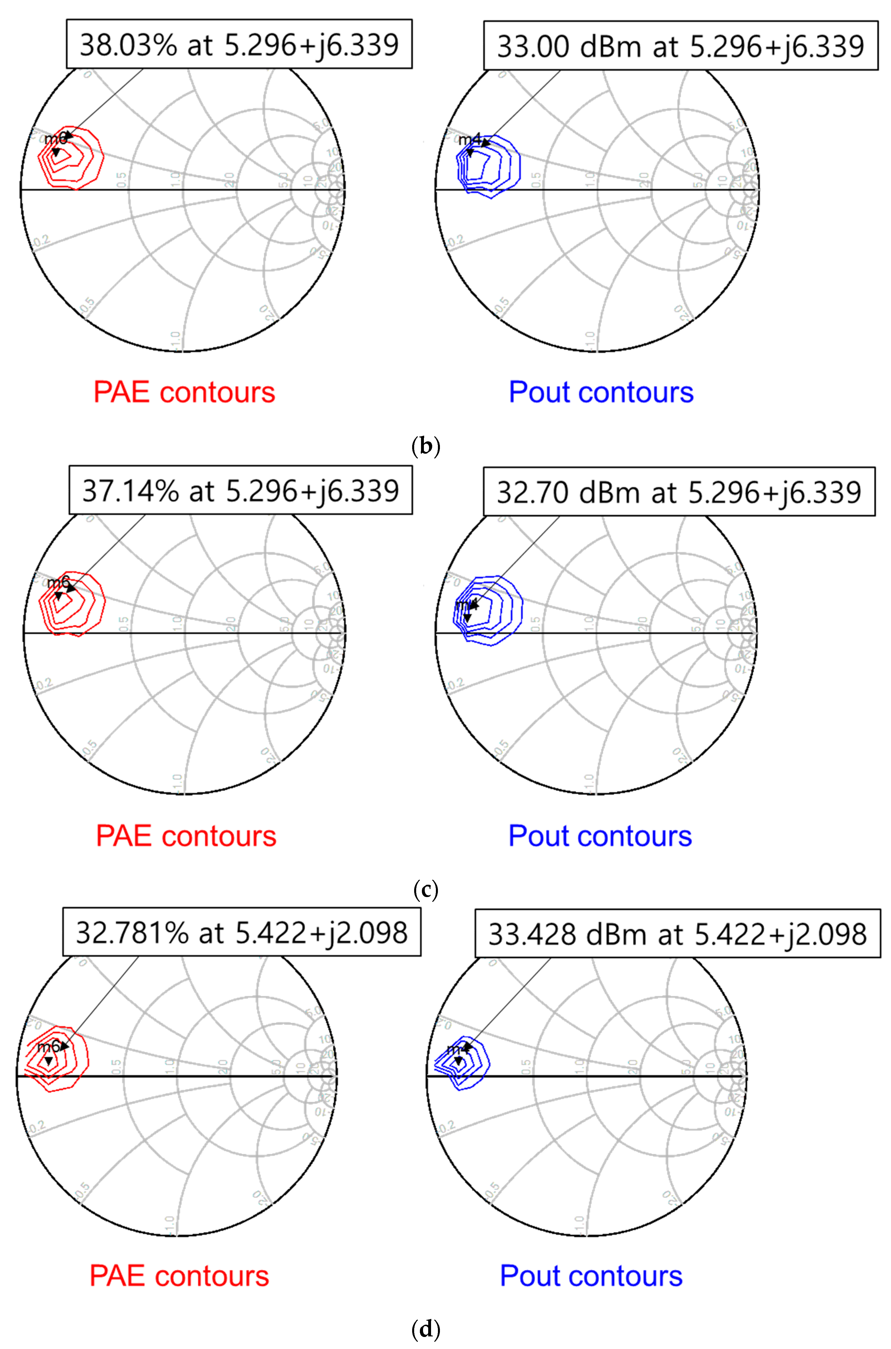
Figure 5 compares the design kit model of the ground via hole, provided by the foundry, with EM simulation results obtained from the same device layout. The EM verification reveals an additional phase increase of approximately 8 degrees in the upper Ka band. This corresponds to an inductance of about 15 pH at that frequency.
Figure 6a,b demonstrate the variation in load pull P
out and PAE depending on the source ground model. As shown in
Figure 6a,b, the P
out and PAE progressively deteriorate as the source ground moves away from the ideal ground and closer to the EM data-based via-hole model that reflects the actual layout. Particularly in
Figure 6a, a noticeable reduction in P
out, exceeding 1.3 dB, is observed when the source ground via-hole model given from the foundry design kit incorporates additional inductance consistent with EM simulation results. Consequently, the overall system budget to meet specifications must include allowances for the reduction in maximum P
out due to parasitic inductance introduced by the source via holes.
2.3. Unit Power Cell Schematic Design and System Budget Calculation
After determining the appropriate sizing of the GaN HEMT for the unit power cell based on the earlier load pull simulation results, the single-stage PA is designed using the practical design kit. Initially, for simplicity in design, the matching circuit can be conceptualized as an ideal passive element and later substituted with the actual passive element model from the design kit.
While the load impedance circuit remains consistent, the approach to implementing the input impedance matching circuit varies. To achieve a source impedance of 50 ohms on the Smith chart, two different structures can be utilized for the input matching circuit.
Figure 7a,b illustrate the schematics for each structure:
Figure 7a presents the input matching as a shunt L–series C–shunt L–series C structure, while
Figure 7b depicts the input matching as a shunt C–series L structure. However, in this case, the stability at low frequencies is poor; a series R–C circuit is added with an additional dc block capacitor.
Figure 8a,b present a comparison of simulated S-parameters, P
out, and PAE based on different input matching structures. When using the design kit model with losses, the simulated P
out results indicate a reduction of over 1 dB compared to the load pull simulation. As depicted in
Figure 8a,b, the simulation comparison reveals that the shunt C–series L structure exhibits broader S21 and P
out characteristics due to its single resonance structure and the incorporation of an R–C stabilization circuit. Conversely, the shunt L–series C–shunt L–series C structure demonstrates relatively narrower S21 and P
out characteristics owing to its double resonance, which distributes S21 across two frequencies. Increasing the stage number of the amplifier to achieve higher gain further reduces the bandwidth, so a unit cell design with a higher bandwidth is more favorable under the same conditions. Thus, the shunt C–series L structure is selected as the unit power cell design for this study.
Based on the unit power cell simulation results outlined above, the system budget is calculated, taking into account the maximum available input power and the minimum required output power. The entire power amplifier stage is then configured as shown in
Figure 9. As shown in
Figure 9, assuming the input power available is up to 25 dBm and the required minimum of 39 dBm, a minimum of three stages are required. The first stage focuses on achieving high gain with two unit power cells, the second stage focuses on driving the output power with four unit power cells, and the third stage focuses on achieving maximum output power through power combining with eight unit power cells.
2.4. MMIC Schematic Design
A three-stage power amplifier is designed based on the single power cell designed earlier and the calculated system budget. The input and output ports of each stage are designed to be 50 ohms, but the inter-stage matching can be optimized with proper tuning to account for the total chip size.
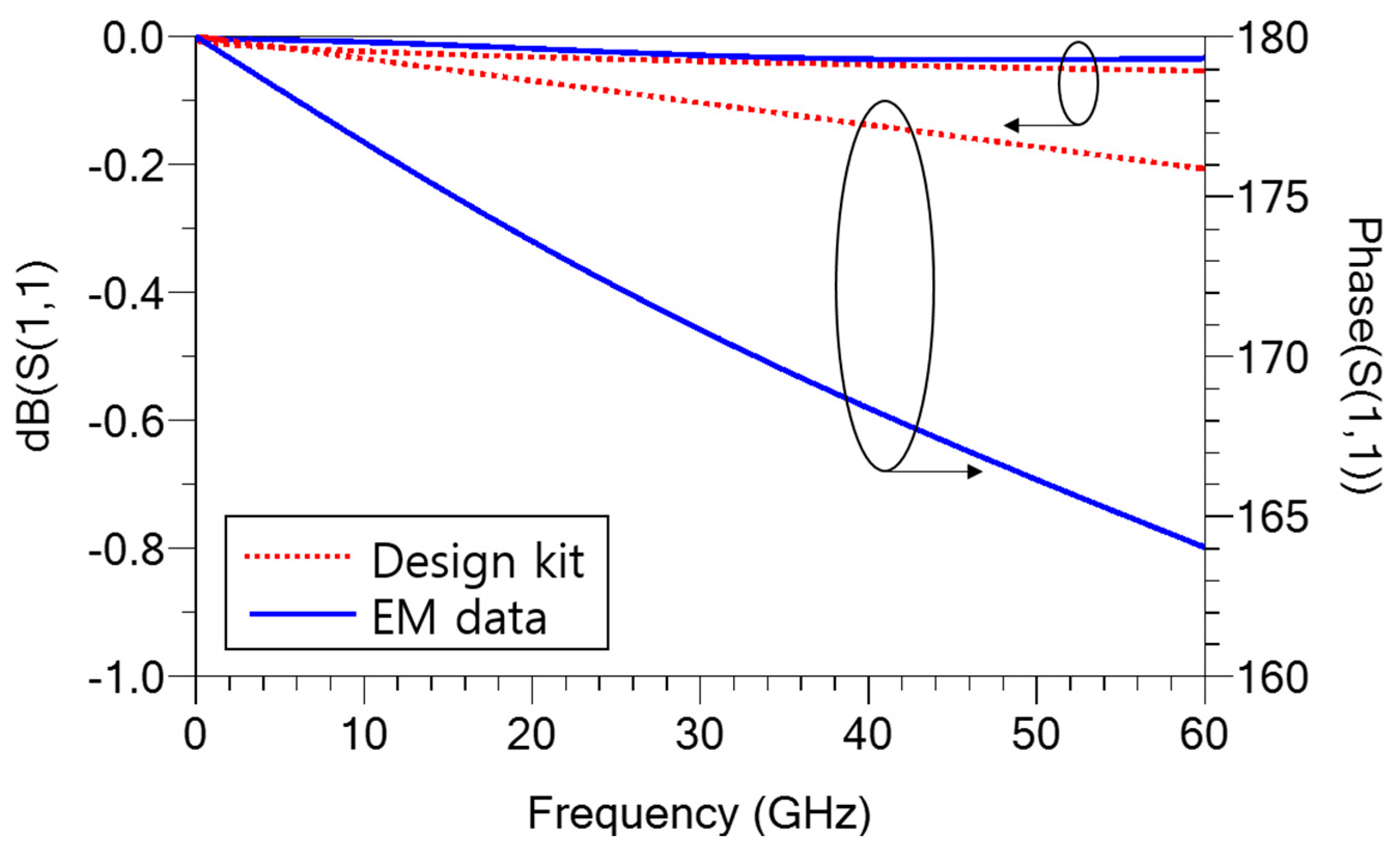
In the power stage design, to simplify the bias circuitry, we implement an output matching circuit for each power cell, tying them together in the primary and laying out the drain bias circuit to be common to all four power cells. This changes the output impedance matching circuit of power cells and puts a shunt capacitor in the middle of the inductive lines. Via holes are required to connect shunt capacitors to ground, which introduce parasitic inductances that are not negligible in the mmWaves. The schematic variation from the initial load-matching circuit to a load-matching circuit that takes into account the layout for parallel power combining and via-hole inductance is illustrated in
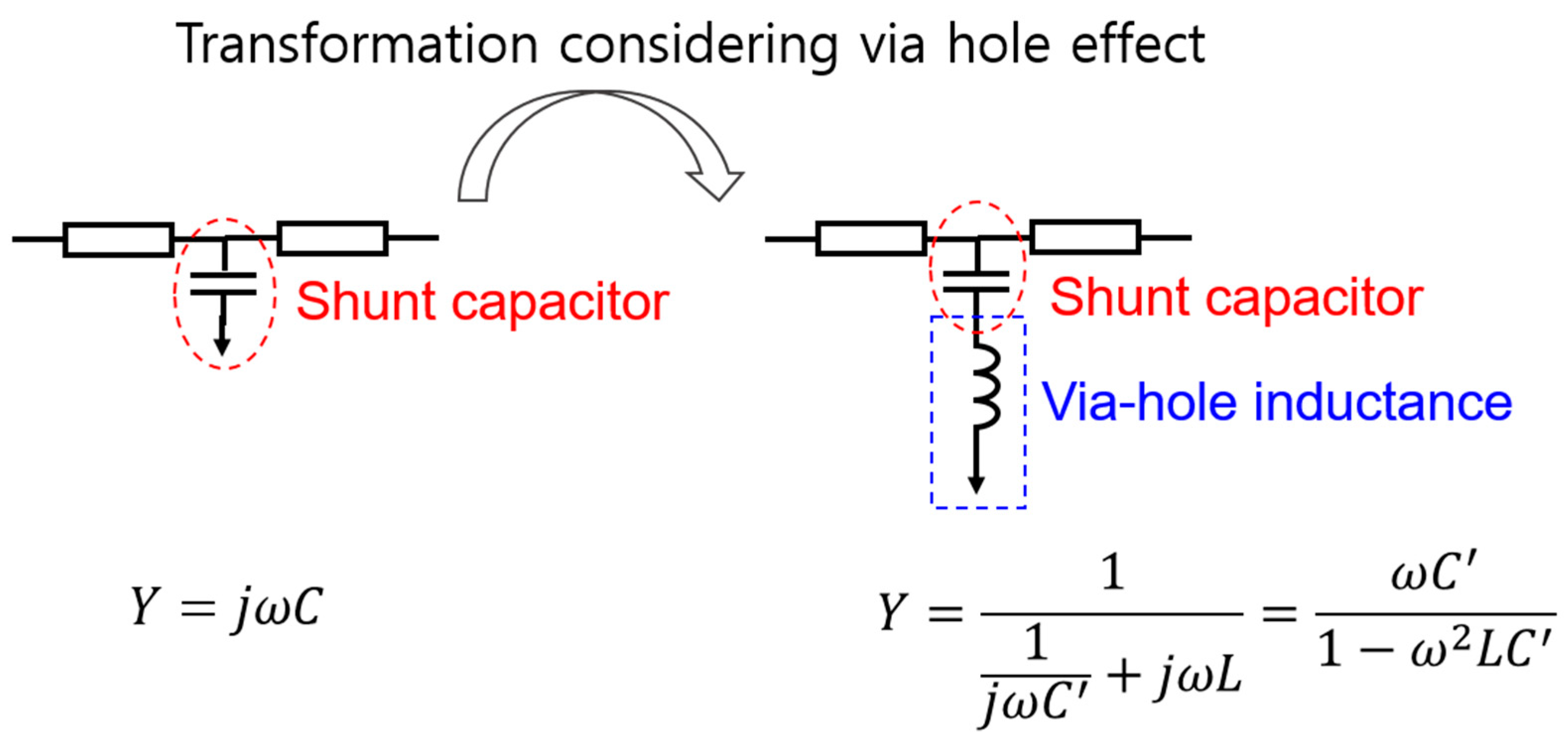
Figure 10. In this work, the inductance of the via hole is extracted based on EM, and the admittance when connected to the shunt capacitor is calculated and compared with the admittance of the shunt capacitor and ideal ground structure, and the equivalent capacitance could be designed to have the same admittance value.
Figure 11 shows the transformation of the admittance when the inductance due to via holes is taken into account, where
C and
C′ are the original shunt capacitance and the modified shunt capacitance,
L is via-hole inductance, and ω is angular frequency.
From Equations (1) and (2), as the value of
L is added, the value of
C′ will be smaller than that of
C. Therefore, the via-hole inductance can be extracted by EM and the proper shunt
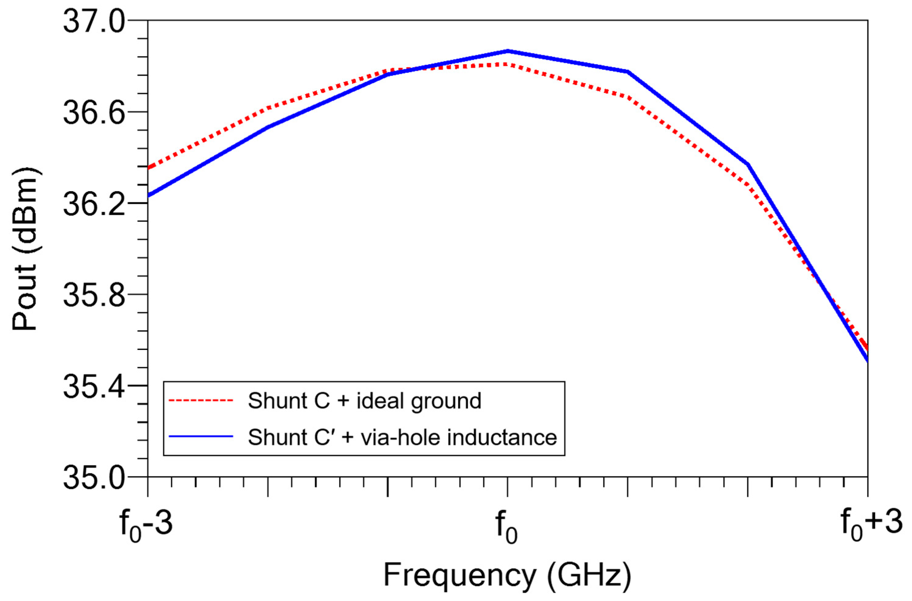
C value can be found. The ground via-hole size for shunt
C for load matching is 50 μm, which is chosen considering the minimum separation distance from the source via hole of the neighboring transistors. In this case, the inductance value extracted from EM simulation is approximately 45 pH. Originally, the shunt capacitance is 150 fF assuming an ideal ground, but the shunt capacitance is reduced to 120 fF after considering the via-hole inductance. In this case, the simulated comparison of P
out for the parallel power combining of the four power cells between ideal ground and via-hole inductance in the load-matching circuit is shown in
Figure 12. As shown in
Figure 12, the output power is not reduced in the upper Ka band and the load-matching circuit is well converted.
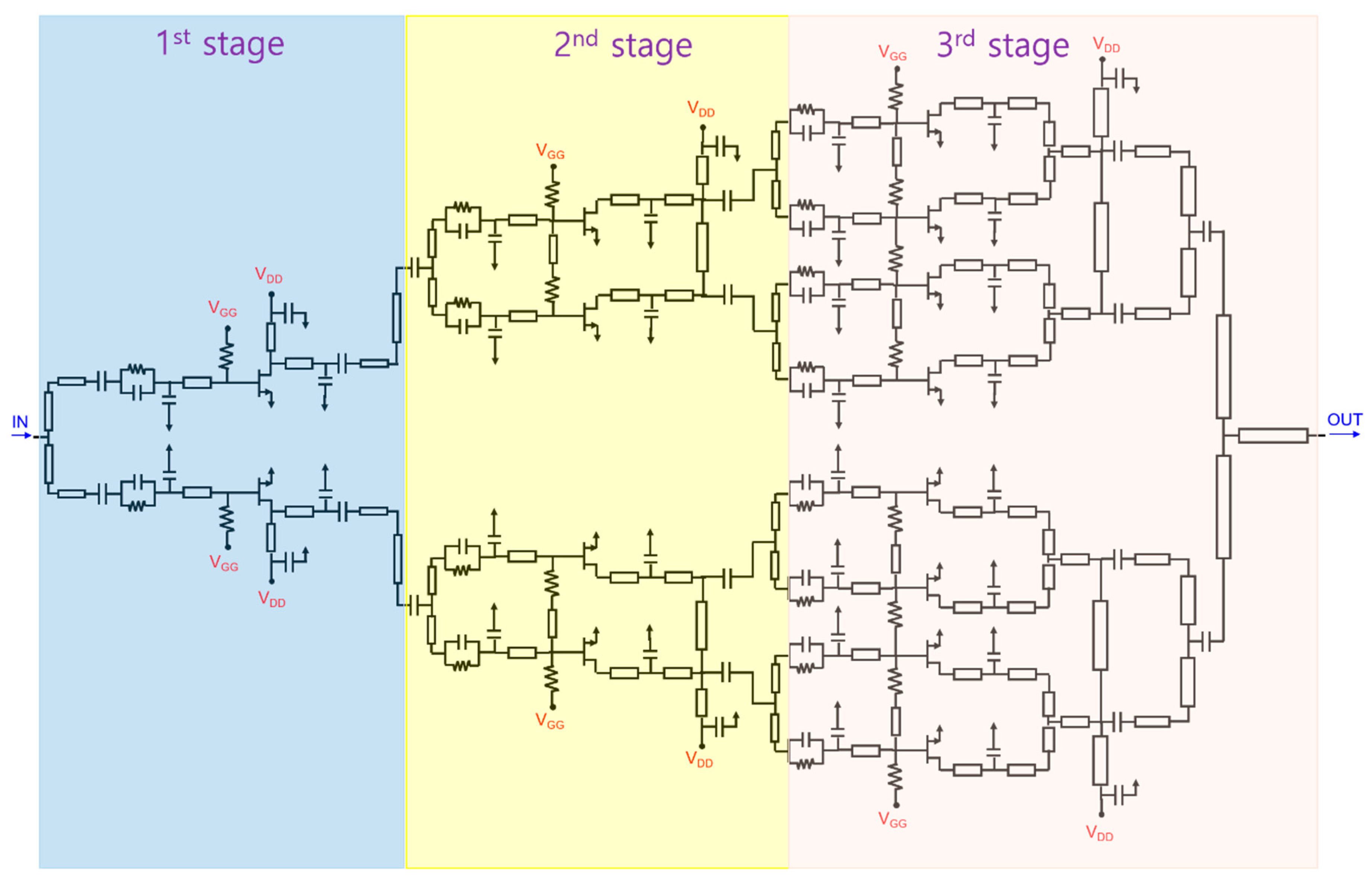
Figure 13 shows the schematic of the complete power amplifier MMIC. The GaN HEMTs used in each stage are identical at 8 × 70 μm, and each stage is symmetrical on the upper and lower sides. The second and third stages are designed to bundle the gate bias lines and drain bias lines of the power cells for convenient bias supply. The line length is minimized to reduce the influence on the input–output matching as much as possible. However, the line thickness is designed considering the current allowance range for the drain bias line.
Figure 14a,b show the simulation results of the entire power amplifier MMIC designed at the schematic level. The bias condition is V
DD = 12 V and V
GG = −1.45 V.
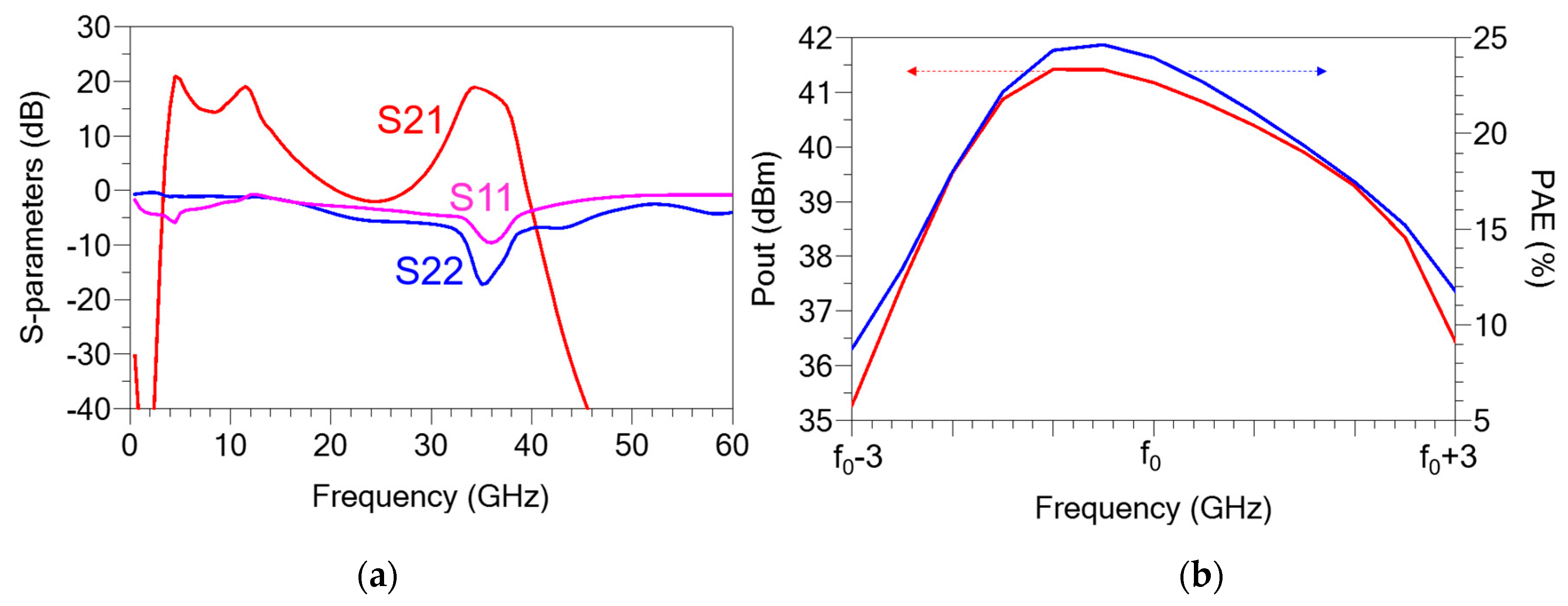
Figure 14a shows the small-signal S-parameter simulation results, showing S21 of approximately 16 to 19 dB at frequencies of the upper Ka band, while S11 and S22 are designed to obtain values below −15 dB, with S11 being frequency-shifted up to minimize gain reduction at high edge frequencies.
Figure 14b shows the harmonic balance simulation result at a single frequency in the Ka band, showing a saturated P
out of about 40.7 dBm and a PAE of 25%.
2.5. MMIC Layout and EM Verification
After the schematic design, the MMIC layout for chip fabrication should be made to reflect the schematic, and EM verification is finally performed to validate the performance of the chip layout. As the layout progresses through the stages, partial EM simulations are performed to tune and optimize the layout similarly to the simulation results performed at the schematic level. Typically, EM simulation results may degrade due to coupling or radiation effects that are not accounted for in the schematic. Therefore, it is important to layout the design in a way that minimizes these issues. In addition, odd mode oscillation is an important consideration in the layout of power amplifier MMICs. When a power amplifier operates, large input and output signals are passed through the circuit, and if the power-combined power cells are not exactly symmetrical, the RF signal is directed to one side, which can damage transistors or cause them to fail. To prevent this odd mode oscillation from occurring, the layout must be exactly symmetrical to ensure that the RF signal is uniformly passed through each power cell, and large shunt resistors can be added to the gate or drain side of the transistor to block or absorb the oscillation if it occurs.
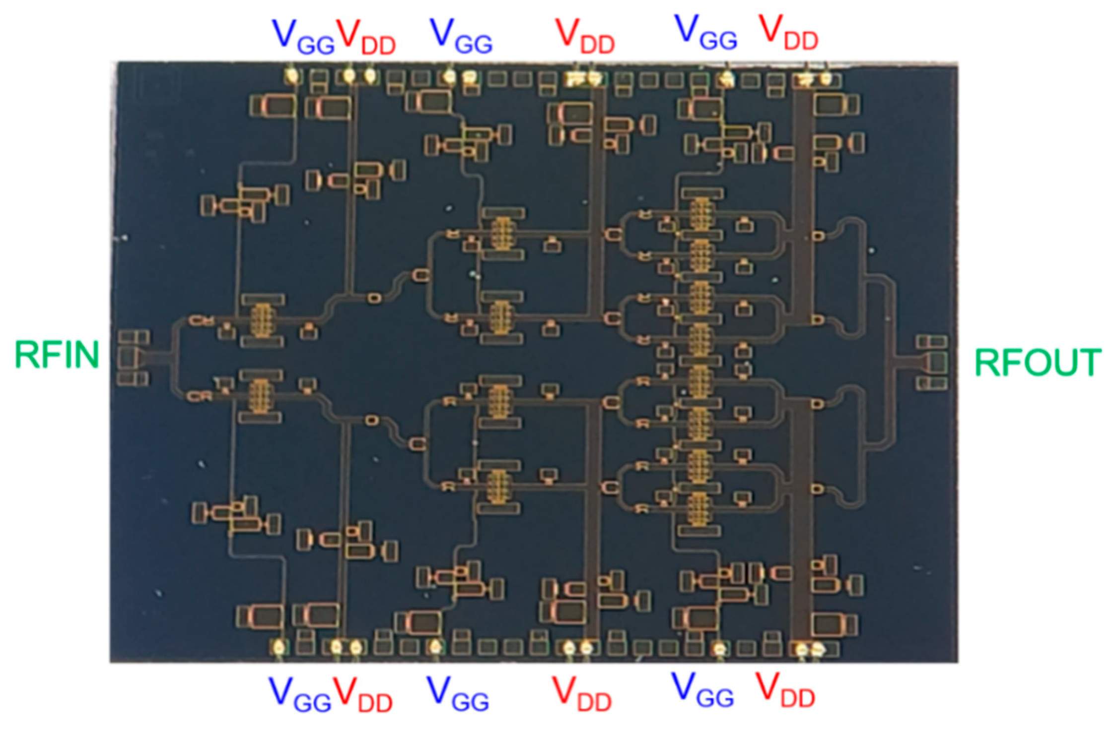
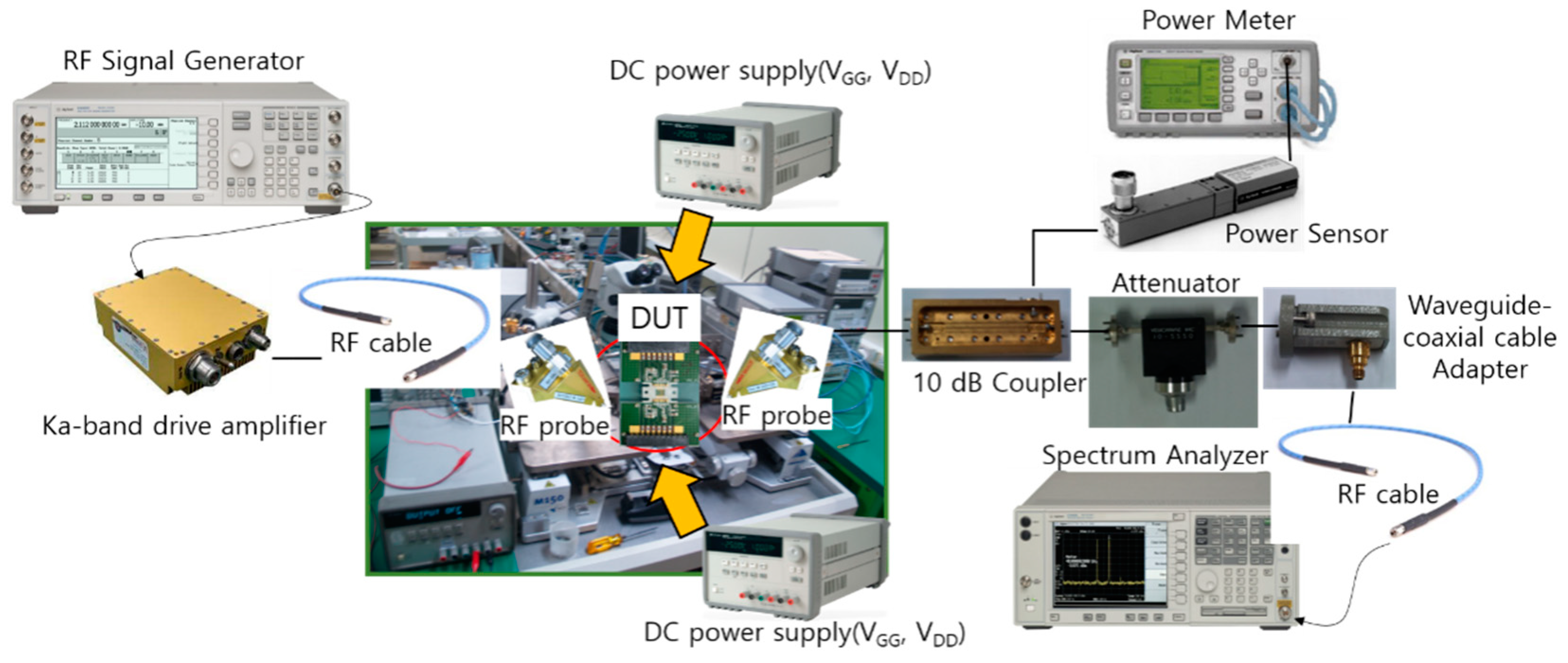
Figure 15a shows the final layout of the three-stage power amplifier MMIC. To achieve a compact chip size, the GaN HEMTs in the power stage are power-combined by sharing the source via ground. The top-to-bottom layout is symmetrical to prevent odd mode oscillations, and partial verification is performed with EM simulations. Finally, a full EM verification of the entire chip is performed. The EM tool used is Keysight’s ADS 2022 Momentum.
Figure 15b shows the EM structure with the ports set up, except for the transistors, to perform the full EM simulation, and
Figure 16a,b show the simulation results after full EM verification.
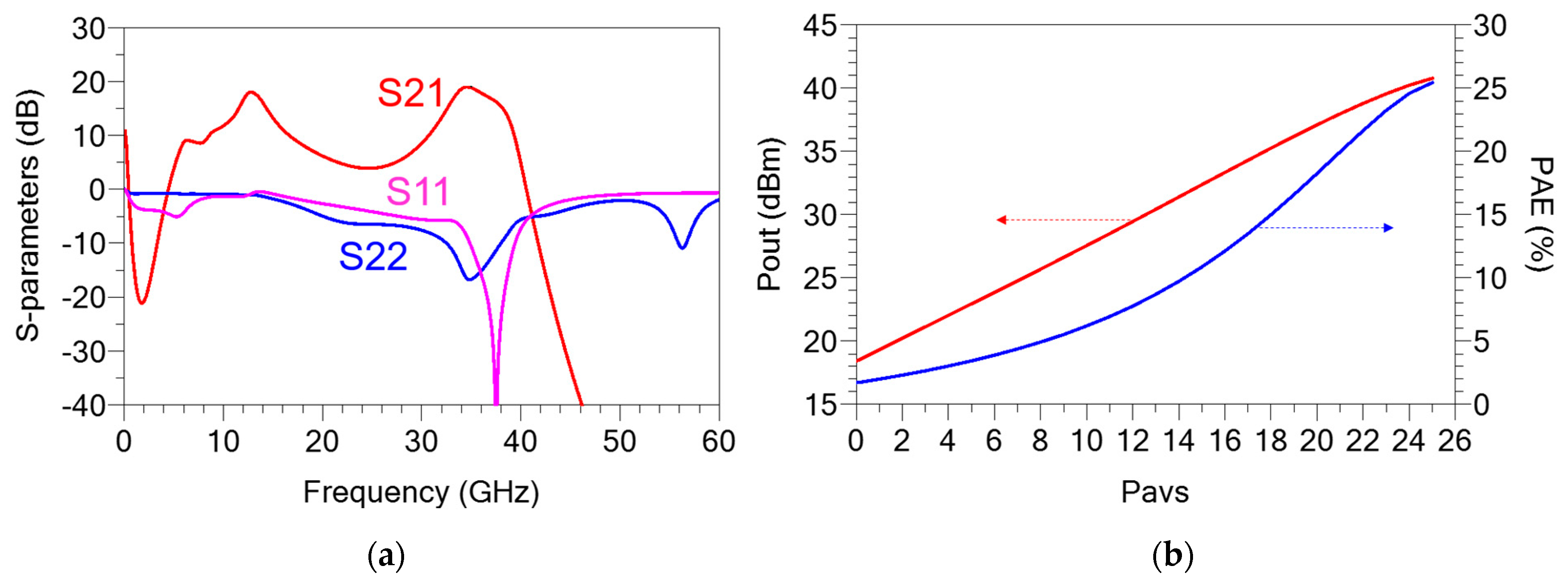
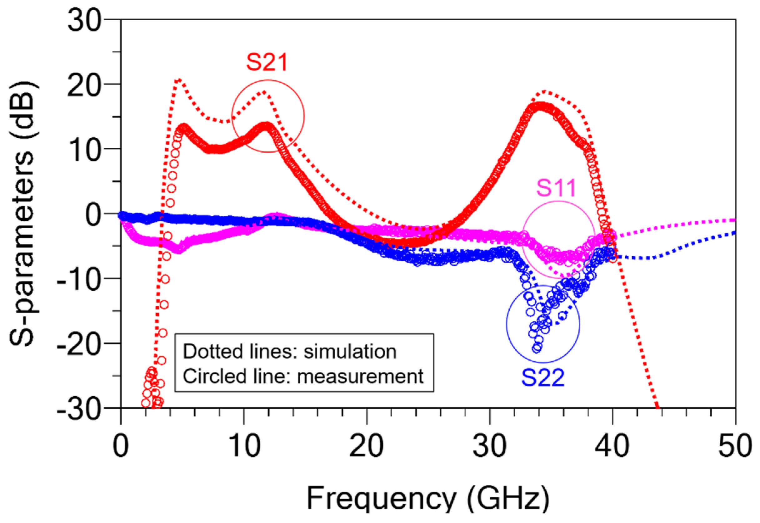
As shown in
Figure 16a, the full EM-based simulation represents an S21 characteristic similar to the schematic level, with a narrower bandwidth and poorer S11 and S22 characteristics.
Figure 16b presents the harmonic balance simulation results as a function of frequency, indicating an output power ranging from 39.3 to 41.4 dBm and a PAE between 17.4% and 24.6%.


