Abstract
PLLs with small areas, low power consumption, and low jitter are crucial for mobile applications. Hence, achieving a balance between the area, power consumption, and noise of a PLL is a significant issue. In this work, a compact, low-power, and low-jitter fractional-N PLL using Ring-VCO is introduced. In order to reduce area and power consumption, a single-ended Ring-VCO is implemented. Additionally, novel resistance matrixes are proposed to decrease phase noise. The resistor matrix creates 13 frequency tuning curves with close VCO gain and different initial frequencies, reducing the VCO gain and thus the overall noise while maintaining high tuning linearity. The proposed PLL is fabricated based on 12 nm FinFET technology with a 0.078 mm2 area. It achieves a 2.702 ps RMS jitter at 5.76 GHz while consuming 6.4 mW. Moreover, it maintains a low power consumption and a low RMS jitter across the entire frequency range.
1. Introduction
Phase-locked loops (PLLs) are essential components in wireless communication systems for generating high-performance clock signals [1,2,3,4]. With the explosive development of mobile applications, there is an increasing demand for highly integrated and low-power-consuming PLLs [5,6,7]. To achieve a smaller area and lower power, digital PLLs have been developed, which offer advantages such as compactness, low power consumption, and high programmability [8,9,10]. However, digital PLLs have longer lock-in time and inferior noise performance compared to analog PLLs [11,12]. In conventional analog PLLs, the low-pass filter (LPF) and the voltage-controlled oscillator (VCO) are the primary contributors to the overall area. On the one hand, the structure of LPFs is simple and closely related to the bandwidth, leading to difficulty in modification. On the other hand, due to the diverse implementation methods of the VCO [13], there is potential to reduce its area.
The LC-VCO shown in Figure 1a is commonly used in conventional analog PLLs, featuring a simple structure and low jitter [14,15,16,17]. In comparison, the Ring-VCO is formed by connecting an odd number of delay units in series, eliminating the need for capacitors and inductors. This results in a smaller area [18,19,20]. Many studies have proposed PLLs based on differential Ring-VCOs, which achieve a compact area and wide tuning range at the expense of increased noise [21,22,23]. Moreover, the area and power of the VCO can be further reduced.
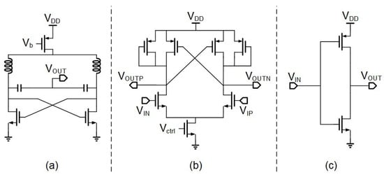
Figure 1.
(a) Oscillation unit in LC-VCO and delay unit in (b) differential Ring-VCO and (c) single-ended Ring-VCO.
Here, for the first time, we propose a single-ended Ring-VCO-based PLL based on the FinFET process. Compared to the delay units of the differential Ring-VCO shown in Figure 1b, the delay units of the single-ended Ring-VCO (Figure 1c) employ fewer devices and require no tail current circuit. In addition, it requires a smaller voltage supply. This enables a smaller area and lower power consumption. In addition, novel resistor matrixes are proposed to construct 13 frequency tuning curves with close VCO gain () and different initial frequencies, which reduces and thus phase noise. The proposed PLL exhibits low complexity, minimal space requirements, and low power consumption, making it highly suitable for mobile RF transceivers. It achieves a small area of 0.078 mm2 and low power of 6.4 mW. Additionally, it attains a maximum output frequency of 6.72 GHz and an RMS jitter of only 2.702 ps.
2. The Design Scheme of the Proposed Ring-VCO
There are three common issues associated with single-ended Ring-VCOs when compared to other types of VCOs: low maximum frequency, poor stability, and low phase noise. In this study, we propose the following solutions.
The single-ended delay unit has low speed and therefore low maximum frequency. And since the current driving capability of FinFETs is much better than MOSFETs, high frequencies can also be achieved using FinFET inverters [24]. Although the use of single-ended delay units reduces the maximum frequency, this problem is compensated by using the FinFET process, which increases the maximum frequency.
The single-ended delay unit is not stable, mainly because it is more susceptible to power supply fluctuations and spatial coupling than the differential delay unit. The solution is to use a stable power supply and protect it with guard rings in the layout.
The single-ended Ring-VCOs have poor phase noise, especially compared to LC-VCOs. So novel variable resistor matrixes are proposed to improve the noise performance by reducing the . A total of 13 frequency tuning curves are created with close and different initial frequencies. Therefore, it is possible to reduce the and hence the overall phase noise of the PLL to an acceptable range.
Since the maximum frequency problem can be solved by process selection, and the stability problem can be solved by stabilizing the power supply and guard rings in the layout, the focus of the following part is on phase noise reduction through circuit improvement.
The output frequency of the VCO can be expressed in the time domain as
where is the VCO gain, is the control voltage of the VCO, and is the initial frequency of the VCO. Integrating both sides of Equation (1) yields the VCO output phase in the time domain, as shown in Equation (2):
Considering as a time-independent component, the transfer function of the VCO in the frequency domain can be expressed as Equation (3):
Therefore, the noise components of the PLL are highly dependent on . Decreasing can reduce phase noise.
Figure 2a shows the conventional Ring-VCO, while Figure 2b presents the proposed Ring-VCO. The oscillator is composed of three delay units shown in Figure 1c. Core devices with a power supply of 0.8 V are used in the oscillator, while I/O devices with a power supply of 1.8 V are used in the VCO to enhance the frequency tuning range. The voltage in the oscillator is kept below 0.8 V due to the presence of a cascode current mirror to divide the voltage. The core devices in the oscillator with a standard voltage of 0.8 V will not break down. Besides the oscillator, all other transistors in the proposed VCO are I/O devices with a standard voltage of 1.8 V. Therefore, there is no risk of breakdown.
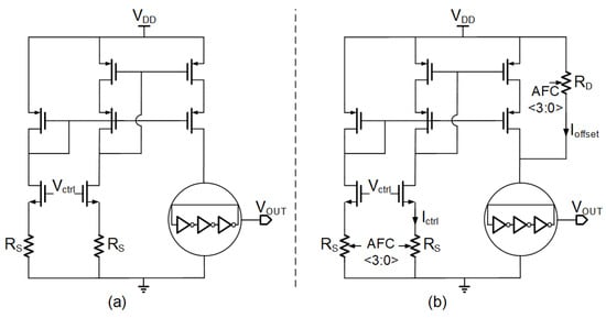
Figure 2.
The schematic of (a) the conventional Ring-VCO and (b) the proposed Ring-VCO.
In the conventional VCO, the input voltage is converted into through the input transistor and the resistance at its source. controls the output frequency , represented as Equations (4) and (5):
Here, denotes the transconductance of the input transistor. is much larger than , enhancing the linearity of the voltage–current conversion. can be represented as , which is an approximately constant value.
In the proposed VCO, variable resistive matrixes and are introduced. The control current of the ring oscillator is the sum of and . Here, and are represented as follows:
Based on different coarse tuning results of automatic frequency control, denoted as AFC<3:0>, varying values of and are chosen, leading to corresponding changes in and , thus resulting in different and initial frequencies. By choosing suitable adjustable resistances for and , 13 curves are produced with similar and different initial frequencies, allowing for a broader frequency tuning range with reduced .
The simulation results of the proposed VCO are illustrated in Figure 3. In Figure 3a–c, the AFC code of the curves changes from “0000” to “1100” along the direction of the black arrow. The AFC codes for curves of the same color are also the same. When and differ, the variation in with is shown in Figure 3a, and the change in output frequency with is depicted in Figure 3b. In the proposed VCO, is not a constant value but varies with , which affects by adjusting . When an upward adjustment of the frequency tuning range is required, a smaller is selected, resulting in a larger slope of vs. (Figure 3a). At the same time, a smaller is selected. Since the oscillator and are on the same branch, the oscillator divides the voltage more and increases. From Equation (7), the slope of the output frequency vs. becomes smaller (Figure 3b). By choosing the appropriate and , it is possible to make the slope of vs. larger to the same extent as the slope of output frequency vs. is smaller, so that the slope of output frequency vs. is almost constant. In other words, smaller and larger values keep nearly constant.
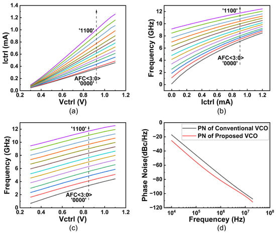
Figure 3.
The simulation results of (a) vs. ; (b) frequency vs. ; (c) frequency tuning curve; and (d) phase noise of the proposed VCO.
As illustrated in Figure 3c, by selecting the resistance values of and appropriately, 13 curves are obtained with close and different initial frequencies. Compared to the conventional VCO with a larger shown in Figure 2a, the simulation demonstrates better noise characteristics, as shown in Figure 3d.
Due to the variable resistance matrixes and reduced , the phase noise of the proposed VCO is significantly decreased. Furthermore, the is consistent across different curves while maintaining high linearity. Only three additional resistor matrixes are required in this method, which enables minimal increase in area and power consumption.
The results across the PVTs (processes, voltages, temperatures) of the proposed VCO in post-layout simulation are shown in Table 1. The temperature variation range is from −40 °C to 125 °C, and the supply voltage variation range is from 1.65 V to 1.9 V. The process corners considered include SPSN, FPFN, SPFN, FPSN, and TPTN.

Table 1.
The results across PVTs of the proposed VCO in post-layout simulation.
The PVT results show that the frequency tuning range exhibits minor variations with changes in temperature, supply voltage, and process corners. Moreover, in each corner, by selecting different tuning curves, a wide frequency range from low frequencies up to over 10 GHz can be covered. The variation rate of is maintained below 23.8% in all cases, achieving extremely high tuning linearity. The phase noise shows small variations, indicating that the proposed VCO can maintain similar phase noise performance across different corners. The power consumption has slightly larger variations but is still within an acceptable range. These results reflect the high stability of the proposed VCO under different temperatures, supply voltages, and process corners, showcasing its robustness and reliability in various operating conditions.
3. The Structure of the Proposed PLL
The block diagram of the proposed PLL is depicted in Figure 4. It comprises various components including a phase frequency detector (PFD), a charge pump (CP), a low-pass filter (LPF), a Ring-VCO, a divide-by-two circuit (DIV2), a multi-modulus divider (MMD), a delta-sigma modulator (DSM) with automatic frequency control (AFC), and a post divider.
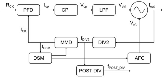
Figure 4.
Circuit block diagram of the proposed PLL.
The PFD compares the phase and frequency of the reference clock signal and the feedback clock signal . The result of this comparison is sent to the CP as a current . CP then converts into a voltage , which is subsequently filtered by the LPF. The output voltage of the LPF regulates the frequency of the Ring-VCO. The output frequency of the Ring-VCO serves as the output of the PLL. It is divided by a high-speed divider-by-two and then further divided by an MMD that can divide by 16 to 255, allowing for capture of different feedback signals. The fractional division function is achieved by using a DSM, which includes AFC. Before PLL lock-in, the frequency is adjusted by utilizing the AFC, which selects a frequency curve that includes the desired target frequency by sending a four-bit code to the VCO. A post divider is employed to divide the high-frequency signal by 16, 32, or 64 to facilitate testing purposes.
The noise from each aforementioned component can be represented by different types of noise signals injected at various nodes in the loop. These injected noises propagate through different feedforward and feedback paths to the output, resulting in corresponding phase noise components.
The simulation results of the overall noise of the PLL in integer-N mode are demonstrated in Figure 5. The results are obtained by post-layout simulation of phase noise for each module and then synthesized through MATLAB R2021a. The overall phase noise of the proposed PLL shown in Figure 5b is lower than that of the conventional PLL shown in Figure 5a. At low frequencies, the phase noise of the VCO is reduced, making the total phase noise lower. At high frequencies, since the noise transmission of the LPF is positively correlated with , the noise reduction in the LPF at high frequencies makes the total phase noise lower.
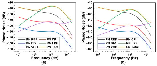
Figure 5.
Overall phase noise simulation results of (a) the conventional PLL and (b) the proposed PLL.
4. Test Results and Discussions
The proposed fractional-N PLL with a small area and low power consumption was implemented using 12 nm FinFET technology. Figure 6 shows a micrograph of the chip, with the PLL occupying an area of 0.078 mm2. The PLL layout is shown in the right part of the figure. The LPF, which utilizes a large number of capacitors and resistors, occupies the largest area. Considering the requirements for bandwidth and stability, it is difficult to reduce its area. The oscillator in the VCO only occupies a small area, protected by guard rings to enhance its stability.
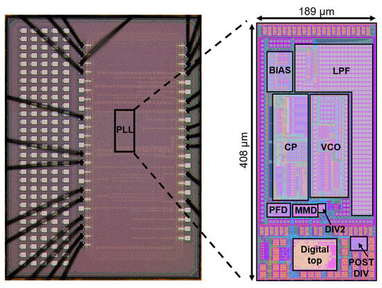
Figure 6.
Die micrograph of the PLL.
The waveform was observed and captured by an oscilloscope (Tektronix MSO64B, Beaverton, OR, USA) and the spectrum and phase noise were measured by a spectrometer (Keysight 9030B, Santa Clara, CA, USA). Figure 7a displays the output of the VCO measured at the divide-by-two output, while Figure 7b shows the spectrum after dividing this output by 16. When the reference clock is 80 MHz and the PLL is divided by 16, the VCO output frequency should be 1.28 GHz. At this time, the output frequency of DIV2 is 640.6 MHz and the output swing is 2.153 V, which is marked in the red rectangle of Figure 7a. In order to measure the phase noise and jitter performance more accurately, the results of DIV2 were tested in the spectrometer after 16 divisions, and its peak was located at 40.04 MHz, which is demonstrated in the red rectangle in Figure 7b. These results show that the proposed PLL can work properly.
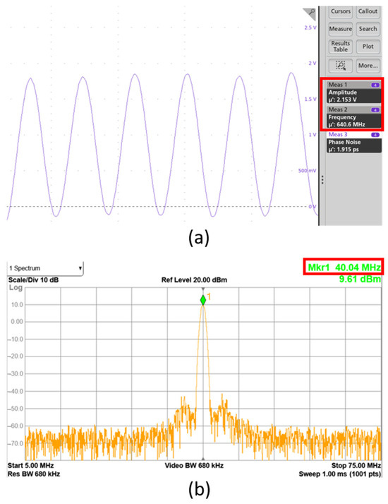
Figure 7.
The (a) waveform and (b) spectrum of VCO output.
The main target applications of the proposed PLL are mobile RF transceivers for 2.4 GHz/5 GHz wireless communications. The 2.4 GHz band has a small range of 2.4–2.4835 GHz, and 14 sub-channels in a bandwidth of only 83.5 MHz, which requires more accurate fractional frequency division. The 5 GHz band has a larger range of 5.15–5.855 GHz, so integer frequency division can meet the demand. Therefore, we tested the performance of integer-N mode at 5.76 GHz and the performance of fractional-N mode at 3.19 GHz to conform to the respective applications. The test frequency of fractional-N mode was slightly larger than 2.4 GHz to demonstrate that it not only covers the 2.4 GHz application but also adapts to other potential applications.
The RMS jitter was tested using a reference input clock of 60 MHz. And the output signal of PLL is tested after dividing the frequency, which shows no impact on the size of the RMS jitter. In integer-N mode, the feedback frequency of the PLL is equal to the 60 MHz input frequency by dividing the frequency by 96 in the PLL. Therefore, the output frequency of the PLL is 60 MHz × 96 = 5.76 GHz. This frequency was tested after 32 divisions, so the integer division test frequency is 180 MHz. In the test of fractional-N mode, the division ratio is 53.25. Here, the output frequency of the PLL is 60 MHz × 53.25 = 3.195 GHz. This frequency was tested after 32 divisions and therefore the integer divided frequency was tested at 99.84375 MHz.
The phase noise performance of the PLL output in integer-N mode is shown in Figure 8. The orange curve represents the measured values, while the green curve represents the fitted values. The start and stop frequencies for the test are marked in the lower red rectangle of Figure 8, and the carrier frequency and RMS jitter are marked in the upper red rectangle. The actual output frequency of the PLL is 5.76 GHz, and the tested frequency is 180 MHz after 32 divisions. The RMS jitter integrated from 0.1 kHz to 10 MHz is 2.702 ps. The measured phase noise is −113.11 dBc/Hz at 1 MHz offset frequency.
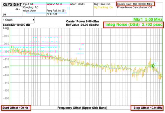
Figure 8.
Measured phase noise of the proposed PLL in integer-N mode at a carrier of 180 MHz.
Figure 9 shows the phase noise performance of the PLL output in fractional-N mode. The orange curve is composed of the actual measured values, which are then fitted to obtain the green curve. The start and stop frequencies, carrier frequency, and RMS jitter are likewise marked in the red rectangle. The actual output frequency of the PLL is 3.19 GHz and the test frequency is 99.84 MHz after 32 divisions. The RMS jitter integrated from 0.1 kHz to 10 MHz is 5.068 ps and the measured phase noise is −123.09 dBc/Hz at 1 MHz offset frequency.
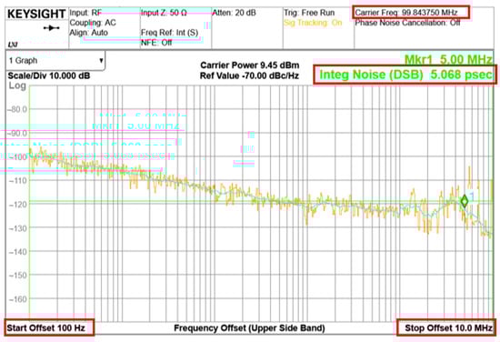
Figure 9.
Measured phase noise of the proposed PLL in fractional-N mode at a carrier of 99.84 MHz.
The RMS jitter and power consumption in integer-N mode across the complete output frequency range are plotted in Figure 10. Within the operational range, the RMS jitter is consistently maintained below 4.5 ps, while power consumption remains below 7.5 mW. Performance comparison between the proposed PLL and other PLLs in recently reported work is summarized in Table 2. The proposed PLL demonstrates advantages in power consumption and area while maintaining low RMS jitter and high output frequency.
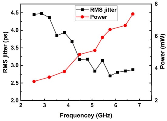
Figure 10.
The RMS jitter and consumption in integer-N mode of the proposed PLL over the frequency range.
Table 2.
Performance summary and comparison with analog PLL.
5. Conclusions
This work presents a compact, low-power, and low-jitter fractional-N PLL using single-ended Ring-VCO with novel resistive matrixes. A novel frequency control method in VCO with high-linearity is proposed, and the great application potential of single-ended Ring-VCOs in FinFETs is demonstrated. Implemented in a 12 nm FinFET process, the proposed PLL occupies only 0.078 mm2. It achieves a 2.702 ps RMS jitter at 5.76 GHz, integrated from 0.1 kHz to 10 MHz, at a power consumption of 6.4 mW. Additionally, it maintains a power consumption below 7.5 mW and an RMS jitter below 4.5 ps over the entire output frequency range of 2.24–6.72 GHz. It can be further applied in mobile applications such as RF transceivers.
Author Contributions
Conceptualization, Y.L.; writing—original draft, Y.L; software, B.X.; validation, Y.S.; methodology, X.X.; data curation, M.L.; writing—review and editing, H.Z.; supervision, Q.S. All authors have read and agreed to the published version of the manuscript.
Funding
This work was supported by the Support Plans for the Youth Top-Notch Talents of China and the National Natural Science Foundation of China (62374036).
Data Availability Statement
The data presented in this study are available on request from the corresponding author.
Conflicts of Interest
The authors declare no conflicts of interest.
References
- Herzel, F.; Razavi, B. A study of oscillator jitter due to supply and substrate noise. IEEE Trans. Circuits Syst. II Analog. Digit. Signal Process. 1999, 46, 56–62. [Google Scholar] [CrossRef]
- Han, Y.; Luo, M.; Zhao, X.; Guerrero, J.M.; Xu, L. Comparative performance evaluation of orthogonal-signal-generators-based single-phase PLL algorithms—A survey. IEEE Trans. Power Electron. 2015, 31, 3932–3944. [Google Scholar] [CrossRef]
- Fahim, A.M.; Elmasry, M.I. A fast lock digital phase-locked-loop architecture for wireless applications. IEEE Trans. Circuits Syst. II Analog. Digit. Signal Process. 2003, 50, 63–72. [Google Scholar] [CrossRef]
- Liu, A.; Huang, Z.; Li, M.; Wan, Y.; Li, W.; Han, T.X.; Liu, C.; Du, R.; Tan, D.K.P.; Lu, J. A survey on fundamental limits of integrated sensing and communication. IEEE Commun. Surv. Tutor. 2022, 24, 994–1034. [Google Scholar] [CrossRef]
- Chillara, V.K.; Liu, Y.-H.; Wang, B.; Ba, A.; Vidojkovic, M.; Philips, K.; de Groot, H.; Staszewski, R.B. 9.8 An 860 μW 2.1-to-2.7 GHz all-digital PLL-based frequency modulator with a DTC-assisted snapshot TDC for WPAN (Bluetooth Smart and ZigBee) applications. In Proceedings of the 2014 IEEE International Solid-State Circuits Conference Digest of Technical Papers (ISSCC), San Francisco, CA, USA, 9–13 February 2014; pp. 172–173. [Google Scholar]
- Staszewski, R.B.; Wallberg, J.L.; Rezeq, S.; Hung, C.-M.; Eliezer, O.E.; Vemulapalli, S.K.; Fernando, C.; Maggio, K.; Staszewski, R.; Barton, N. All-digital PLL and transmitter for mobile phones. IEEE J. Solid-State Circuits 2005, 40, 2469–2482. [Google Scholar] [CrossRef]
- Thamsirianunt, M.; Kwasniewski, T.A. CMOS VCO’s for PLL frequency synthesis in GHz digital mobile radio communications. IEEE J. Solid-State Circuits 1997, 32, 1511–1524. [Google Scholar] [CrossRef]
- Elkholy, A.; Saxena, S.; Nandwana, R.K.; Elshazly, A.; Hanumolu, P.K. A 2.0–5.5 GHz wide bandwidth ring-based digital fractional-N PLL with extended range multi-modulus divider. IEEE J. Solid-State Circuits 2016, 51, 1771–1784. [Google Scholar] [CrossRef]
- Venerus, C.; Galton, I. A TDC-free mostly-digital FDC-PLL frequency synthesizer with a 2.8–3.5 GHz DCO. IEEE J. Solid-State Circuits 2014, 50, 450–463. [Google Scholar] [CrossRef]
- Kwon, K.; Abdelatty, O.A.; Wentzloff, D.D. PLL fractional spur’s impact on FSK spectrum and a synthesizable ADPLL for a Bluetooth transmitter. IEEE J. Solid-State Circuits 2023, 58, 1271–1284. [Google Scholar] [CrossRef]
- Deng, W.; Yang, D.; Ueno, T.; Siriburanon, T.; Kondo, S.; Okada, K.; Matsuzawa, A. A fully synthesizable all-digital PLL with interpolative phase coupled oscillator, current-output DAC, and fine-resolution digital varactor using gated edge injection technique. IEEE J. Solid-State Circuits 2014, 50, 68–80. [Google Scholar] [CrossRef]
- Liu, B.; Zhang, Y.; Qiu, J.; Huang, H.; Sun, Z.; Xu, D.; Zhang, H.; Wang, Y.; Pang, J.; Li, Z. A fully-synthesizable fractional-N injection-locked PLL for digital clocking with triangle/sawtooth spread-spectrum modulation capability in 5-nm CMOS. IEEE Solid-State Circuits Lett. 2020, 3, 34–37. [Google Scholar] [CrossRef]
- Musa, A.; Deng, W.; Siriburanon, T.; Miyahara, M.; Okada, K.; Matsuzawa, A. A compact, low-power and low-jitter dual-loop injection locked PLL using all-digital PVT calibration. IEEE J. Solid-State Circuits 2013, 49, 50–60. [Google Scholar] [CrossRef]
- Wu, W.; Yao, C.-W.; Guo, C.; Chiang, P.-Y.; Chen, L.; Lau, P.-K.; Bai, Z.; Son, S.W.; Cho, T.B. A 14-nm ultra-low jitter fractional-N PLL using a DTC range reduction technique and a reconfigurable dual-core VCO. IEEE J. Solid-State Circuits 2021, 56, 3756–3767. [Google Scholar] [CrossRef]
- Basaligheh, A.; Saffari, P.; Filanovsky, I.M.; Moez, K. A 65–81 GHz CMOS dual-mode VCO using high quality factor transformer-based inductors. IEEE Trans. Circuits Syst. I Regul. Pap. 2020, 67, 4533–4543. [Google Scholar] [CrossRef]
- Kashani, M.H.; Molavi, R.; Mirabbasi, S. A 2.3-mW 26.3-GHz G(m)-boosted differential colpitts VCO with 20% tuning range in 65-nm CMOS. IEEE Trans. Microw. Theory Tech. 2019, 67, 1556–1565. [Google Scholar] [CrossRef]
- Jo, Y.; Kim, J.; Shin, Y.; Hwang, C.; Park, H.; Choi, J. A 135fs rms-jitter 0.6-to-7.7 GHz LO generator using a single LC-VCO-based subsampling PLL and a ring-oscillator-based sub-integer-N frequency multiplier. In Proceedings of the 2023 IEEE International Solid-State Circuits Conference (ISSCC), San Francisco, CA, USA, 19 February 2023; pp. 1–3. [Google Scholar]
- Ye, S.; Jansson, L.; Galton, I. A multiple-crystal interface PLL with VCO realignment to reduce phase noise. IEEE J. Solid-State Circuits 2002, 37, 1795–1803. [Google Scholar]
- Park, P.; Park, D.; Cho, S. A 2.4 GHz fractional-N frequency synthesizer with high-OSR ΔΣ modulator and nested PLL. IEEE J. Solid-State Circuits 2012, 47, 2433–2443. [Google Scholar] [CrossRef]
- Lee, Y.; Seong, T.; Yoo, S.; Choi, J. A low-jitter and low-reference-spur ring-VCO-based switched-loop filter PLL using a fast phase-error correction technique. IEEE J. Solid-State Circuits 2017, 53, 1192–1202. [Google Scholar] [CrossRef]
- Huang, Z.; Jiang, B.; Li, L.; Luong, H.C. 2.3 A 4.2 µs-settling-time 3rd-order 2.1 GHz phase-noise-rejection PLL using a cascaded time-amplified clock-skew sub-sampling DLL. In Proceedings of the 2016 IEEE International Solid-State Circuits Conference (ISSCC), San Francisco, CA, USA, 31 January–4 February 2016; pp. 40–41. [Google Scholar]
- Choi, S.; Yoo, S.; Choi, J. 10.7 A 185fsrms-integrated-jitter and −245dB FOM PVT-robust ring-VCO-based injection-locked clock multiplier with a continuous frequency-tracking loop using a replica-delay cell and a dual-edge phase detector. In Proceedings of the 2016 IEEE International Solid-State Circuits Conference (ISSCC), San Francisco, CA, USA, 31 January–4 February 2016; pp. 194–195. [Google Scholar]
- Yang, S.; Yin, J.; Mak, P.-I.; Martins, R.P. A 0.0056-mm2 −249-dB-FoM all-digital MDLL using a block-sharing offset-free frequency-tracking loop and dual multiplexed-ring VCOs. IEEE J. Solid-State Circuits 2018, 54, 88–98. [Google Scholar] [CrossRef]
- Saxena, S.; Srikanth, M.; Jawale, S.; Sakthivel, R. Efficient VCO using FinFET. Indian J. Sci. Technol. 2015, 8, 262–270. [Google Scholar] [CrossRef]
- Kim, S.; Ham, B.; Cho, M.; Oh, S.; Lee, J.; Cho, T.B. A 14 nm FinFET Sub-Picosecond Jitter Fractional-N Ring PLL for 5G Wireless Communication. In Proceedings of the 2018 IEEE Radio Frequency Integrated Circuits Symposium (RFIC), Philadelphia, PA, USA, 10–12 June 2018; pp. 40–43. [Google Scholar]
- Zou, W.; Ren, D.; Zou, X. A wideband low-jitter PLL with an optimized Ring-VCO. IEICE Electron. Express 2020, 17, 20190703. [Google Scholar] [CrossRef]
- Kundu, S.; Kim, B.; Kim, C.H. 19.2 A 0.2-to-1.45 GHz subsampling fractional-N all-digital MDLL with zero-offset aperture PD-based spur cancellation and in-situ timing mismatch detection. In Proceedings of the 2016 IEEE International Solid-State Circuits Conference (ISSCC), San Francisco, CA, USA, 31 January–4 February 2016; pp. 326–327. [Google Scholar]
- Wang, B.; Yang, H.; Jia, Y. A 1-to-3 GHz 5-to-512 multiplier adaptive fast-locking self-biased PLL in 28 nm CMOS. Electronics 2022, 11, 1954. [Google Scholar] [CrossRef]
- Wang, J.S.; Chou, P.Y. Clock Period-Jitter Measurement with Low-Noise Runtime Calibration for Chips in FinFET CMOS. IEEE Trans. Circuits Syst. I Regul. Pap. 2024, 71, 3157–3164. [Google Scholar] [CrossRef]


Disclaimer/Publisher’s Note: The statements, opinions and data contained in all publications are solely those of the individual author(s) and contributor(s) and not of MDPI and/or the editor(s). MDPI and/or the editor(s) disclaim responsibility for any injury to people or property resulting from any ideas, methods, instructions or products referred to in the content. |
© 2024 by the authors. Licensee MDPI, Basel, Switzerland. This article is an open access article distributed under the terms and conditions of the Creative Commons Attribution (CC BY) license (https://creativecommons.org/licenses/by/4.0/).