Article

An Experimental Investigation of Noise Sources’ Contribution in the Multi-Chip Module Open-Loop Comb-Drive Capacitive MEMS Accelerometer

Department of Microelectronics and Computer Science, Lodz University of Technology, 93-005 Lodz, Poland
*
Author to whom correspondence should be addressed.
Electronics 2024, 13(13), 2599; https://doi.org/10.3390/electronics13132599
Submission received: 9 May 2024 / Revised: 25 June 2024 / Accepted: 27 June 2024 / Published: 2 July 2024
(This article belongs to the Section Microelectronics)

Abstract

:
The paper presents the noise analysis of a MEMS and ASIC readout integrated circuit (ROIC) constituting the accelerometer developed in the frame of the InnoReh project, aiming at the development of methods for monitoring patients with imbalance disorders. Several experiments were performed at different temperatures and in different configurations: ROIC alone, ROIC with emulated parasitic capacitances, MEMS and ROIC in separate packages, and MEMS and ROIC in a single package. Many noise/interference sources were considered. The results obtained experimentally were compared to the results of theoretical investigations and were within the same order of magnitude, although in practice, the observed noise was always greater than the theoretical estimation. The paper also includes an in-depth analysis to explain these differences. Moreover, it is argued that, in terms of noise, the MEMS sensing element, and not the ROIC, is the quality-limiting factor.

1. Introduction

Microelectromechanical system (MEMS) inertial sensors are widely found in many modern applications. Especially, accelerometers and gyroscopes are used in many devices such as smartphones [1,2], drones [3,4], cars [5,6], wearable devices [7,8], etc. [9]. Moreover, because of miniaturization, low cost, low power consumption, and great performance, they are used in medical applications providing remote patient diagnosis without affecting normal functioning. One of the applications is medical devices used for monitoring patients with balance disorders [10,11,12].
In particular, MEMS-based accelerometers may be helpful in medical examinations like posturography [13] to help doctors provide a clinical assessment of the patient’s balance and posture control [11]. Such a system was designed in the frame of the Innovative Rehabilitation (InnoReh) project [13], which in its default design used off-the-shelf commercial accelerometers. However, a part of the project focused on designing and manufacturing an alternative, custom 3D axis accelerometer for this purpose. The detailed description of the designed accelerometer is presented in [14]. In short, it is composed of two main parts:
  • A 3D capacitive comb-drive acceleration sensor manufactured using dedicated MEMS technology, XMB10 by XFAB [15];
  • An electronic readout circuit, based on a switching-capacitor architecture, manufactured using a relatively standard XP018 CMOS mixed-signal technology by XFAB [16].
Both parts were then integrated into one package using wire bonding and tested. The measurements performed proved that both the MEMS sensor and the readout integrated circuit (ROIC) work correctly, and proper acceleration readouts can be achieved using the designed accelerometer, i.e., the obtained parameters were satisfactory. However, although the device met the project requirements, the measured level of noise was surprisingly high. Therefore, during the course of the project, dedicated research was aimed at identifying the sources of noise that could have produced such noise levels. In this paper, we performed an in-depth analysis of all sources of noise in the designed 3D accelerometer, both in the MEMS sensor part and the ROIC part. Comparing the results from various measurements and many different test setups allowed determining the impact of every noise source on the total value of the noise. One of the most important contributions of this paper is precisely quantifying the exact value of the noise produced separately by the EMS sensor part and the ROIC part. This was possible thanks to the fact that, in addition to the default accelerometer structure (in which both parts were integrated in a single package), during the project, the MEMS sensor and ROIC were also manufactured in completely separate packages, whose noise levels were subsequently measured. Thus, it was possible to practically determine how much of the total output accelerometer noise came from the capacitive sensor itself and how much was produced by electronic readout circuit.

1.1. MEMS Sensor Design

The basic investigation of noise and temperature dependence can be performed in the modeling phase [17,18]. The desired sensor performance is achieved through the proper definition of the sensor shape and dimensions. Moreover, this also determines the sensor noise performance. Our X-axis accelerometer is presented in Figure 1 [14]. It uses a comb-drive structure fabricated with X-FAB XMB10 technology. This technology allows fabricating single-, double-, or triple-axis inertial sensors such as accelerometers and gyroscopes. It uses cavity Silicon On Insulator (SOI) wafer-based technology, deep reactive-ion etching (DRIE) for the sensor elements’ creation, and top cap wafer with etched cavities and bond pad openings [19,20]. Three wafers were used in the fabrication. At the bottom, there is a cavity wafer. It is directly bonded to the membrane SOI wafer, which comprises the main structure of the accelerometer. Finally, the sensor is encapsulated with the top cap wafer bonded with the glass frit wafer. Our goal was to design an accelerometer with high sensitivity and high initial capacitance in order to simplify the readout circuit. Due to the low response frequency (dozens of Hz), the size of the accelerometer could be relatively large. The total size of the accelerometer is 1.3 mm × 0.93 mm and is dependent on the maximal finger length allowed in the technology used. Due to this fact, the proof mass is an H-shaped structure, which allows increasing the number of fingers. The proof mass is suspended over the frame with a suspension that can be described by a simple Newton’s law of motion equation [9].
The suspension in our sensor consists of eight springs (parallel connection). Each spring is made of two beams connected in series (folded beam) to decrease suspension stiffness. The total stiffness coefficient can be calculated using the following formula using the relation for the fixed-guided beam [21]:
k = 8 2 k b e a m , k b e a m = 12 E I l 3 , I = b h 3 12
where k b e a m is the stiffness of a single fixed-guided beam, E is Young’s modulus, I is the moment of inertia, and l , b , and h are the single beam length, width, and thickness, respectively. All parameters of the designed accelerometer are listed in Table 1.

1.2. Readout Integrated Circuit (ROIC) Design

The overall concept of the application of the MEMS and ROIC structures in the so-called MEDIPOST device (Figure 2a) along with the basic idea of the device’s operation (Figure 2b) is presented and discussed in [11,14]. The designed and manufactured MEMS comprises three capacitive accelerometers for the X, Y, and Z axes. The principles and design are introduced in [14] and thoroughly discussed in [22]. The readout integrated circuit (ROIC) provides a separate analog readout channel with separate ADCs for each axis of the MEMS accelerometer. The readout signals are converted from the analog to digital domain and collected by the processing and serial communication interface (Figure 2a). The ROIC was designed according to the requirements of the InnoReh project with the usage of XP018 0.18 micron CMOS analog mixed-signal process technology. The ROIC structure is introduced and discussed in [23].
Figure 3 presents the block diagram of a single readout channel of the ROIC. MCC means the Mismatch Capacitance Compensation system, and DCC is the aforementioned Digital Control Circuit. The operation of the analog channels of the ROIC is based on the discrete-time switched-capacitor principle. MEMS capacitors are connected to analog ROIC inputs, and samples of the charge collected by these capacitors are converted to voltages. These voltages are processed with cascaded differential OPAMPs (C2V and AMP1) and provided to the final AMP2 OPAMP. This OPAMP serves as a differential to single-ended converter and is equipped with programmable gain functionality. The output voltage of this OPAMP is provided to the internal ADC and converted with 10-bit resolution.
The differential amplifiers used in the analog signal path [24] are based on amplifiers designed especially for switched-capacitor applications [25]. Such OPAMPs are well suited for operation with low [26] and very low supply voltages [27,28]. Low-voltage operation is not an issue in the case of the ROIC discussed in this paper. However, the adopted OPAMP structure introduces additional internal circuitry for gain enhancements [29]. Interestingly, this modification provides very good control over crosscurrents in the OPAMP output stages over a wide range of supply voltage values. Thus, the overall complexity of the differential OPAMPs is low.

1.3. Noise in Capacitive MEMS Accelerometers

The main sources of noise in capacitive MEMS accelerometers are the following:
  • Brownian noise due to random movement of the proof mass, including squeeze-film damping effects;
  • Thermal noise of the switches present in the switching-capacitor circuit;
  • Thermal and flicker noise of the capacitance-to-voltage converter;
  • Noise of the reference voltage, which is used to periodically charge MEMS capacitors.
The theoretical value of the Brownian noise is given by Equation (2) [30].
a n o i s e = 4 k B T ω 0 m Q = 8 k B T π f 0 m Q
where Q is the quality factor, T is the temperature, m is the device mass, k B is the Boltzmann constant, and f 0 is the first resonant frequency. Substituting the parameters of the designed accelerometer from Table 1 into Equation (2), we obtain the total Brownian noise to be a n o i s e = 3.1 μ g/ H z at room temperature, where g denotes gravitational acceleration.
The thermal noise of the switches in the ROIC can be calculated with Equation (3) [31]
e n , s w i t c h = 4 k B T C i n t f s
where C i n t is the integration capacitance in the feedback loop of the capacitance-to-voltage (C2V) converter and f s is the sampling frequency. The calculated value of this type of noise for the designed ROIC is equal to 0.26 μ V/ H z .
Perhaps the most important noise source in the ROIC is the noise of the amplifier in the C2V circuit, given by Equation (4) [32]. Since the correlated double-sampling technique was implemented, the thermal noise is dominant here and flicker noise (1/f noise) can be safely neglected.
e n , a m p = 16 3 C s + C p + C i n t + C d s C i n t 4 k B T C o u t f s
where C s is the sensor capacitance, C p is the sum of parasitic capacitances on the signal lines between the MEMS and ROIC, C o u t is the capacitance at the C2V output, and C d s is the value of the capacitors used for correlated double-sampling. The exact values of parasitic capacitance C p are usually difficult to estimate. However, using a Summit 11,000 probe station by Cascade Microtech [33] and an E4990A impedance analyzer by Keysight Technologies [34], it was possible to measure C p = 18 pF, which results in the value of the noise being 1.47 μ V/ H z .
Finally, the charging reference noise can be calculated using Equation (5) [31].
e n , r e f = 2 e n 2 C s C i n t 2 f s R s w
where e n is the noise of the reference voltage source and R s w is the resistance of the switches. Taking the theoretical value of V n given by the manufacturer from the technological library used, the approximate value of this type of noise for the designed ROIC amounts to 0.1 μ V/ H z .

1.4. Motivation

Even if all above-mentioned noise sources are added up, the resulting total calculated noise is not very high. Nevertheless, when measurements were performed, the measured output noise was discovered to be an order of magnitude higher than the calculated noise. In particular, the measured noise values were 10-times higher in the case of the MEMS and ROIC setup and about 6-times higher for the ROIC-only setup. Such a discrepancy is not unusual, as other researchers have also reported the measured accelerometer noise to be much higher than the accelerometer noise calculated theoretically, even several times higher in some cases [35,36,37,38]. However, most authors do not analyze these differences in depth, attributing them to inaccurate noise calculation models or environmental interferences during the measurements.
Therefore, such a discrepancy between the calculated and measured noise levels in our designed accelerometer was a motivation for an in-depth analysis of the noise sources in the designed accelerometer. It is worth emphasizing that our accelerometer design is particularly suited for such an analysis because of the following reasons:
  • The MEMS and ROIC were manufactured in different package versions, both as separate chips and as one bonded package, which allows quantifying the noise introduced by the MEMS and ROIC separately, as well as analyzing the impact of the package and PCB on noise.
  • The ROIC is easily configurable, for example the gain, modulation voltage, and switching frequency can all be freely configured and their impact on noise can, therefore, be analyzed.
  • Dedicated test points on the ROIC layout allow measuring the signals from inside of the ROIC itself and, thus, finding the noise levels after each stage of the ROIC.
  • The wireless acquisition of samples allows easy measurements inside a thermal chamber, which allow, in turn, very precise measurements of the dependence of the noise on the temperature.
Table 2 shows the breakdown of the noise from each source calculated in μ g/ H z . Two cases are considered in the two leftmost columns: first, when both the MEMS and ROIC operate together; second, which is the ROIC-only setup. As can be seen, the amplifier noise is the dominant source of calculated noise in both cases. It is considerably higher in the case of the MEMS and ROIC setup due to the relatively large parasitic capacitances introduced by the MEMS sensor. Therefore, one more case was added to our analysis: the third column includes the corresponding calculations and measurements for the case in which the ROIC-only setup is connected to dummy capacitors, which imitate the MEMS and parasitic capacitors. The results show that, even with artificially added parasitic capacitors, the noise is still much lower than that obtained for the MEMS and ROIC setup. This poses a quite interesting question: where does this high measured noise level come from?
In the following sections, we present the detailed description of the performed measurements, which aim at finding the reason for such a discrepancy between the calculated and measured noise, as well as experimentally identifying and quantifying the contribution of various noise sources to the total noise in the analyzed accelerometer.

2. Materials and Methods

2.1. Devices under Test and Their Setups

2.1.1. General Test Setup Information

The base of the utilized test setups is the above-mentioned ROIC and MEMS structures. They are briefly introduced in Section 1.1 and Section 1.2, while the details and aspects of their structure and operation are discussed in [14,22,23,24,39]. Full layouts of the MEMS and ROIC designs, as well as microphotos of the manufactured structures are presented in Figure 4. The considerations presented in this article are based on the measurements and analysis of the accelerometer and readout circuit for the X axis.
The number of setups for which the measurement results are presented in this article is motivated by the necessity to gather representative information on the performance of ROICs alone and in cooperation with MEMS structures. Such an approach is expected to make it possible to discern general relationships and to distinguish them from the scatter of properties between different ROIC, MEMS, and PCB specimens.
During the works related to the InnoReh project, several ROIC-only and MEMS and ROIC chips, i.e., devices under test (DUTs), installed in their test setups were scrutinized. They are introduced in Table 3, where their naming convention and structure are introduced. It can be observed that the names of the test setups were mainly derived from the ROIC and MEMS specimens, which were used and tested in them.
All introduced test setups used several variants of the test PCBs housing all necessary electronics and DUTs. Apart from the ROIC or MEMS and ROIC DUTs, these PCBs are equipped with supply modules and wireless communication devices that communicate with the digital part of the ROIC in order to program it and receive data from the analog readout blocks. The test setups communicate via a WiFi network and can be remotely operated. The operation quality of several test setups (including noise properties and thermal dependencies) was already analyzed with a wide range of measurements [24,39]. All presented test setup variants enable proper and reliable measurement results, which are presented and discussed in this paper.

2.1.2. ROIC DUTs and Test Setups

The ROIC-only setups are focused on testing the ROIC specimens only, with no MEMS at their analog inputs. Tests were performed for six ROIC-only test setups based on different variants of the test PCBs, as explained in the test and summarized in Table 3. Figure 5 presents all the ROIC setup types used during the measurements discussed in the paper. The ROIC #1 test setup is based on the first version of the test PCB with the ROIC #1 chip specimen and presented in Figure 5a. The ROIC specimens #2, #3, #4, and #6 were soldered to specimens of version no. 2 of the test PCB. One of such PCBs is shown in Figure 5b. Figure 5c presents the test setup used for the ROIC #4 specimen before and after disconnecting its analog inputs from the package pins (that is why the chip lid is removed). Figure 5d presents the ROIC #6 test setup used for measurements without and with ceramic capacitors instead of the MEMS chip. Interestingly, Figure 6c shows the test PCB with the QFN-100 socket and reused by the ROIC #5 test setup. This setup is in fact a reuse of the modified MEMS and ROIC #3 setup, explained later in this and the following text subsections and included in Table 3.
Two of the presented test setup types are based on test PCBs intended for use with MEMS and ROIC specimens placed in two separate QFN-100 packages (the 2× QFN packages mentioned in Table 3) and shown in Figure 5a,b,d. Because the ROIC analog input is equipped with the capacitive trimming circuitry, it is possible for the ROICs to operate without the MEMS at its analog inputs [23]. It was found that the ROIC specimens can operate soldered to the utilized PCBs and using trimming circuitry to equalize the total capacitances present at the ROIC analog inputs.
Version #1 and #2 of the PCBs were redesigned to a limited extent and manufactured by different providers. ROIC #1 was soldered to specimen #1 of test PCB version 1. ROICs #2 and #3 were soldered to the same specimen #1 of test PCB version 2. Thus, the influence of the test PCB is expected to be identical in the case of both of these ROIC test setups. ROIC #4 was soldered to specimen #2 of test PCB version 2. Moreover, ROIC #4 has been tested in two different configurations. First, it was soldered to a test PCB and tested as another ROIC-only test setup. During the tests, it was found that some residue related to the soldering process must have remained, which altered the ROIC operation for temperatures above 70 °C. The PCB was extensively rinsed and measured again. Though discernible improvement in operation quality was observed, the ROIC and its test PCB did not work fully properly. Resoldering the ROIC might have damaged its package made of plastic base and lid glued together. Instead, the decision was made to open the package lid and to remove the interconnections between the analog inputs of the ROIC and the internal pins of the package. The resulting structure and close-up of a few removed connections is presented in Figure 7. All above-mentioned test setups based on ROIC #4 bear its name, but with appropriate annotations.
ROIC #5 is a single ROIC-only test setup based on the test PCB intended for use with the MEMS and ROIC specimen consisting of MEMS and ROIC placed in a single QFN-100 package and interconnected. This test setup uses the universal test PCB equipped with a QFN-100 test socket. The socket itself is presented in Figure 8a. Figure 8b shows it during assembly on its test PCB, while Figure 6c presents the working PCB during tests. The ROIC #5 test setup is in fact the MEMS and ROIC #3 setup with the MEMS-ROIC interconnections removed (Figure 9). The fault in the MEMS and ROIC #3 setup specimen manifested itself with a saturated readout value for channel X, regardless of the applied acceleration. The MEMS–ROIC interconnection removal ended with the fully functional ROIC #5 setup (Figure 5c) with its readout values correctly reacting to the trimmer circuit settings. Thus, the MEMS was found to be the faulty component of the setup, while the new ROIC setup was further tested.
In total, two different ROIC specimens have had their input connections exposed to the outside environment. Moreover, these two ROICs are based on different test setups. ROIC #5 is a MEMS and ROIC setup in a single QFN-100 package, while ROIC#4 is an ROIC-only setup in a QFN-100 package and each of these ROIC samples was tested with a different PCB board. These two setups with disconnected analog inputs of the ROIC specimens provide the possibility of testing the influence of the external environment (i.e., powered test PCB) on the operation on the ROICs.

2.1.3. MEMS and ROIC DUTs and Test Setups

The measurements discussed in the paper were performed for five MEMS and ROIC test setups based on four different PCB variants (Table 3). Figure 6a presents the first version of the PCB intended to solder the MEMS and ROIC specimens in a single package (1× QFN packages according to Table 3) and used for the MEMS and ROIC #1 test setup. Figure 6b presents the second version of this test PCB used for the MEMS and ROIC #2 test setup. Figure 6c presents the aforementioned PCB endowed with the test socket for MEMS and ROIC structures placed in a single QFN-100 package and used with MEMS and ROIC specimens #3 and #5. The test PCB intended for MEMS and ROIC structures placed in separate packages, also widely used for the ROIC-only setups, was used according to its original purpose as a part of the MEMS, PCB, and ROIC #1 setup, presented in Figure 6d.
The QFN-100 package used by the manufacturer of the MEMS and ROIC dies is intended mainly for prototyping purposes. It has different dimensions such that typical commercial QFN-100 packages and available test sockets need to be modified for use with the non-standard package of the MEMS and ROIC setup. The QFN-100 type package is a complex structure, as it has multiple pads placed every 0.4 mm with a separation of about 0.25 mm. However, there are few manufacturers who provide test sockets for this package type. The two most promising candidates were selected and acquired. These test sockets are presented in Figure 8a. They represent different mechanical approaches, and after the initial test, the clam shell-type socket was found to be suitable for the required modifications. It was possible to remove the lid inlet and replace it with a flatter one. Also, this specific socket type is able to house the non-typically wider package and provide the full set of electrical connections. The MEMS and ROIC setup test PCB for the adapted test socket was designed and manufactured and is presented in Figure 8b with the test socket already soldered. This test board was used with several MEMS and ROIC chips (Table 3, Figure 6c), also in the thermal chamber, as shown in Figure 10.

2.2. Measurement Setup

This article discusses noise phenomena in the integrated structures under scrutiny. The measurements that show the behavior of the tested structures are mainly presented in relation to temperature. This way, the operation of the ROIC and MEMS and ROIC setups is presented as the thermal (or temperature) dependencies of the accordingly scaled mean readout values (based on 5000 samples per readout), as well as the standard deviations of these readouts. The inclusion of temperature dependencies in the presented results is helpful in the process of finding the causes and sources of noise through the elimination of those with different thermal dependencies.
The measured test setups were subjected to static tests. To check the sensitivity of the test setups, various positioning was implemented to make use of Earth’s gravity. The sensitivity tests are discussed in [14]. Several types of tests were conducted at room temperature. However, the most informative and revealing ones were performed with the use of the Binder MKF 115 E4 climate chamber [40]. All thermal tests covered a temperature range of −40 °C to 100 °C. The measurement setups used during the test sessions discussed in the paper are introduced in [24,39]. In general, the PCB-based test setup was heated up to 100 °C and then gradually cooled down to −40 °C. Measurements were taken every 1 °C for a selected set of voltage gains available in the analog readout module.
The earlier version of the setup required powering the PCB before each readout series and shutting it down just afterwards, for better cooling of the ROIC or MEMS and ROIC components of the test setup. The current version of the thermal test setup uses the continuously powered PCB test board, with no shutdown episodes at all. The very slow decrease in chamber temperature combined with the low power consumption of the MEMS and ROIC structures ensured proper readout results. Most of the presented measurements were based on this simplified test setup, with no loss of the result quality compared to the original procedure. The complete measurement event at each temperature consisted of 5000 consecutive readouts. Such a sample number enables statistical analyses to cope with potential noise influence and the resulting quality issues of the processed signals.
Apart from measurements, the operation of the ROIC and MEMS and ROIC specimens was checked during the design and later with simulations performed with Cadence Virtuoso IC suite. Because the encountered phenomena found in the MEMS and ROIC setups included unusual noise effects, noise simulations in the time domain were performed in an attempt to inspect the properties of the analog readout block. This approach was possible due to the fact that the MOS transistor models included in the process kit are equipped with noise models and the readout block consists of low-voltage MOS devices with only a limited number of capacitors. The noise models and parameters include both 1/f and thermal noise. These types of noise are important contributors, and their influence on the operation of MOS devices is discussed in [41,42], respectively.
The simulated noise influence was found to be significantly lower than obtained during the measurements [24]. This issue was discussed with the foundry engineers. According to the obtained information, the noise models and parameters used for all low-voltage MOS devices are limited in their capabilities and less advanced than those implemented for high-voltage MOS devices available in the utilized technology process. Nevertheless, the noise simulations still helped to find the main contributors to the output noise of the analog signal path. The main suspects are the differential OPAMPs used in the analog readout path (Figure 3) (in C2V and AMP1 blocks) as they have higher internal complexity compared to the single-ended AMP2 OPAMP at the end of the analog processing path.

3. Results

Unless otherwise noted in the text of this and the following sections, the terms ROIC, MEMS and ROIC (M&R), and MEMS, PCB, and ROIC (M&P&R) only with related numbers refer to the test setups consisting of the ROIC or MEMS and ROIC chips connected to their respective PCBs, along with all auxiliary components and modules (as described in Table 3).

3.1. Full Package (MEMS and ROIC) Measurements

3.1.1. Variability across Specimens

Thermal dependence tests of the mean readout value and standard deviation confirmed that there were significant differences of the mean value dependence for different specimens, while the standard deviation of readouts remained similar over all tested specimens. Figure 11a presents the mean values of the readouts obtained with the four different test setups presented in Figure 6. Figure 11b shows the relevant dependencies of the readout standard deviation. All presented temperature dependencies were scaled in the gravitational acceleration g. The thermal dependence of the readout mean values varied significantly in both the values and trends. Only a few of them were monotonic (specimens: M&R #2, M&R #5, and M&P&R #1) or had a single inflection point (M&R #2, M&R #3, and M&R #5), and the maximum ratio of readout mean value spans for different test setup specimen was about 4.9 (M&R #3 vs. M&R #1).

3.1.2. Variability across Measurement Sessions

Figure 12a,b present the test results of the first MEMS and ROIC specimen soldered to the first version of the test PCB (Figure 6a). The M&R #1 is the name of the complete test setup, and letters A to F denote different test sessions to which this test setup was performed. We conducted these sessions over a period of more than a year, and they were taken with versions of the test procedures explained in Section 2.2 and introduced in [24,39]. The obtained results were consistent in the case of both the readout mean value and standard deviation, which shows the stability of the MEMS and ROIC #1 operation and the adequate quality of the utilized versions of the test procedures.
Figure 13a,b show the sets for the test results of the second MEMS and ROIC specimen atop the redesigned PCB version #2 (Figure 6b), referred to as M&R #2. The data sets were obtained during five test sessions performed over a period of one month. The obtained thermal dependence curves nearly overlap, and the mean readout values were even more consistent than in the case of M&R #1. On the other hand, the observed temperature dependence was approximately 3.5–5-times stronger than in the case of M&R #1.
There are two important outcomes based on the presented results. First, there was good repeatability of the results obtained during numerous test sessions performed over long periods of time for both the readout mean value and standard deviation. Second, though the results for the readout mean values over temperature were different and formed distinct sets for each of the test setups (Figure 11a, Figure 12a and Figure 13a), the curves representing the readout standard deviations were similar in the case of M&R #1 and M&R #2 (Figure 11b, Figure 12b and Figure 13b).

3.1.3. Influence of Analog Path Gain

It is also worth noting that the MEMS and ROIC specimens that offered worse (higher) thermal dependence of the mean readout value did not exhibit worse noise behavior. For example, the MEMS and ROIC #1 specimen showed the lowest temperature dependence of the readout mean value (Figure 14a) and the overall worst noise (readout standard deviation) properties of all tested MEMS and ROIC test setups (Figure 14b). On the other hand, the MEMS and ROIC #3 specimen that showed the highest (worst) dependence of the readout mean value also showed the lowest (best) dependence on noise (readout standard deviation) of all the samples tested, as depicted in Figure 15a,b. These results are presented for every component of the final gain that can be set in the AMP2 single-ended OPAMP. The gain of the AMP2 OPAMP can be selected in the range of 1 to 8. The basal gain equal to 1 was provided by the hardwired capacitors (denoted by Cw). The remaining components of the gain were provided by sets of auxiliary capacitors switched on and off with the CMOS transmission gates controlled with a 3-bit gain control word and placed at the input of the AMP2 OPAMP. The capacitances of the capacitors were controlled with bits 0–2 (B0, B1, and B2) of this control word and were equal 1-, 2-, and 4-times the value of the hardwired capacitors, respectively. Thus, these capacitor sets provided gains equal to 1, 2, and 4. Figure 14 and Figure 15 presented the mean value and standard deviation for the Cw, B0, B1/2, and B2/4 components of the AMP2 output, because this way, the influence of all the gain components was normalized to the unity gain.
It was observed that thermal dependencies for each discussed (and all other tested) MEMS and ROIC test setups were not dependent on the gain of the analog readout path of the ROIC. The results obtained were very consistent with the only exception of the standard deviation dependence for the specimens MEMS and ROIC #1 working with a unity gain provided just by the hardwired capacitors around the OPAMP in the AMP2 stage. This phenomenon was encountered only once and never reproduced in any other test setup of any kind nor any type of conducted simulation. This effect is related to the AMP2 signal processing block, and our suspicion points to some local manufacturing defect. This effect was not found in the readout circuits for the Y and Z axes of MEMS and ROIC #1.

3.2. ROIC Tests

3.2.1. Variability across Specimens

Figure 16 presents the thermal dependencies for all tested ROIC specimens and test setups. It can be observed that the thermal dependence of the mean value readout (Figure 16a) is mainly negative, but a positive one is also present. The results differed for various ROIC test setup specimens. The mean readout values also differed in the case of ROICs #2 and #3, soldered to the same PCB (one at a time, of course). On the other hand, the mean readout values for ROIC #3 and disconnected ROIC #4 were very similar. In general, the thermal dependence of the mean readout value for different ROIC specimens showed discernible variability.
On the other hand, the standard deviation dependencies (Figure 16b) were all very similar in shape with a maximum value spread of about 15% between samples. The results for ROIC specimens #2 and #3 (sharing the same PCB) differed for the upper temperature range and were generally more divergent than in the case of ROIC specimens #2 and #4, which were soldered to different PCBs.

3.2.2. Comparison between ROIC-Only and MEMS and ROIC Measurements

The test results for the MEMS and ROIC and ROIC-only test setups provide a substantial amount of information. The thermal dependence of the readout mean value was several times larger in the case of the former test setups. Also, the shapes of the thermal trends for these two types of test setups differed significantly. The MEMS and ROIC test setups showed generally similar trends (Figure 11a) of decreasing values, while in the case of the ROIC test setups, the relevant thermal trends were weaker and more divergent (Figure 16a). As the ROICs constitute a part of any MEMS and ROIC system, it can be stated that the MEMS structures caused the dominant part of the thermal dependence of the readout mean value, and in a way, this eclipsed the ROIC contribution.
The thermal dependence of the readout standard deviation was much more pronounced in the MEMS and ROIC test setups (Figure 11b), but the thermal trends were very similar to those found in the ROIC-only test setups (Figure 16b). The noise levels were found to be about 2.5–2.8-times higher for the ROIC specimens driven with the MEMS structures. However, in both cases, the noise increased by about 15–20% over the entire covered temperature range, that is −40 to 100 °C, and very similar trend shapes were obtained for all tested setups. A General comparison of the measurement conducted for the majority of the MEMS and ROIC and ROIC-only test setups is presented in Figure 17a,b for the mean readouts and standard deviation, respectively.
Of course, different ROIC specimens were tested in different kinds of test setups during the performed measurements. However, there was a case when a MEMS and ROIC chip used for the test with the universal test socket PCB malfunctioned and was reused by disconnecting its analog inputs from its QFN-100 packages. The aforementioned MEMS and ROIC #3 chip was turned into the ROIC #5 specimen. Thus, it was possible to compare the operation of the same ROIC specimen with its analog inputs driven by the MEMS structure, as well as fully disconnected from the influence of the ROIC environment. Figure 18 shows direct comparisons of the operation quality for a single ROIC specimen in these two above-mentioned distinct modes of operation. The thermal dependence of the readout mean value for MEMS and ROIC #3 was different from that of the ROIC #5 specimen in both range and shape. The analogous curves for the readout standard deviation exhibit very similar thermal trends, but the thermal dependence for the former test setup was about 2.7-times larger than for the latter test setup.

3.3. Investigation of Potential Noise Sources

3.3.1. Influence of the PCB

Such different results can be due to numerous reasons. One of them may be the influence of the test PCBs, which may be different for the PCB specimens, versions, and manufacturing processes. The influence of the test PCB cannot be excluded, but the influence of differences can be evaded by the use of one and the same test PCB specimen for all MEMS and ROIC chips. This conclusion triggered the introduction of the universal test PCB for the MEMS and ROIC test setups. This PCB is presented in Figure 6c and Figure 8b. It was used for MEMS and ROIC #3 and #5. The comparison of the temperature dependence obtained for all discussed MEMS and ROIC test setups is presented in Figure 11a (mean readout value) and Figure 11b (readout standard deviation). It can be noted that their standard deviation thermal trends were very similar to the case of the other MEMS and ROIC test setups. The mean value trends for specimens #3 and #5 were clearly distinct and by no means more similar to each other than to the MEMS and ROIC specimens measured with the use of different types of test PCBs. This outcome was also correct for MEMS, PCB, and ROIC #1, based on the MEMS and ROIC in separate packages and connected through their test PCB (Figure 6d).
The influence of the test PCB was also investigated from the ROIC perspective. Figure 19a,b present the thermal dependence of the mean readout value and standard deviation for all sets of ROIC #4 specimen. The original readout curve shows the highest readout value decrease with an increase in temperature and a sharp drop. The same curve after extensive rinsing of the PCB and most probably partial removal of the residue beneath the ROIC enclosure shows less decrease and drop for high temperatures, as presented in Figure 19a. The ASIC after removal of its analog input connections showed the most stable readout values and no drop-off effect. The standard deviation curves show that, whatever amount of residue beneath the package is present, the noise of the ROIC readout path is very similar. It is only the disconnection of the ROIC from the PCB that makes the measured noise smaller. The observed noise level difference is easily observable, but it was rather limited and equal to about 10%.
Moreover, a comparison was made between the ROIC #1 specimen soldered to the PCB and the ROIC #4 and ROIC #5 specimens with their analog inputs disconnected. Figure 20a,b show that both disconnected ROIC specimens had readout standard deviations lower than in the case of the best connected ROIC specimen. However, this observation is not true for the thermal dependence of the readout mean value. ROIC #1 offered the lowest thermal dependence, a few times lower than in the case of any disconnected ROIC specimen.
Thus, it was observed that the influence of the package and the test PCB on the ROIC thermal dependencies (which means DC test conditions) was limited. This was due to the results of the ROIC test setups with disconnected ROIC inputs, and that decision was made to prepare a specimen of the MEMS and ROIC test setup with the MEMS and ROIC structures mounted in separate packages and connected through a test PCB board. Such a test setup (named MEMS, PCB, and ROIC #1 or M&P&R #1) was manufactured and tested. The test setup is presented in Figure 6, and its thermal dependencies are shown in Figure 11. As far as the static tests are concerned, its operation cannot be considered by any means as distinct from those obtained for the other tested setups.

3.3.2. Influence of Input Capacitances

Further research was conducted to investigate the details of the MEMS and ROIC’s cooperation. The MEMS structure designed and utilized in the project comprised two comb capacitors. Specific tests were performed to check whether the substantial increase in noise was caused also by typical, off-the-shelf (non-micromachined) capacitors. Figure 16a,b also show the results for the CAPS and ROIC #1 setup consisting of the previously tested ROIC #6 setup with ceramic capacitors soldered to the analog inputs of ROIC #6. These capacitors have very good thermal stability, while their capacitances were very similar to the values simulated and measured for the MEMS structures (around 3 pF) [14]. The results obtained for this test setup clearly showed readout value and standard deviation dependencies very similar to those of the ROIC-only setups. By the way, this was another occurrence of the direct comparison of the operation quality of the same ROIC specimen applied in two different work modes. Therefore, the variance between the ROIC specimens can be excluded from consideration.
Figure 21a,b show the test results for the best (ROIC #1) and worst (ROIC #3) specimens of the ROIC-only setups with the ROICs connected to the PCB, both instances of the ROICs with externally floating inputs (ROIC #4 and ROIC #5), as well as the results for ROIC #6 as an ROIC-only setup (ROIC #6) and with ceramic capacitors (CAPS and ROIC #1). It can be seen that the readout mean value for the CAPS and ROIC #1 setup was among the most stable specimens throughout the entire temperature range. The standard deviation values were higher by less than 10% compared to ROIC #3 and ROIC #6, which showed the highest degree of temperature dependence. The direct comparison of both test setups based on the same ROIC sample (ROIC #6 and CAPS.ROIC #1) is presented in Figure 22. This close-up presentation shows the degree of similarity of the obtained results, thus showing little influence of the ceramic capacitors on the noise in one of the compared test setups.

3.3.3. Noise in Analog Signal Path

The outcome of the CAPS and ROIC tests showed that no significant noise increase was exhibited if monolithic ceramic capacitors were used instead of the MEMS structure. The noise of the MEMS and ROIC test setups presented so far was obtained at the output of the analog processing path and sampled by the internal ADC of the ROIC. The analog path itself consisted of the differential capacitance to voltage converter (C2V), differential operational amplifier (AMP1), and single-ended output amplifier (AMP2) equipped with a configurable integer gain from 1 to 8. The analog readout circuitry was equipped with an externally accessible test outputs for each of these signal processing blocks (Figure 3). Only a single voltage buffer was placed between the analog signal path nodes and their relevant test outputs.
These test outputs were only accessible for ROIC devices placed alone in the QFN-100 packages. Thus, all ROIC-only test setups could be measured this way, while the MEMS and ROIC setups could not (including the ROIC #5 specimen being the disconnected MEMS and ROIC #3 specimen). Fortunately, the M&P&R #1 (MEMS, PCB, and ROIC #1) and CAPS and ROIC #1 setups also used the ROIC specimen in separate QFN-100 packages. It should be noted that the ROIC #6 specimen was measured with the use of an oscilloscope before (ROIC #6) and after (CAPS and ROIC #1) connecting it to the ceramic capacitors. Therefore, the analog test data sets included measurements for the ROIC specimen with the analog input connected to (ROIC #6) and disconnected from its package and, thus, the PCB, for the ROIC driven by the MEMS structure (MEMS, PCB, and ROIC #1), and with ceramic capacitors (CAPS and ROIC #1).
The test outputs were accessed and their voltages measured with the use of an oscilloscope. Figure 23 presents both C2V outputs, both AMP1 outputs, and the single AMP2 output for one of the scrutinized test setups. The shape of the waveforms is an indication that the analog readout circuitry worked in switched-capacitor mode.
All oscilloscope-based measurements were taken at room temperature. The oscilloscope was used to gather and save 5 ms long waveforms sampled at 20 MHz. The analog readout circuit worked with a 200 kHz switching frequency. Thus, 10,000 waveform periods were collected, each comprising 100 samples. The sampled data were saved in CSV files and further processed. The data were “resampled” in a way that mimicked the operation of the ROIC ADC, rescaled into gravitational acceleration units of g, and processed to obtain noise parameters the same way as the data obtained with the ROIC ADC.
Table 4 presents the results for all four measured test setups expressed in gravitational acceleration units. The presented data were obtained from the outputs of the C2V, AMP1, and AMP2 analog path stages. The presented noise calculations were for the waveforms at the outputs of the following blocks: differential C2V, differential AMP1, and single-ended AMP2. Table 5 shows the mentioned noise levels expressed in millivolts. It can be observed that the C2V stage had about a four-times lower noise (standard deviation) level than the following AMP1 stage. This effect was of course caused by the gain of the AMP1 stage, which equals 4. The noise calculations for the data provided by the ROIC ADC are presented for comparison. Figure 24a,b and Figure 25a,b show the readout distribution for all four test setups subjected to oscilloscope-based measurements of their analog signal path.
All these distributions were based on 5000 sample readout series taken at room temperature and statistically analyzed. The standard deviation is presented in units of gravitational acceleration, but the ranges of values (or bins) were limited to the single readout values of the internal 10-bit ADC, for maximum precision. The figures in fact show trend lines in the form of moving averages, which approximate the envelope of the analyzed distributions.
It can be observed that the results for all three test setups without the MEMS structure (ROIC #4, ROIC #6, and CAPS and ROIC #1) exhibited very similar noise levels for all stages of the their ROIC readout circuits. The results of the MEMS, PCB, and ROIC #1 specimen showed significantly higher noise throughout the whole analog signal path. On the other hand, all four test setups showed a similar increase of the noise levels along the analog signal processing path. The aforementioned figures also show regular bell-shaped readout distributions for all test outputs and setups. It can be also noted that the noise levels (and readout distributions) of the C2V, AMP1, and AMP2 were very similar. This shows the low noise contribution of the AMP1 and AMP2 amplifiers. The majority of noise observed at the output of the analog readout path was already present at its beginning.
For comparison’s sake, noise simulations of a single channel of the ROIC analog readout circuit were performed in the time domain. The results are presented in Table 6 and Table 7 (g unit) for the ROIC analog readout path without any input capacitors, with 3.16 pF input capacitors and with 3.16 pF input capacitors and additional parasitic capacitors between the analog inputs and ground (most realistic configuration, based on the MEMS measurements). It can be observed that the noise values were about 3–4-times lower for each processing stage than in the case of the ROIC-only measurements. Interestingly, the simulated increase of the noise levels along the analog signal path was very low and similar to the measured one.
Additionally, we plot in Figure 26a,b and Figure 27a,b the noise spectral density for various test setups. Based on the results, two important conclusions can be made: First, the noise spectrum is uniform in its bandwidth, which, as expected, proves that it is a white noise. Second, the majority of the noise is contained within the bandwidth of the switching capacitor readout circuit (the switching frequency was equal to 200 kHz), so the high-frequency noise at the input ADC signal is negligible and cannot be the cause of the relatively high standard deviations obtained during the measurements at the ADC output.

3.3.4. Excitation Voltage

The obtained results point to some aspects of ROIC and MEMS cooperation as a cause of higher noise levels, observed only in the case of the MEMS and ROIC test setups. One of the ways the ROIC can influence the MEMS behavior is a change (e.g., fluctuation) of the excitation voltage provided by the ROIC. It is difficult to check the dynamic influence of this parameter, but the examination of its static influence can provide information about the potential for such an influence. The operation of the MEMS, PCB, and ROIC #1 was tested for MEMS excitation voltage values in the range of 0 to 3 V. The obtained results are presented in Table 8. The noise levels for very low excitation voltages (0 and 0.5 V) were lower, but this effect was caused by the dependence of the mean readout values on the excitation voltage. For low values of the excitation voltage, the readout value distribution exceeded the voltage range of the ROIC ADC input. As long as all readouts remained within the ADC range, the noise levels remained stable and did not depend on the excitation voltage.

3.3.5. Analog Clock Frequency

The analog readout path of the designed ROIC can operate at several programmable frequency values. The analog path is a switched-capacitor system controlled by switches driven with a pair (normal and inverted) of clock signals. The available analog clock frequencies are: 88, 100, 114, 133, 160, 200, 266, and 400 kHz. Most of all the measurements performed and all those discussed in this paper so far were taken for a readout clock frequency of 200 kHz. At the beginning of the test procedure, the influence of the clock signal parameters on the obtained results was extensively tested for this clock frequency. The initial tests included the influence of the delays of the analog clock signal on cooperation by the ADC driven with its own clock signals. Such dependence was found, and the optimal operation of the analog readout path was ensured. Mutual edge timing of the straight and inverted clock signals was also checked, and optimum values were applied.
The basic tests of the ROIC operation for different analog clock frequencies were also conducted, but only in the form of a general verification of its operation. The analog waveforms produced by all components of the analog readout path were observed via test outputs for several test setups (Figure 23c). No observable problems were found, but a question arose if it is possible that the selected and used clock frequency in some way made the analog readout path provide substandard and inferior readout quality. The analog clock configurations were prepared and tested for all available frequencies, and the operation of the MEMS, PCB, and ROIC #1 was evaluated. It was found that the operation of this test setup was very similar for all available analog clock frequencies. Initial measurements with the use of the internal ADC showed increased noise levels for clock frequencies above 200 kHz, that is for 266 and 400 kHz. Very similar results were obtained for two different test setups: MEMS and ROIC #1 with the MEMS and ROIC in a single QFN-100 package and MEMS, PCB, and ROIC #1 with the MEMS and ROIC in separate packages.
Tests for the former test setup were taken during initial tests, and the mentioned high clock frequencies were never used in any further tests till then. The latter test setup provides access to all test outputs provided by the ROIC. The measurements were repeated with the use of an oscilloscope probing from the output of the AMP2 components, which means the input of the ADC (Figure 3). The waveforms obtained were artificially ‘sampled’ and processed as in the case of the readouts obtained from the internal ROIC ADC.
The comparison of the results obtained via the ADC and the oscilloscope is shown in Table 9. Surprisingly, the measurements taken with the oscilloscope showed consistent and very similar noise levels over the whole clock frequency range. This points to some problems with the readout of the analog voltage by the ADC for analog clock frequencies equal to 266 and 400 kHz. Anyway, the results obtained showed that the analog clock configuration did not alter the noise levels in the discussed ROIC and MEMS and ROIC test setups. The analog readout path worked properly for all available clock frequencies. All encountered problems with the voltage readout by the internal ADC occurred for the clock frequencies never used in the process of obtaining the discussed results.

3.3.6. ADC Clock Influence

Access to the test outputs made it possible to check if there was any influence of the ADC (driven with its own clock frequency) on the output signal of the analog readout path of the ROIC. The alteration of the output waveform could be sampled and enclosed in digital data, making it difficult to find. The ADC was driven with an 800 kHz clock, and its effect on the voltage waveform provided by the analog circuit driven with its own 88–400 kHz clock might be different and difficult to identify. To check the possibility of the ADC clock influence, analog measurements on the AMP2 test output were examined, again.
The fast Fourier transform of the raw oscilloscope data was performed for M&P&R #1 for all available analog clock frequencies, and no trace of suspected ADC influence was found. If present, such effects should appear in the FFT spectra for the test setups operating with analog clock frequencies indivisible by 100 k. There are five such frequencies, 88, 114, 133, 160, and 266 kHz, and for none of them were any ADC-induced effects observed. Figure 28 presents the FFT spectra calculated for extreme low and high analog clock frequencies—88 and 400 kHz. These results look nearly like copies of each other, just rescaled in the frequency domain. Different amounts of clock harmonics can be observed for different gains of the AMP2 single-ended OPAMP at the input of the ADC.
The presented FFT spectra show an overrepresentation of the even harmonics of the clock signal for higher gain and a general increase of these harmonics with the increase of the analog clock frequency (Figure 28a vs. Figure 28b). Similar measurements and FFT calculations were performed for all four test setups with accessible analog test outputs. All relevant tests were made for the 200 kHz analog clock frequency. Figure 29 shows the FFT analysis for ROIC #4 and ROIC #6, and Figure 30 shows the results for CAMP&ROIC #1 and MEMS, PCB, and ROIC #1.
The relations between the FFT results for different gains were similar as in the case of the clock-related FFT calculations. It can be observed that the amount of clock harmonics differed between different ROIC specimens (ROIC #4 was disconnected from its package and PCB). Also, it can be seen that the amount of clock harmonics was different for ROIC #6 and CAPS and ROIC #1, that is for ROIC #6, respectively, without and with ceramic capacitors at its analog inputs. Of course, MEMS, PCB, and ROIC #1 exhibited higher FFT amplitudes, and their proportion to the other tested setups corresponded to the other results discussed in the paper.

3.3.7. Thermal Chamber Influence

The majority of the presented test results were obtained with the use of the thermal chamber. This equipment is not a fully static testbed. There are moving components inside it that cause vibrations, which can be heard and felt by touch. The most notable ones are a compressor, a fan mixing air inside the chamber, and a water pump that actively removes used water from the chamber systems. It could be argued that the operation of the chamber could have influenced the behavior of the MEMS in the MEMS and ROIC test setups and that this influence could depend on temperature, thus providing repeatable thermal dependencies of the readout standard deviation.
The dependence of the chamber operation on its internal temperature was excluded. The chamber switches the compressor, fan, and pump on and off several times during a test session, which should provide specific vibration patterns that persist for a time needed for the changing temperature by no more than 10 to 20 °C. Such effects were not found in the test results. The temperature dependence trends were consistent over the whole tested temperature range and did not show any abrupt changes.
Still, there was the possibility that different phases of the thermal chamber operation may influence the single readout series, at most. This hypothesis was checked by taking readout series for different operation phases at the same stable chamber temperature. Table 10 shows the readout standard deviation levels for the singled out activities of the chamber in absence of the other ones, and Figure 31 presents the envelopes of the readout distributions for MEMS, PCB, and ROIC #1, gathering readouts during the thermal chamber activities presented in Table 10. The tests were made for the chamber off, on, and idle, for the fan on, and for the compressor on. The activation mode means the behavior of the chamber shortly after powering it. Several subsystems turn on, and the highest levels of noise and vibrations are produced for the time required for taking a readout series for a single temperature. The tests were made for two different test setups: MEMS and ROIC #7 in a single QFN-100 package mounted in the test PCB with a specialized test socket and MEMS, PCB, and ROIC #1 with the MEMS and ROIC in separate packages and connected via the test PCB. The results for both setups presented in Table 10 and Figure 31 were very similar and showed no discernible influence of the chamber operation on the standard deviation of the readout results. Of course, the utilized test setups were checked and found to be fully operational and properly responsive to the acceleration change.
However, the operation of the thermal chamber included short-term events that lasted for less than a second, and their influence cannot be directly checked with a MEMS and ROIC setup itself. Switching the compressor off was found to produce excessive amounts of short-term vibrations or even tremors. A series of attempts was made to record such an event with the use of an accelerometer built into a smartphone. The Galaxy XCover 4S equipped with the LIS2DS accelerometer by STM and the ‘Resonance’ data logging application were used for that purpose to provide live readouts and analysis and to save them for future reference.
Figure 32a presents the power spectral density of the 20 s long readout series taken every 10 ms by the smartphone lying inside the thermal chamber in place on a grill shelf occupied by measured test setups. Both the fan and compressor were working during the whole data logging process. The compressor vibrated at 50 Hz, and it was a dominant source of noise in this PSD presentation. The two lower peaks are related to the fan vibrations. Figure 32b presents the PSD based on the 20 s long readout series during which the compressor switched off. It is worth noting that the compressor worked for about 4 s and then switched off in a fraction of a second, causing vibrations that lasted for about a second. Moreover, numerous peaks in the PSD related to this event were much more pronounced than those related to the fan operation over the whole test duration. Also, the ratio of the PSD peak value to the duration of the related event was higher for the peaks related to the compressor switching off than for its steady operation.
An important observation is that the majority of vibrations in every tested scenario were recorded for the Z axis, while the influence on the operation of the X axis of the MEMS and ROIC test setups can be considered as a combination of vibrations along the X and Y axes. The conducted tests showed that there was a limited possibility of the interference of the thermal chamber operation with the readout results, but through the short-term events, which can only influence single readout series. Moreover, the events that can influence measurements happened only a few times during the whole test session, so that they could not affect the overall test results and alter the thermal dependence trends.
The analysis of the graphs in Figure 32 shows that the running fan and compressor affected the large PSD value at 50 Hz for the accelerometers operating in the X and Y axes. This is consistent with other observations indicating that freestanding appliances tend to vibrate along the horizontal rather than the vertical axis [43].
One thing that perhaps needs clarification is that, in the figures and tables presented in this section, the RMS noise value expressed in units of g may seem quite high. It should be emphasized, however, that these RMS values were calculated for the entire spectrum of the output. In other words, the output samples that were collected at a 100 kHz frequency were not averaged. Therefore, if we consider that, for the considered medical application, the accelerometer readout frequency is required to be 10 Hz, then for each readout, 10,000 samples can be averaged and, therefore, the resulting RMS noise should be reduced by a factor of 100. For example, if the RMS noise value is 0.5 g for samples at a 100 kHz frequency, it will only be equal to 5 mg for averaged samples at a 10 Hz frequency, which is a perfectly reasonable accuracy for our medical application. Consequently, although it has to be admitted for any applications where a high sampling frequency is required, the measured noise levels would certainly be prohibitive, for low-bandwidth applications (like the one the designed accelerometer was intended for), the RMS noise after averaging should be acceptable. The reason that the averaging of the samples was not mentioned in our analysis is that this research focuses on quantifying the contribution of various noise sources and not on minimizing the final output noise.

4. Discussion of Results and Conclusions

The MEMS and ROIC test setups exhibited noise levels significantly higher than the ROIC-only setups. This behavior was consistently confirmed during the testing of several setups of both types. Consistent noise-related test results were obtained for all tested MEMS and ROIC and ROIC-only setups. Moreover, the observed noise behavior was found to be consistent during repeated test sessions of the same test setups, over time periods reaching up to about two years.
The ROICs were subjected to numerous tests in order to check and confirm, if it exists, the influence of the analog readout path on the MEMS operation. No influence of the analog path gain on the noise was found, though all accessible test outputs were utilized during the performed studies. The higher noise levels of the MEMS and ROIC setups were already present at the earliest stage of the analog data processing. Apart from this, the relative increase of the noise levels in the consecutive blocks of the analog path was very similar for both types of test setups. The programmable gain of the analog readout path did not cause any change in the relative noise levels.
The analog clock frequency was found to be in no relation to the noise levels in both the ROIC and MEMS and ROIC test setups. A Similar outcome was obtained by the tests during which the MEMS was driven with different modulation voltages. Also, an identical alteration of both potentials used to bias the MEMS and form the modulation voltage was also found to cause no effect on the MEMS and ROIC setup operation. This indicates that the electrostatic force caused by the modulation voltage applied to the MEMS structure did not have a significant influence on the noise levels.
Initially, all tested ROIC-only setups used ROIC specimens fully soldered to their test PCBs, with the load inputs of the analog readout path with parasitic capacitances related to both of their packages and PCBs. Disconnecting the inputs of the analog readout path resulted in a very limited decrease of the output noise levels (about 10%).
An interesting phenomenon was observed for an ROIC-only test setup equipped with high-thermal-stability ceramic capacitors mimicking the MEMS accelerometer capacitances. The noise behavior of such an experimental test setup was found to be very similar (higher by only 10%) to those exhibited by the ROIC-only test setups. This outcome suggests that the noise behavior of the MEMS and ROIC test setups was related to the micromachined structure of the MEMS capacitors and not the very presence of capacitors as such.
The possible influence of factors external to both the MEMS and ROIC structures was investigated, as some excitation of the MEMS capacitors might be the cause of the observed noise behavior. The influence of the test PCBs was scrutinized. A Comparison of the ROIC and MEMS and ROIC test setups based on different versions and designs of the PCBs showed no differences between the noise levels. The same outcome was provided by the tests of the MEMS and ROIC setups based on both structures placed in a single package and directly communicating via pad to pad interconnections and on structures placed in separate packages and communicating via the test PCBs, which completed the ROIC-only-based tests on the PCB’s influence.
The influence of noise and vibration was also investigated, and no visible influence was found in the tested MEMS and ROIC specimens working in several different conditions, starting from the silence chamber to the vibrating and resonating thermal chamber during its most dynamic operation phases.
After performing detailed measurements of the manufactured accelerometer, it was discovered that the noise levels obtained with the measurements were several times higher than the calculated values. After an in-depth analysis of all other potential sources of noise/interferences in the accelerometer, by using a process of elimination, we arrived at the conclusion that none of these other sources can be responsible for these higher noise values. Therefore, taking into account the results of all experiments, our hypothesis is that the main culprit is the amplifier noise, as it is the only type of noise that can explain all the data gathered during the measurements:
  • The fact that the ROIC-only setups exhibited lower noise levels shows that the main noise source had to be located outside the ROIC. Moreover, it was proven that the high noise levels were present already at the earliest processing stage of the ROIC.
  • The dominant noise source cannot be any outside disturbance, as no changes in the noise levels were observed after isolating the accelerometer from electromagnetic radiation, as well as during the measurements in an anechoic chamber.
  • The obtained results allowed eliminating other noise candidates like crosstalk from digital clocks, sensing element vibrations due to electrostatic force, or radio module interference.
  • The excess noise scaled with the square root of temperature, like the amplifier noise.
Therefore, the results presented in this paper show that Equation (4), widely used by many authors, may significantly underestimate the real amplifier noise levels because it was derived based on a simplified circuit. This hypothesis would also explain why so many works (as mentioned in Section 1.4) report much higher measurement noise levels versus calculated ones for their accelerometers. Therefore, we believe that, in reality, precisely calculating the amplifier noise requires a much more detailed approach than Equation (4), perhaps like the one suggested in [44].
Moreover, many researchers seem to conclude that the ROIC noise dominates the total noise in the accelerometer system, mostly because very few studies perform measurements separately for the MEMS and the ROIC. Consequently, based on the results presented in this work, we would like to slightly challenge this simplified view to make it more precise, as currently, it does not take into account the entire complexity of the problem. The reason why the MEMS and ROIC setups exhibited much higher noise levels compared to ROIC-only setups is the fact that amplifier noise was much lower in the ROIC-only configuration because there were no parasitic capacitances of the MEMS sensing element connected to its inputs. Therefore, although the amplifier noise manifested itself in the ROIC and, therefore, technically it can be classified as a part of the ROIC noise, the direct cause of the majority of this noise was the parasitic capacitances, which were external to the ROIC. Considering that the large part of these parasitics were introduced by the MEMS sensing element, it is the MEMS chip that should be considered as the major noise factor in any accelerometer system, unlike what most authors suggest. This idea is one of the main contributions of the paper, as it changes the perspective of how to approach the reduction of accelerometer noise: the focus should shift to minimizing the MEMS parasitics instead of focusing on improving the properties of the ROIC. It is also worth emphasizing that this conclusion agrees with the findings presented in [38], where the authors also performed the measurements of the ROIC and MEMS sensor separately and concluded that the MEMS part was the limiting factor in terms of the noise levels.

Author Contributions

Conceptualization, M.J. and P.Z.; methodology, M.J. and P.Z.; software, P.A.; validation, M.J. and J.N.; formal analysis, M.J. and P.Z.; investigation, M.J.; data curation, M.J.; writing—original draft preparation, M.J. and M.S.; writing—review and editing, M.J., M.S., P.Z., P.A., C.M., J.N. and G.J.; visualization, M.J.; supervision, M.J.; funding acquisition, B.S. All authors have read and agreed to the published version of the manuscript.

Funding

The results presented in the paper are supported by the project STRATEGMED 2/266299/19NCBR/2016 funded by The National Centre for Research and Development in Poland.

Data Availability Statement

The datasets presented in this article are not readily available because the data are part of the commercial project. Requests to access the datasets should be directed to the project consortium through the corresponding author.

Acknowledgments

The authors would like to express their gratitude to Aleksander Mielczarek for his help in solving manifold technical problems during the development of the system.

Conflicts of Interest

The authors declare no conflicts of interest.

References

  1. Daponte, P.; de Vito, L.; Picariello, F.; Riccio, M. State of the art and future developments of measurement applications on smartphones. Measurement 2013, 46, 3291–3307. [Google Scholar] [CrossRef]
  2. Feng, M.; Fukuda, Y.; Mizuta, M.; Ozer, E. Citizen Sensors for SHM: Use of Accelerometer Data from Smartphones. Sensors 2015, 15, 2980–2998. [Google Scholar] [CrossRef]
  3. Kedadouche, M.; Yulan, S.; Liu, Z.; Thomas, M.; Charland-Arcand, G.; Beck, A. Design of a Vibration Isolator for the Inertial Navigation System of an Autopilot Dedicated to the Operation of Light Drones. In Proceedings of the 2018 9th International Conference on Mechanical and Aerospace Engineering (ICMAE), Budapest, Hungary, 10–13 July 2018; pp. 73–78. [Google Scholar] [CrossRef]
  4. de Alteriis, G.; Conte, C.; Lo Moriello, R.S.; Accardo, D. Use of Consumer-Grade MEMS Inertial Sensors for Accurate Attitude Determination of Drones. In Proceedings of the 2020 IEEE 7th International Workshop on Metrology for AeroSpace (MetroAeroSpace), Pisa, Italy, 22–24 June 2020; pp. 534–538. [Google Scholar] [CrossRef]
  5. Prikhodko, I.P.; Bearss, B.; Merritt, C.; Bergeron, J.; Blackmer, C. Towards self-navigating cars using MEMS IMU: Challenges and opportunities. In Proceedings of the 2018 IEEE International Symposium on Inertial Sensors and Systems (INERTIAL), Lake Como, Italy, 26–29 March 2018; pp. 1–4. [Google Scholar] [CrossRef]
  6. Šimák, V.; Nemec, D.; Hrbček, J.; Bubeníková, E. Low cost manner of gaining car position utilizing odometry, MEMS gyroscope and magnetometer. In Proceedings of the 2020 Cybernetics & Informatics (K&I), Velke Karlovice, Czech Republic, 29 January–1 February 2020; pp. 1–4. [Google Scholar] [CrossRef]
  7. Mizutani, A.; Takamatsu, S.; Itoh, T.; Maria, Z.; Kobayashi, T. Glove-shaped wearable device using flexible MEMS sensor. In Proceedings of the 2022 International Conference on Electronics Packaging (ICEP), Sapporo, Japan, 11–14 May 2022; pp. 79–80. [Google Scholar] [CrossRef]
  8. Beyaz, M.I.; Habibiabad, S.; Yıldız, H.; Göreke, U.; Azgın, K. A Turbine-Based MEMS Sensor for Spirometry with Wearable Devices. IEEE Sensors J. 2019, 19, 8612–8617. [Google Scholar] [CrossRef]
  9. Kempe, V. Inertial MEMS, Principles and Practice; Cambridge University Press: London, UK, 2011. [Google Scholar]
  10. Gawronska, A.; Rosiak, O.; Pajor, A.; Janc, M.; Kotas, R.; Kaminski, M.; Zamyslowska-Szmytke, E.; Jozefowicz-Korczynska, M. Instrumental and Non-Instrumental Measurements in Patients with Peripheral Vestibular Dysfunctions. Sensors 2023, 23, 1994. [Google Scholar] [CrossRef]
  11. Rosiak, O.; Gawronska, A.; Janc, M.; Marciniak, P.; Kotas, R.; Zamyslowska-Szmytke, E.; Jozefowicz-Korczynska, M. Utility of the Novel MediPost Mobile Posturography Device in the Assessment of Patients with a Unilateral Vestibular Disorder. Sensors 2022, 22, 2208. [Google Scholar] [CrossRef] [PubMed]
  12. Bedon, C.; Bergamo, E.; Izzi, M.; Noè, S. Prototyping and Validation of MEMS Accelerometers for Structural Health Monitoring—The Case Study of the Pietratagliata Cable-Stayed Bridge. J. Sens. Actuator Netw. 2018, 7, 30. [Google Scholar] [CrossRef]
  13. Tylman, W.; Kotas, R.; Kamiński, M.; Marciniak, P.; Woźniak, S.; Napieralski, J.; Sakowicz, B.; Janc, M.; Józefowicz-Korczyńska, M.; Zamysłowska-Szmytke, E. Fully Automatic Fall Risk Assessment Based on a Fast Mobility Test. Sensors 2021, 21, 1338. [Google Scholar] [CrossRef]
  14. Szermer, M.; Zając, P.; Amrozik, P.; Maj, C.; Jankowski, M.; Jabłoński, G.; Kiełbik, R.; Nazdrowicz, J.; Napieralska, M.; Sakowicz, B. A Capacitive 3-Axis MEMS Accelerometer for Medipost: A Portable System Dedicated to Monitoring Imbalance Disorders. Sensors 2021, 21, 3564. [Google Scholar] [CrossRef] [PubMed]
  15. X-FAB Semiconductor Foundries AG. Process and Device Specification XMB10—Surface-Micromachined Capacitive 3D MEMS; Unpublished Confidential Document; X-FAB Semiconductor Foundries AG: Erfurt, Germany, 2017. [Google Scholar]
  16. X-FAB Semiconductor Foundries AG. 0.18 μm Process Family: XP018 0.18 Micron CMOS Analog Mixed-Signal Process Technology; Unpublished Confidential Document; X-FAB Semiconductor Foundries AG: Erfurt, Germany, 2017. [Google Scholar]
  17. Meyer, R.; Nagel, L. Computer simulation of 1/f noise performance of electronic circuits. IEEE J. Solid State Circuits 1973, 8, 237–240. [Google Scholar] [CrossRef]
  18. Chih-Hung, C. Thermal Noise Measurement and Characterization for Modern Semiconductor Devices. IEEE Instrum. Meas. Mag. 2021, 24, 60–71. [Google Scholar] [CrossRef]
  19. EUROPRACTICE XMB10 MEMS Process Description. Available online: https://europractice-ic.com/technologies/mems/x-fab/ (accessed on 3 June 2024).
  20. X-FAB Semiconductor Foundries AG. Technology of Inertial Sensors. Available online: https://www.xfab.com/technology/sensors (accessed on 3 June 2024).
  21. Roark, R.J.; Young, W.C.; Budynas, R.G.; Sadegh, A.M. Roark’s Formulas for Stress and Strain; McGraw-Hill Companies: New York, NY, USA, 2002. [Google Scholar]
  22. Szermer, M.; Zając, P.; Amrozik, P.; Maj, C.; Napieralski, A. Capacitive MEMS Accelerometer with Open-loop Switched-capacitor Readout Circuit. Int. J. Microelectron. Comput. Sci. 2017, 8, 139–145. [Google Scholar]
  23. Zając, P.; Jankowski, M.; Amrozik, P.; Szermer, M. Application of Offset Trimming Circuit for Reducing the Impact of Parasitics in Capacitive Sensor Readout Circuit. In Proceedings of the 2019 MIXDES—26th International Conference “Mixed Design of Integrated Circuits and Systems”, Rzeszow, Poland, 27–29 June 2019; pp. 178–181. [Google Scholar] [CrossRef]
  24. Jankowski, M.; Nazdrowicz, J.; Napieralski, A. Performance Analysis of the Analog Path of Read-Out Integrated Circuit for MEMS structures under Temperature Variation. In Proceedings of the 2022 21st IEEE Intersociety Conference on Thermal and Thermomechanical Phenomena in Electronic Systems (iTherm), San Diego, CA, USA, 31 May–3 June 2022; pp. 1–8. [Google Scholar] [CrossRef]
  25. Lee, T.S.; Chung, H.Y.; Cai, S.M. Design techniques for low-voltage fully differential CMOS switched-capacitor amplifiers. In Proceedings of the 2006 IEEE International Symposium on Circuits and Systems (ISCAS), Kos, Greece, 21–24 May 2006; p. 4. [Google Scholar] [CrossRef]
  26. Lee, T.S.; Lu, C.C. Two 1-V Fully Differential CMOS Switched-Capacitor Amplifiers. Circuits Syst. Signal Process. 2010, 29, 195–207. [Google Scholar] [CrossRef]
  27. Raikos, G.; Vlassis, S. 0.8 V bulk-driven operational amplifier. Analog Integr. Circuits Signal Process. 2010, 63, 425–432. [Google Scholar] [CrossRef]
  28. Lee, T.S.; Lu, C.C. A 0.6-V subthreshold-leakage suppressed fully differential CMOS switched-capacitor amplifier. Analog Integr. Circuits Signal Process. 2013, 74, 409–416. [Google Scholar] [CrossRef]
  29. Farahmand, S.; Shamsi, H. Positive feedback technique for DC-gain enhancement of folded cascode Op-Amps. In Proceedings of the 10th IEEE International NEWCAS Conference, Montreal, QC, Canada, 17–20 June 2012; pp. 261–264. [Google Scholar] [CrossRef]
  30. Jeong, Y.; Serrano, D.E.; Ayazi, F. Low-Pressure Wafer-Level-Packaged Capacitive Accelerometers with High Dynamic Range and Wide Bandwidth Using Nano-Gap Sloped Electrode Design. J. Microelectromech. Syst. 2017, 26, 1335–1344. [Google Scholar] [CrossRef]
  31. Kulah, H.; Chae, J.; Yazdi, N.; Najafi, K. Noise analysis and characterization of a sigma-delta capacitive microaccelerometer. IEEE J. Solid State Circuits 2006, 41, 352–361. [Google Scholar] [CrossRef]
  32. Lemkin, M.; Boser, B. A three-axis micromachined accelerometer with a CMOS position-sense interface and digital offset-trim electronics. IEEE J. Solid State Circuits 1999, 34, 456–468. [Google Scholar] [CrossRef]
  33. Cascade Summit 11000 Probe Station. Available online: https://www.formfactor.com/product/probe-systems/200-mm-systems/summit/ (accessed on 7 March 2024).
  34. E4990A Impedance Analyzer by Keysight Technologies. Available online: https://www.keysight.com/be/en/product/E4990A/impedance-analyzer-20-hz-10-20-30-50-120-mhz.html (accessed on 7 March 2024).
  35. Luo, H.; Fedder, G.; Carley, L. A 1 mG lateral CMOS-MEMS accelerometer. In Proceedings of the IEEE Thirteenth Annual International Conference on Micro Electro Mechanical Systems (Cat. No.00CH36308), Miyazaki, Japan, 23–27 January 2000; pp. 502–507. [Google Scholar] [CrossRef]
  36. Kulah, H.; Chae, J.; Najafi, K. Noise analysis and characterization of a sigma-delta capacitive silicon microaccelerometer. In Proceedings of the TRANSDUCERS ’03—12th International Conference on Solid-State Sensors, Actuators and Microsystems. Digest of Technical Papers (Cat. No.03TH8664), Boston, MA, USA, 8–12 June 2003; Volume 1, pp. 95–98. [Google Scholar] [CrossRef]
  37. Yuntao, L.; Xiaowei, L.; Weiping, C.; Qun, W. Design and noise analysis of a sigma–delta capacitive micromachined accelerometer. J. Semicond. 2010, 31, 055006. [Google Scholar] [CrossRef]
  38. Utz, A.; Walk, C.; Stanitzki, A.; Mokhtari, M.; Kraft, M.; Kokozinski, R. A High-Precision and High-Bandwidth MEMS-Based Capacitive Accelerometer. IEEE Sens. J. 2018, 18, 6533–6539. [Google Scholar] [CrossRef]
  39. Jankowski, M.; Zając, P.; Amrozik, P.; Szermer, M.; Maj, C.; Jabłoński, G.; Nazdrowicz, J. Thermal Performance of a Capacitive Comb-Drive MEMS Accelerometer: Measurements vs. Simulation. Energies 2021, 14, 7462. [Google Scholar] [CrossRef]
  40. Climate Chamber Binder MKF 115. Available online: https://www.binder-world.com/int-en/products/environmental-testing/dynamic-climate-chambers/product/mkf-115 (accessed on 1 July 2024).
  41. Jakobson, C.; Bloom, I.; Nemirovsky, Y. 1/f noise in CMOS transistors for analog applications. In Proceedings of the 19th Convention of Electrical and Electronics Engineers in Israel, Jerusalem, Israel, 5–6 November 1996; pp. 557–560. [Google Scholar] [CrossRef]
  42. Murmann, B. Thermal Noise in Track-and-Hold Circuits: Analysis and Simulation Techniques. IEEE Solid State Circuits Mag. 2012, 4, 46–54. [Google Scholar] [CrossRef]
  43. Buśkiewicz, J.; Pittner, G.; Barczewski, R. Numerical and experimental vibration analysis of domestic washing machine drum. J. Appl. Mech. Eng. 2012, 17, 765–777. [Google Scholar]
  44. Xu, H.; Liu, X.; Yin, L. A Closed-Loop ΣΔ Interface for a High-Q Micromechanical Capacitive Accelerometer With 200 ng/√Hz Input Noise Density. IEEE J. Solid State Circuits 2015, 50, 2101–2112. [Google Scholar] [CrossRef]
Figure 1. MEMS accelerometer structure (X axis) [14].
Electronics 13 02599 g001
Figure 2. MEDIPOST device and its environment.
Electronics 13 02599 g002
Figure 3. Internal structure of the analog signal path or readout integrated circuit (ROIC), including: capacitance Mismatch Compensation Circuit (MCC), Digital Control Circuit (DCC), capacitance to voltage (C2V) converter, first-stage differential amplifier (AMP1) with a fixed gain of 4, second-stage single-ended amplifier (AMP2) with a configurable gain from 1 to 8, 10-bit analog to digital voltage converter (ADC).
Electronics 13 02599 g003
Figure 4. MEMS layout and microphoto [14] with removed lid (Z, Y, and X axis accelerometers from left to right) and ROIC layout and microphoto (X, Y, and Z readout channels from top to bottom).
Electronics 13 02599 g004
Figure 5. Application of PCB boards in ROIC test setups; the second (b) version of the PCB (used in (bd) test setups) was remade from the first (a) version with a different power supply block and produced by a different manufacturer.
Electronics 13 02599 g005
Figure 6. Application of PCB boards in MEMS and ROIC test setups; the second (b) version of the PCB was remade from the first (a) version with a different power supply block and produced by a different manufacturer; the (c) PCB version is an adaptation of the (b) version; the (d) version is based on the same PCB version as in the ROIC test setups presented in Figure 5b,c,d.
Electronics 13 02599 g006
Figure 7. ROIC #4 specimen with connections removed between its analog inputs and package pins.
Electronics 13 02599 g007
Figure 8. Scrutinized test sockets and application of the selected one.
Electronics 13 02599 g008
Figure 9. ROIC #5 specimen with removed connections between its analog inputs and package pins.
Electronics 13 02599 g009
Figure 10. MEMS and ROIC PCB with the test socket in the thermal chamber.
Electronics 13 02599 g010
Figure 11. Readout temperature dependence for several tested MEMS and ROIC setups.
Electronics 13 02599 g011
Figure 12. Readout temperature dependence for several test sessions of the MEMS and ROIC #1 setup.
Electronics 13 02599 g012
Figure 13. Readout temperature dependence for several test sessions of the MEMS and ROIC #2 setup.
Electronics 13 02599 g013
Figure 14. Readout temperature dependence for the MEMS and ROIC #1 setup.
Electronics 13 02599 g014
Figure 15. Readout temperature dependence for the MEMS and ROIC #3 setup.
Electronics 13 02599 g015
Figure 16. Readout temperature dependence for all tested ROIC setups.
Electronics 13 02599 g016
Figure 17. Readout temperature dependence for majority of tested ROIC, CAPS and ROIC, MEMS and ROIC, and MEMS, PCB, and ROIC setups.
Electronics 13 02599 g017
Figure 18. Comparison of readout thermal dependence for two test setups based on the same ROIC specimens: ROIC #5 and MEMS and ROIC #3.
Electronics 13 02599 g018
Figure 19. Readout temperature dependence for all setup variants of ROIC #4.
Electronics 13 02599 g019
Figure 20. Readout temperature dependence for ROIC #1 and #4–5 (disconnected inputs).
Electronics 13 02599 g020
Figure 21. Readout temperature dependence for ROIC #1, #3–5, and CAPS and ROIC #1.
Electronics 13 02599 g021
Figure 22. Comparison of readout thermal dependence for two test setups based on the same ROIC specimens: ROIC #6 and CAPS and ROIC #1.
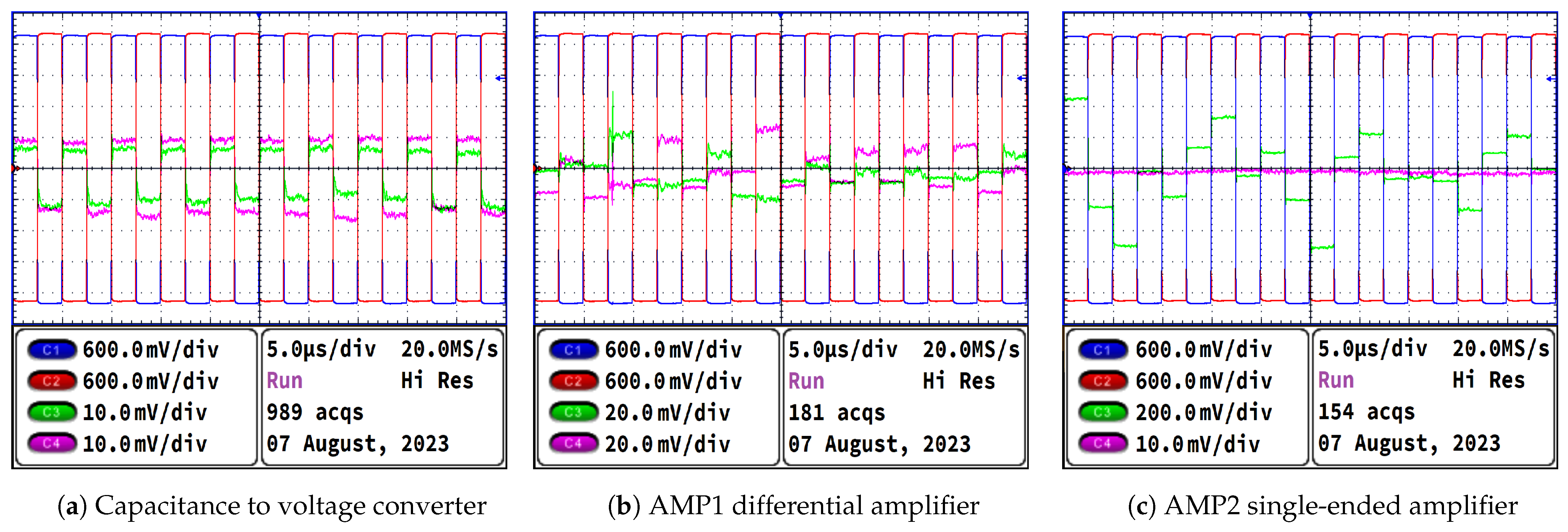
Electronics 13 02599 g022
Figure 23. Clock signals (red and blue) and analog voltages at outputs of signal processing blocks: differential (green and violet) outputs of the C2V and AMP1 and single (green) output of the AMP2.
Electronics 13 02599 g023
Figure 24. Readout standard deviation measured with an oscilloscope for the ROIC #4 and ROIC #6 setups.
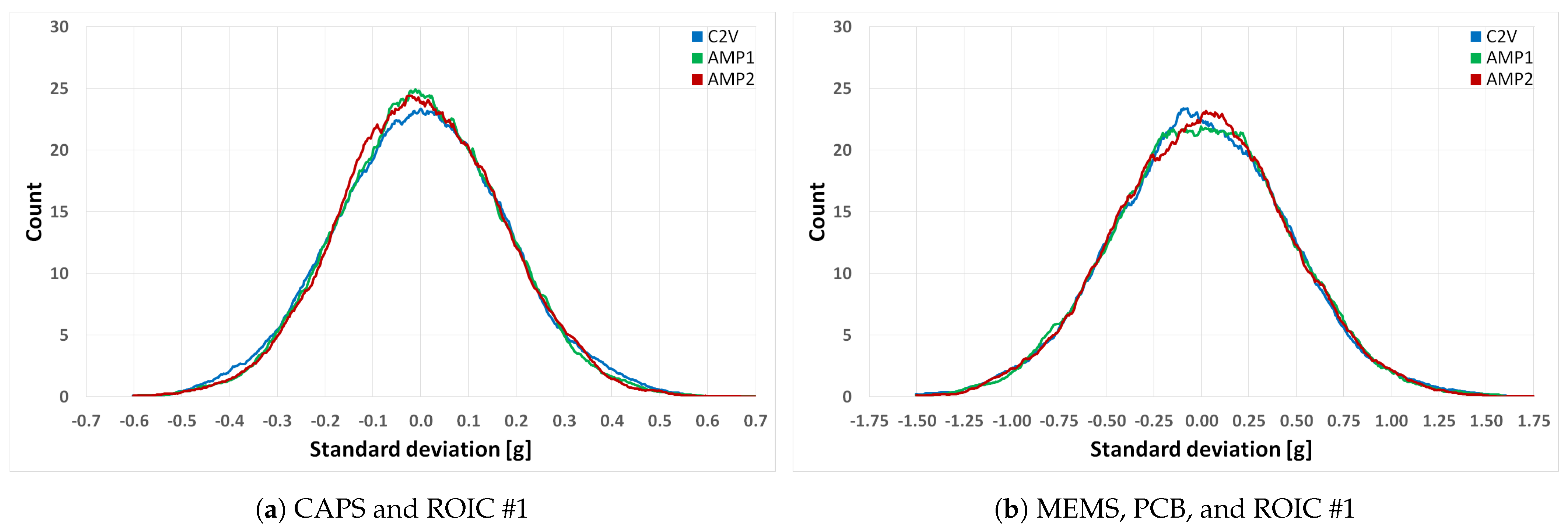
Electronics 13 02599 g024
Figure 25. Readout standard deviation measured with an oscilloscope for the CAPS and ROIC #1 and MEMS, PCB, and ROIC #1 setups.
Electronics 13 02599 g025
Figure 26. Noise amplitude spectral density measured with an oscilloscope for the ROIC #4 and ROIC #6 setups (blue curve). The orange curve shows the moving average of 100 samples for the same data.
Electronics 13 02599 g026
Figure 27. Noise amplitude spectral density measured with an oscilloscope for the CAPS and ROIC #1 and MEMS, PCB, and ROIC #1 setups (blue curve). The orange curve shows the moving average of 100 samples for the same data.
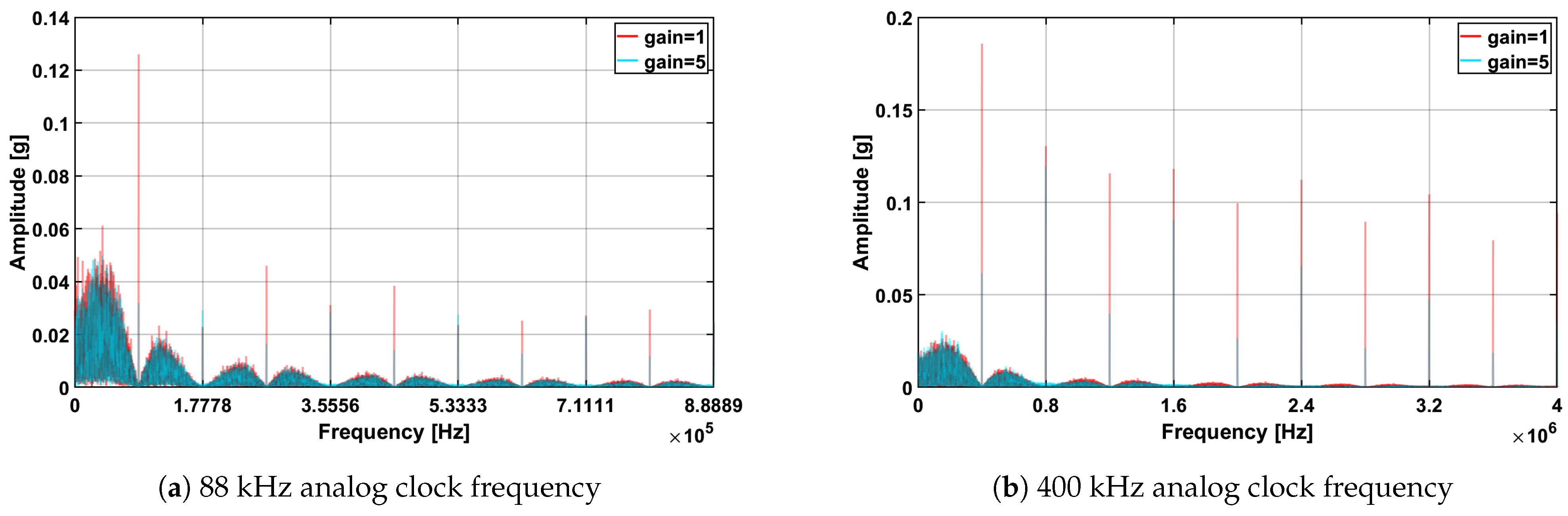
Electronics 13 02599 g027
Figure 28. FFT of the AMP2 output waveform (input of the built-in ADC) for the M&P&R #1.
Electronics 13 02599 g028
Figure 29. FFT of the AMP2 output waveform (input of the built-in ADC) for ROIC #4 and ROIC #6 at 200 kHz analog clock frequency.
Electronics 13 02599 g029
Figure 30. FFT of the AMP2 output waveform (input of the built-in ADC) for CAPS and ROIC #1 and MEMS, PCB, and ROIC #1 at 200 kHz analog clock frequency.
Electronics 13 02599 g030
Figure 31. Envelopes of readout distributions for MEMS, PCB, and ROIC #1 for several operation modes of the thermal chamber.
Electronics 13 02599 g031
Figure 32. Power spectral density of the thermal chamber during different operation phases.
Electronics 13 02599 g032
Table 1. Parameters of the designed capacitive MEMS accelerometer (X axis).
ParameterValue
Sensor horizontal (frame) size1300 μ m
Sensor vertical (frame) size930 μ m
Active layer thickness30 μ m
Finger length210 μ m
Finger width4 μ m
Number of finger pairs (top + bottom part)160
Finger’s spacing2 μ m
Initial capacitance (top or bottom part)3.07 pF
Sensitivity13.15 fF/g
Suspension stiffness29.60 N/m
Movable part volume11.17 ×   10 3 mm3
Movable part mass26.03 ×   10 9 kg
First resonant frequency5.32 kHz
Q factor26.22
Table 2. Calculated and measured noise levels from different sources.
MEMS and ROIC [ μ g/ H z ]ROIC Only [ μ g/ H z ]
Amplifier noise80.640.8
Switch noise14.214.2
Voltage reference noise5.55.5
Brownian noise3.10
Total calculated noise from above sources82.143.6
Total simulated noise248123
Total measured noise839303
Table 3. Explanation of the test setup naming convention and composition (including ROIC, MEMS, ROIC and MEMS, and PCB specimens).
Test Setup NameMEMS/ROIC Specimen Utilized in the SetupPCB Specification: Type, Version, and SpecimenRemarks
MEMS and ROIC #1MEMS and ROIC #11× QFN 1, ver. 1, spec. 1
MEMS and ROIC #2MEMS and ROIC #21× QFN, ver. 2, spec. 1
MEMS and ROIC #3MEMS and ROIC #3Socket 2, ver. 1, spec. 1
MEMS and ROIC #5MEMS and ROIC #5Socket, ver. 1, spec. 1
MEMS, PCB, and ROIC #1ROIC #7 and MEMS #112× QFN 3, ver. 1, spec. 3
ROIC #1ROIC #12× QFN, ver. 1, spec. 1
ROIC #2ROIC #22× QFN, ver. 2, spec. 1The same PCB as ROIC #3
ROIC #3ROIC #32× QFN, ver. 2, spec. 1The same PCB as ROIC #2
ROIC #4ROIC #42× QFN, ver. 2, spec. 2
ROIC #5MEMS and ROIC #3Socket, ver. 1, spec. 1MEMS and ROIC disconnected
ROIC #6ROIC #62× QFN, ver. 1, spec. 4
CAPS and ROIC #1ROIC #62× QFN, ver. 1, spec. 4Capacitors at ROIC #6 inputs
1 PCB for MEMS and ROIC dies in a single QFN-100 package. 2 PCB with the test socket for a single QFN-100 package. 3 PCB for MEMS and ROIC dies in two separate QFN-100 packages.
Table 4. Progression of the standard deviation of signals processed in the analog readout path and at the output of the internal ADC.
Test Setup NodeASIC.4 [g]ASIC.6 [g]CAPS and ROIC #1 [g]M&P&R #1 [g]
C2V0.16010.18080.17760.4584
AMP10.14510.16910.17060.4566
AMP20.15370.17150.16860.4505
ADC0.16910.17770.17840.4682
Table 5. Progression of the standard deviation of signals processed in the analog readout path and at the output of the internal ADC.
Test Setup NodeASIC.4 [mV]ASIC.6 [mV]CAPS and ROIC #1 [mV]M&P&R #1 [mV]
C2V3.0153.3983.3398.617
AMP110.91012.71512.82834.333
AMP211.55712.89612.67833.875
ADC12.71513.36213.41535.206
Table 6. Progression of standard deviation of signals processed in analog readout path in millivolts (simulation).
Test Setup NodeNo Input Cap. [mV]3 pF Input Cap. [mV]3 pf/18 pF Input Cap. [mV]
C2V0.72131.26912.6015
AMP12.99065.138910.4410
AMP23.08165.191310.4653
Table 7. Progression of standard deviation of signals processed in analog readout path scaled in g units (simulation).
Test Setup NodeNo Input Cap. [g]3 pF Input Cap. [g]3 pf/18 pF Input Cap. [g]
C2V0.03840.06750.1384
AMP10.03980.06830.1389
AMP20.04100.06900.1392
Table 8. Dependence of readout standard deviation on MEMS excitation voltage for two different test setups.
Modulation Voltage [V]Standard Deviation [g]
00.2552
0.50.4192
1.00.4551
1.50.4541
2.00.4589
2.50.4546
3.00.4597
Table 9. Dependence of readout standard deviation on analog clock frequency for MEMS, PCB, and ROIC #1.
Test Setup MeasurementMEMS, PCB, and ROIC #1 OscilloscopeMEMS, PCB, and ROIC #1 ADCMEMS and ROIC #1 ADC
Clock [kHz]
880.46060.45580.4705
1000.45530.46550.5077
1140.45950.46570.4934
1330.45880.46490.4889
1600.46030.46070.4605
2000.46040.46250.4908
2660.45830.79470.9158
4000.45930.82460.8310
Table 10. Dependence of the readout standard deviation on the operation phase of the thermal chamber for the two different test setups.
Test SetupOffIdleFanActivationCompressor
MEMS, PCB, and ROIC #10.47650.46080.45960.45590.4567
MEMS and ROIC #70.47650.47680.46440.47860.4729
Disclaimer/Publisher’s Note: The statements, opinions and data contained in all publications are solely those of the individual author(s) and contributor(s) and not of MDPI and/or the editor(s). MDPI and/or the editor(s) disclaim responsibility for any injury to people or property resulting from any ideas, methods, instructions or products referred to in the content.

