Article

Leakage Power Attack-Resilient Design: PMOS-Reading 9T SRAM Cell

by
Muyu Yang
,
Prakash Balasubramanian
,
Kangqi Chen
and
Erdal Oruklu
*
Department of Electrical and Computer Engineering, Illinois Institute of Technology, 3301 S. Dearborn St., Chicago, IL 60616, USA
*
Author to whom correspondence should be addressed.
Electronics 2024, 13(13), 2551; https://doi.org/10.3390/electronics13132551
Submission received: 11 June 2024 / Revised: 27 June 2024 / Accepted: 27 June 2024 / Published: 28 June 2024
(This article belongs to the Special Issue Embedded Systems and Microcontroller Smart Applications)

Abstract

:
Non-invasive side-channel attacks (SCAs) based on leakage power analysis (LPA) have received more attention recently, since leakage current has gradually become more dominant with further scaled technologies. For SRAM cells, LPA exploits the correlation between data in memory cells and their corresponding leakage power. This paper proposes a novel SRAM design in 7 nm node for countering LPA attacks, based on a single-ended PMOS-reading 9T (nine-transistor) cell design. The leakage current imbalance, delay, stability, and robustness of SRAM cells are examined for the proposed memory cell architecture with layout designs, and results are compared against other SRAM cell designs. Simulation results and failure of LPA attacks in case studies confirm the enhanced resilient behavior for the new SRAM cell design.

1. Introduction

Non-invasive side-channel attacks (SCAs) pose a serious threat against crypto-systems [1]. For example, symmetric key encryption algorithms such as DES [2], AES [3], and Blowfish [4] utilize S-boxes (substitution boxes) for non-linear substitution operations, and S-boxes have been shown to be vulnerable against SCAs. This attack method does not have to tamper with the circuit but only observe its physical characteristics under normal operation mode [5]. An SCA normally starts from two paths: measurement of certain characteristics that could be deduced from the object hardware, and estimation based on models built for this sort of characteristics. The characteristics are measurable parameters such as power consumption or execution time [6]. Next, combining the measurement results and estimation numbers, the best match can identify the correct key [7]. In the past, differential power analysis (DPA) attacks were the primary power-based SCA threats for integrated circuits [8,9]. More recently, analysis of leakage current is proven to be capable of disclosing hidden data effectively. This sort of SCA is named a leakage power analysis (LPA) attack [10]. Works such as [11] demonstrate successful LPA attacks implemented on DPA-resilient logic.
The SRAM (static random access memory) cell, mostly used as the central processing unit (CPU) cache, plays an important role in CPU design [12]. It occupies a large area of a single chip [13], and normally a large portion of its cells remain in standby. Therefore, the SRAM is one of the major targets of LPA attacks. In particular, SRAM arrays are implemented in crypto-systems such as IoT devices [6], smart cards [14], wireless networks [15], and many other FPGA applications [16]. Based on previous attack assumptions and countermeasures [17,18], R. Giterman et al. modified the conventional 6T (six-transistor) cell design into an 8T (eight-transistor) design to eliminate data dependency and make it immune to the LPA threat [19]. S. F. Naz et al. further changed the 8T design and proposed a split 8T SRAM cell to overcome the half-select issue [20]. R. Giterman et al. introduced a low-cost impedance randomization unit to conventional 6T SRAM macrocells to counter LPA attacks [21]. The conventional 6T SRAM cell design has several problems, including stability degrading, when scaled technology is applied. Many novel designs have been proposed, such as using one of the following: a single bitline, credited for lower bitline power consumption [22]; a read-decoupling scheme, enhancing the static noise margin (SNM) under extremely low power supply [23]; and stacked access transistors, providing a further reduced leakage solution [24]. A FinFET-based power-gated nine-transistor (PG9T) cell design in [25] combines all the benefits above. Integrating the modern cell design with the SCA-resistant methodology, we can achieve the security goals and better SRAM performance simultaneously.
In this paper, we introduce a novel SRAM cell named PMOS-reading nine transistor (PR9T), with benefits inherited from the PG9T design [25] and the leakage-balancing method in [19]. The conventional 6T and PG9T designs are investigated for an in-depth performance comparison. An earlier version of the cell design we proposed, and leakage-balanced 10T (LB10T) was presented in [26]. Compared to the LB10T, the PR9T SRAM cell can achieve more reliable leakage data independence. All the circuit simulations are based on a 7 nm process design kit, ASAP7 [27], supporting multiple transistor selections in terms of threshold voltage ( V t h ) and corner models. Table 1 shows the threshold voltages of different corners and different drive strengths of NMOS and PMOS devices. Furthermore, 8 × 8 cell matrix layouts of both PR9T and PG9T cells are designed for parasitic parameter extraction to obtain accurate measurement results.

2. Related Work

The power-gated 9T (PG9T) SRAM cell design [25] targets low power dissipation with improved operating stability. The  PG9T cell is analyzed in this section to highlight its performance when using ASAP7 devices. In Figure 1, modifications can be seen compared to the 6T cell. Here, only one bitline is applied instead of two for lower power constraints. Two power-gated transistors, PGP and PGN, assist for write disturbance elimination, and they are turned off during the write process. WL is the row wordline and WWL is the column write wordline. WLPU and WLPD turn off the pass-gate transistors during the write operation. A read-decoupled scheme is enabled by MDR and signal, VVSS, to improve the read SNM. In this work, a unique single-ended sense amplifier (Figure 2) [28] is chosen for data output. Signal/SAE is manually set to fit in the clock range here for simplicity.

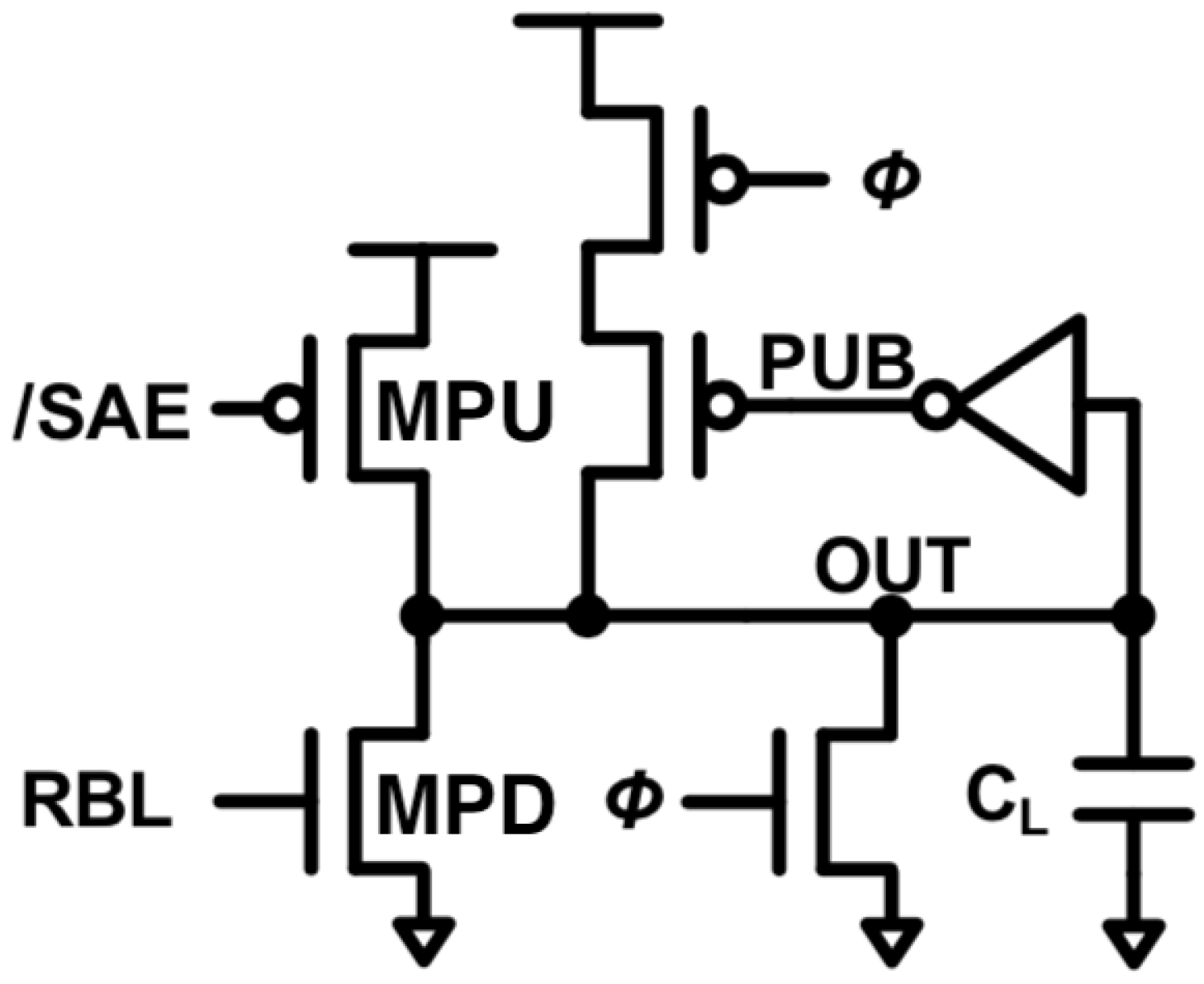
2.1. Comparison with the Conventional 6T Design

The PG9T always consumes less energy than the conventional 6T in an active case. The major reason for this power reduction is the use of one bitline in the PG9T instead of a dual-bitline design. Each bitline normally holds a high capacitance from the large number of memory cells attached to it. Using a single bitline significantly reduces the charging and discharging of nodes.
Regarding the leakage power consumption, the PG9T holds an advantage over the 6T design in restricting the subthreshold current for both data levels. Higher threshold choices lead to less power consumption under same supply voltage for both designs, as expected. According to [25], the stacked write access transistors result in a stack effect and reduced leakage for the PG9T. Again, the asymmetrical structure of the PG9T design results in imbalanced leakage performance.
The PG9T also has the advantage of much higher RSNM. The conventional 6T does not have the special transistor, MDR, to maintain stability as the PG9T does for the reading process. The HSNMs for both designs are identical in all circumstances. With the RVT and SRAM models, the reading noise margins for the PG9T are twice as large compared to a 6T cell.
Detailed simulation results for the power, delay, and noise margin are presented in Section 5.

2.2. PG9T Leakage Analysis

When an SRAM cell is in an unselected row but in a selected column for writing (i.e., write operation on a different row), leakage differs whether the data level is the same as the voltage level at bitline or not. In order to obtain this scenario to analyze the potential LPA resilience for a PG9T cell, we first need to identify a set of fixed inputs (WWL = 1, WL = 0, WLPU = 0, WLPD = 1, VVSS = 1). Unlike the conventional 6T cell, which has a symmetric design, writing 0 or 1 cannot be treated as the same for the PG9T and should be considered separately. Only a PG9T cell with fin set 123 will be discussed here. The supply voltage is 0.7 V as recommended in the PDK [27].
Figure 3 presents the scenario of writing 0. In this case, a cell holding data 0 or 1 has the same number of transistors that have leakage currents. The three leaking transistors are circled in red for holding 0 or blue for holding 1. As shown in Figure 4, the situation for writing 1 to a PG9T is quite different. For the cell holding 0, only two devices circled in blue in the cross-coupled inverters have leakage compared to four devices circled in red when the cell is holding 1. Moreover, the stacked AC1 and MDR both have major subthreshold leakage current when the cell is holding 0, and the stack effect happens here, which can reduce leakage. Overall, it can be seen that the writing-0 case may be balanced by default, while the writing-1 case suffers from a skewed number of transistors with leakage for cells holding 0 or 1.
Simulation results from single-cell experiments, shown in Table 2, confirm the analysis above. Here, the leakage ratio indicates the ratio of leakage power consumptions between cells holding 0 and 1. In the case of writing 0, the leakage ratio is close to 1 in the SLVT, LVT, and RVT models for all process corners, which meets our expectation that the leakage for holding 0 and 1 when writing 0 is the same due to the same number of transistors with leakage. In the case of writing 1, leakage ratios are skewed, with more leakage occurring when holding 1.
Table 3 shows simulation results with an 8 × 8 memory cell matrix. From the leakage ratios, it can be seen that the writing-0 or -1 behavior with SRAM-type devices changes with further deteriorated leakage balance; while SLVT devices can reach a ratio of around 1.15 for the writing-1 scenario, SRAM devices obtain a ratio as low as 0.59. Consequently, this inconsistency due to V t h variation makes it even harder to find an optimum solution for leakage balancing with PG9T cells.

3. Proposed Work

In this section, a novel SRAM cell design, PMOS-reading 9T (PR9T), is presented in order to address leakage power analysis attacks.

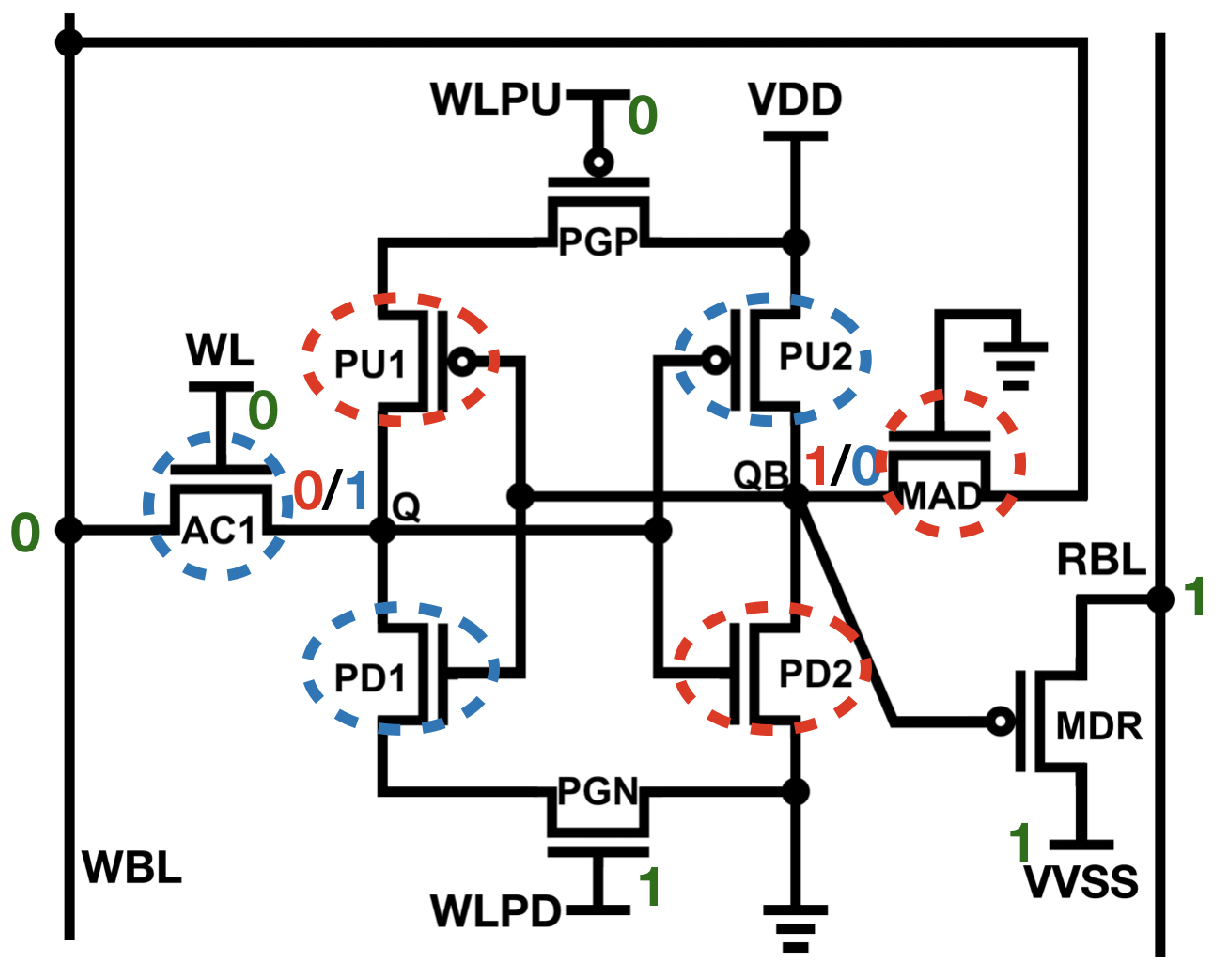
3.1. PMOS-Reading 9T Design

The schematic of the proposed PR9T cell is shown in Figure 5. From the analysis provided in the previous section, the PG9T cell is vulnerable when the attacker chooses writing 1 for LPA due to differences in leakage. Adding always-sleep transistors would reduce the imbalance without damaging functionality but increase leakage power consumption. The gate-grounded transistor MAD in the PR9T offers such a function. With its source connected to QB and its drain connected to WBL of the cell, the MAD is assured to have subthreshold leakage when QB = 0 and WBL = 1 or when QB = 1 and WBL = 0. Additionally, the stacked access scheme is removed in the PR9T for simpler leakage manipulation, but the power-gated transistor pair is not removed and still works as in the PG9T cell so that write robustness will not be affected. Since AC2 no longer exists, the writing performance could be even faster than the PG9T.
The decoupled read scheme for a high RSNM is changed. Instead of an NMOS with node Q as the gate trigger, the read scheme is moved to the QB side and uses a PMOS with node QB as its gate trigger. The PMOS transistor, MDR, acts as a switch here to choose whether the status of VVSS is passed or not. A PMOS transistor, instead of an NMOS transistor, is used here due to PMOS having a stronger ability to pass 1. Using PMOS also diminishes the leakage impact from the read scheme due to the lower leakage of PMOS over NMOS. Moreover, the reading process is separated from the writing process by two individual bitlines, WBL and RBL. Each bitline connects to the same write circuitry and sense amplifier as used in the PG9T. WL is assigned to be inserted only when writing is being processed. VVSS retains its behavior, turning logic low only if reading is in progress.
In Figure 6, the layout of a single cell of the PR9T is shown. FinFET architecture enables transistor sizing by selecting the fin number (NFIN) rather than changing the width/length ratio. Similar to [27], four options for transistor sizing were used, 111, 112, 122, and 123, with each number denoting the number of fins for pull-up (PU), access (PG), and pull-down (PD) devices. Power-gating devices are configured to be the same as pull-up or pull-down transistors.
To exhibit an intuitive view, some layers, namely, SDT, Nselect, and Pselect, are omitted, and only the necessary connections between the source, drain, and gate of each transistor are displayed. The PR9T cell layout has three metal layers. The widths of a PR9T with fin sets 111, 112, 122, and 123 are 15, 17, 19, and 21 fin pitches, so the area of a single PR9T cell with different fin sets could be 0.066 μm2, 0.074 μm2, 0.083 μm2, and 0.092 μm2. Compared to the PG9T, the area cost of the PR9T is larger, around 11%. As shown in Figure 7, the layout design of the PR9T can be mirrored to save area. Two PR9T cells with fin set 123 are mirrored, and terminals connecting to Vdd, Vss, BL, and VVSS are shared. Dummy gates and well taps are placed on the sides.
Figure 8 exhibits an 8 × 8 matrix cell layout of a PR9T, which occupies 7.185 μm2 with X and Y dimensions of 4.752 μm and 1.512 μm, respectively.

3.2. PR9T Leakage Analysis

Figure 9 and Figure 10 present the leakage analysis of the PR9T with the same annotation used for PG9T analysis. In this design, no matter what data are presented on the WBL, there are a total of three transistors leaking. During the writing-0 process, AC1 causes leakage only when the cell holds 1. On the contrary, the always-sleep transistor MAD has leakage when the cell stores 0, which balances the leakage caused by AC1 for holding 1. The same thing happens during the writing-1 process. With this design, leakages for both data levels are theoretically configured to be identical, and there is no stack effect to be concerned about.
The simulation results with respect to the leakage ratios for different scenarios are shown in Table 4 and  Table 5. It can be seen that the PR9T is a design that is resilient against LPA attacks. In single-cell simulations, none of the available models have a leakage ratio value that jumps out of the range around 1. In particular, the cells with SLVT, LVT, and RVT models have a leakage ratio of exactly 1. The ratio results for SRAM models are much better than for PG9T. Regardless of the data stored in the cells, all design corners show almost the same leakage when the WBL provides the same data. Results in Table 5 indicate that scaling the circuit size does not affect the LPA resilience behavior of the proposed design.

4. LPA Attacks

Earlier research in [17,19] already comprehensively demonstrated an analysis of the correlation between the data stored in a 6T cell and the leakage power consumption and how it can be exploited for LPA attacks. Different leakage current levels for different stored data can be exploited under certain write operations for a single SRAM cell. Combining power measurements and the estimated values (based on the Hamming weights linked to the leakage current path), a correlation analysis can be performed between the measured and estimated leakage currents [17]. The highest correlation yields the correct key. Consequently, word-length information (secret key) sealed inside a memory array can be extracted [10]. Here, we assume that the adversary has the ability to filter out the major noise associated with the overall power consumed by other components of a chip. This is not difficult to achieve since modern memory designs often offer a separate voltage supply exclusively for memory arrays to decrease the power consumption [29].

4.1. Algorithm for the LPA Attack Mechanism

The procedure of an LPA attack mechanism is given in Algorithm 1, which consists of two phases: the collection of leakage power measurements and a correlation analysis [19].
During the first phase, steps 1 to 5 in the algorithm, the adversary collects information about the leakage power consumption of the cell array. First of all, all the rows of the array except the row that contains the secret key are written with the same data d m b i t , where d m b i t is an m-bit integer number in base 2. This step initializes the Hamming weights H w of all the rows except the secret key row to zero. Then, it keeps writing the same data d m b i t to all the rows including the secret key row while the word line is deasserted (WL = 0). After that, the leakage power consumption is measured. This procedure is repeated for all 2 m different written data, d i , i = 0, …, 2 m 1 , and the corresponding measured leakage power consumption is donated by P m e a s , i .
During the correlation analysis phase (steps 6 to 9), the adversary tries the m-bit secret key k m b i t for every possible combination (total 2 m combinations). After that, the adversary needs to calculate the Hamming weights H w , k for each guess k m b i t based on the Hamming Distance (HD) between the word value and the BL value given by
H w = H D ( B L , Q ) = i ( B L i Q i )
Then, the correlation between the measured leakage power consumptions P m e a s , i and the Hamming weights H w , k is calculated, which yields the highest correlation for the correct secret key k * .
Algorithm 1 Leakage power analysis attack algorithm
1:
for d = 0; d 2 m 1 ; d + + do
2:
   Write same data d m b i t to all rows except the secret key row
3:
   Keep writing d m b i t to all rows including the secret key row with WL = 0
4:
   Measure the leakage power consumption P m e a s , i
5:
end for
6:
for k = 0; k 2 m 1 ; k + + do
7:
   Calculate the correlation between the measured leakage power consumptions and Hamming weights H w , k
8:
end for
9:
Find k * with the highest correlation

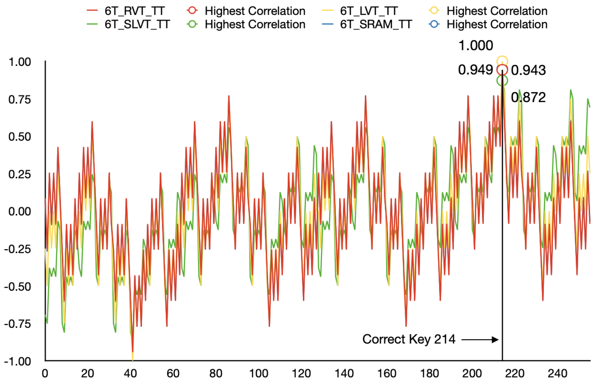
4.2. LPA Attack Results for 6T Cell and PR9T Cell

In this section, the LPA attack procedure shown in Algorithm 1 was applied to an 8 × 8 6T cell array and an 8 × 8 PR9T cell array separately. HSpice simulator was used for running all the simulations, and then simulation results were extracted by a Python script. In the last step, the Hamming weights and correlation between the Hamming weights and simulation results were calculated with another Python script.
For an example secret key of 214 ( ( D 6 ) 16 ), the results of LPA attacks with different threshold devices and the TT process corner are shown in Figure 11 for the 8 × 8 6T cell array and in Figure 12 for the 8 × 8 PR9T cell array. Figure 11 demonstrates a successful LPA attack on the 8 × 8 6T cell array, where the secret key ( D 6 ) 16 yields the highest correlation of 0.943 for RVT threshold selection; 1.000 for LVT threshold selection; 0.872 for SLVT; and 0.949 for SRAM. When considering other design corners for the 6T cell array, the highest correlations still indicate the correct secret key ( D 6 ) 16 , 0.943 for RVT, FF process corner; 0.944 for RVT, SS process corner; 1.000 for LVT, FF; 0.943 for LVT, SS; 0.864 for SLVT, FF; 0.901 for SLVT, SS; 0.947 for SRAM, FF; and 0.953 for SRAM, SS. In contrast, Figure 12 shows that the highest correlation was achieved by a wrong key on the 8 × 8 PR9T cell array when using the TT process corner. For RVT, LVT, and SLVT devices, the highest correlations are at 1.000 at ( F F ) 16 . Their patterns are similar, so they overlap in Figure 12. For the SRAM device type, the highest correlation is 0.820 at ( 29 ) 16 . None of these are the correct key. Other process corners also failed to extract the secret key for the PR9T cell.
This LPA attack procedure was repeated successfully with different secret words on the 8 × 8 6T cell array, but they all failed on the 8 × 8 PR9T cell, which demonstrates the LPA-resilient behavior of the new proposed PR9T design.

4.3. Evidence of Resilience against LPA Using Principal Component Analysis

We also investigated the resilience of the PR9T cell-based memory array against LPA attacks using principal component analysis (PCA). The test setup comprises an 8 × 8 cell array.
For each of the 256 possible secret keys, leakage measurements for all possible 8-bit data patterns are taken and stored as random variables (RVs). Thus, for an 8-bit secret key, a measurement round yields an RV comprising 256 measurements. Once leakage measurements for each of the 256 8-bit secret keys are made, they are stored in an R 256 256 data matrix. A column of this matrix corresponds to an aforementioned RV. This matrix is hereafter referred to as the measurement matrix M.
In the case of an equivalent array constructed using 6T cells, an attacker only needs one aforementioned measurement round to derive exactly one leakage measurement vector (RV). This sole leakage measurement vector is cross-correlated (Pearson correlation) with 256 leakage estimation vectors (analytically established), resulting in 256 correlation coefficients. It may be recalled that 256 8-bit secret keys are possible, resulting in 256 leakage estimation vectors. When cross-correlated with an estimation vector corresponding to the secret key, the correlation coefficient obtained is unambiguously the highest among the 256 correlation coefficients.
Instead, in the case of PR9T cells, the columns of the measurement matrix M are proven to be highly similar and hence significantly correlated by the PCA method.
Each column of matrix M is treated as a feature, and each row an observation of the feature. The covariance matrix S, meant for storing covariance among features, is computed by the following GEMM (generic matrix multiplication) operation:
S = M T M / 256
The centering and normalization of data are not required since all observation vectors represent the same exact entity (a leakage measurement).
Next, an eigenvalue decomposition of the covariance matrix S is performed, and the eigenvalues of the eigenvectors examined. Among all the eigenvalues, exactly one eigenvalue stands out and is found to be significantly higher than the rest. It is a clear indication that all columns of M are therefore similar and highly correlated. In other words, leakage is consistent and balanced regardless of the secret key and public data in the remaining cells.
Even if an attack, as described in [19], as in the case of a 6T cell is carried out, the measurement vector cannot be correlated with any analytically computed estimate because all estimates yield a constant leakage value.
The ratios between the two largest eigenvalues of S computed on four different cell types across the three process corners are presented in Table 6. A high ratio is a clear indication of a high degree of similarity and correlation among all measurements. The eigenvalue decomposition of S with measurements taken for three secret keys is presented in Figure 13 for different process corners.

5. Performance Comparison and Discussion

In this section, performance data are gathered and compared for the three types of SRAM cell designs that have been discussed: conventional 6T, power-gated 9T, and PMOS-reading 9T design. Here, 8 × 8 memory arrays are built for power measurement. The Delay and noise margins are simulated for a single cell. Parasitic parameters extracted from the layout are considered in the simulations. A fin set 123 is used for all designs. Again, the power supply is fixed at 0.7 V, and the clock frequency is 1 GHz.

5.1. Dynamic Power Consumption

Dynamic power is measured through averaging multiple iterations of writing 1 or 0 for each clock cycle. Simulation results with different threshold voltage selections and different process corners for each design are plotted in Figure 14. Overall, high-threshold-voltage transistor models result in less dynamic power consumption, as expected. It can be seen that single-ended designs provide significantly reduced dynamic power consumption compared to the dual-bitline 6T cell (as explained in Section 2). The dynamic power consumptions of the PR9T cell are similar to those in the PG9T, since the PR9T keeps the power-gated structure from the PG9T (transistors PGP and PGN), which reduces power during the writing process.

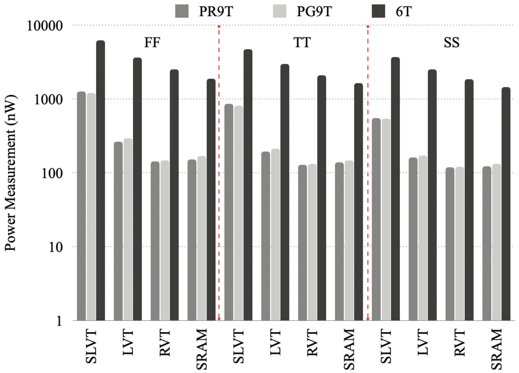
5.2. Static Power Consumption

Figure 15 presents the leakage power results. Due to large leakage variance for different V t h selections, those values are classified by the V t h model choice. As expected, although circuits with the FF process corner are fastest, the static power consumptions are also larger than the TT corner and the SS corner.
Generally, the proposed design increases the leakage over its predecessor, PG9T, because of the additional leaking transistor MAD and the absence of a stack of AC1 and MDR. Counting the leaking transistors inside the PR9T design, it can be observed that for either the holding-0 or the holding-1 case, there are exactly three transistors causing leakage, one PMOS and two NMOS devices. This reveals the LPA resistance ability of the PR9T design during standby. Its static power consumption is slightly less than the conventional 6T cell. Among these three designs, the PG9T cell has the least-static power consumption.

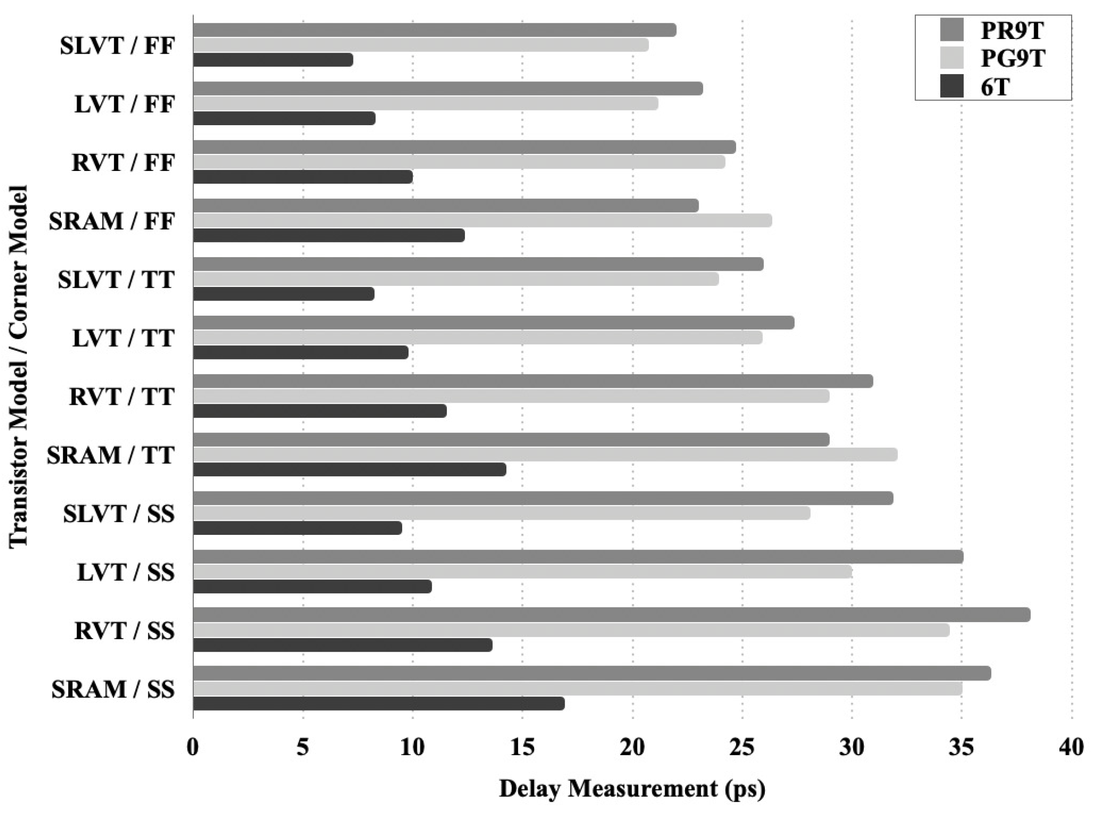
5.3. Delay Performance

Delay results are plotted in Figure 16 and Figure 17. Generally, circuits with high threshold voltage selection have larger delay, and designs with the FF process corner are faster than TT and SS, which is in accordance with expectations.
For most of the writing cases, the PR9T has the best performance among these three designs. Its predecessor, the PG9T design, has the worst delay performance for writing 0, which may be due to its two-access-transistors structure. For SLVT and LVT models, the PG9T cell achieves a much shorter delay time of writing 1 than the conventional 6T. On the other hand, for RVT and SRAM models, the 6T cell is able to obtain a faster writing-1 operation than the PG9T design. The delay performance of the writing process is similar for the 6T and PR9T when using the SRAM model. As shown in Figure 17, the 6T cell design is the fastest SRAM cell for read operations. This is partially credited to the different sense amplifiers applied in the 6T design. The PG9T is slightly faster than the PR9T in the reading process with the same sense amplifier used.

5.4. Static Noise Margin

The PR9T preserves the same read structure as in the PG9T design so that the RSNM is maintained as high as the HSNM for both designs. Simulation results prove that the PR9T has the exact same stability performance as the PG9T design. Figure 18 presents the VTC curves of the RSNM for the PR9T cell and 6T cell. The 6T cell does not have the capability to reach such a high RSNM as the PR9T design due to its conventional differential read strategy.

5.5. SRAM Model Process Corner Comparison

Finally, Table 7, Table 8 and Table 9 compare cell designs based on one single cell when using the SRAM model and highlight the performance differences for different design corners. The simulation results meet the patterns observed from results of 8 × 8 matrix cells in previous sections.

6. Conclusions

From the comparison of PG9T and 6T cell designs, the performance benefits of the single-ended cell design can be confirmed. Both static and dynamic power consumption are reduced, while robustness is improved. When LPA-resilient modifications are introduced to the PG9T cell, the new proposed PR9T cell design is obtained. The PR9T cell presents a near-perfect LPA resistance ability for both writing cases (i.e., the leakage ratios are near or exactly 1). The simulation results and LPA attack analysis demonstrate that PR9T design is a safe choice if the adversary chooses standby mode as the attacking scenario. LPA attacks on the PR9T fail, whereas these attacks are successful when applied to PG9T or 6T cells. Compared to the conventional 6T cell, the PR9T has much smaller dynamic power consumption due to the power-gated structure inherited from the PG9T. The PR9T cell also shows an advantage in leakage power consumption performance, while the area cost is around 11% larger than the PG9T. Delay for write operations is smaller for RVT-, LVT-, and SLVT-type devices and slightly slower for the SRAM-type device. The 6T cell is faster for read operations due to sense amplifier differences. Overall, single-ended designs of the PG9T and PR9T offer improved stability and noise margins compared to the 6T cell design.
For future work, we will investigate the resilience of the SRAM cells against deep learning (DL)-based side-channel attacks. Deep learning attacks using CNNs (convolutional neural networks) and MLP (multilayer perceptron) networks have been successfully used in both profiled [30,31] and non-profiled SCA attacks [32] and show superior performance compared to other methods.

Author Contributions

Conceptualization, M.Y., K.C. and E.O.; methodology, M.Y., P.B., K.C. and E.O.; software, M.Y., P.B. and K.C.; validation, M.Y., P.B. and E.O.; formal analysis, M.Y.; investigation, M.Y., P.B., K.C. and E.O.; resources, E.O.; data curation, M.Y.; writing—original draft preparation, M.Y.; writing—review and editing, E.O.; visualization, M.Y.; supervision, E.O.; project administration, E.O. All authors have read and agreed to the published version of the manuscript.

Funding

This research received no external funding.

Data Availability Statement

Data are contained within the article.

Conflicts of Interest

The authors declare no conflicts of interest.

Abbreviations

The following abbreviations are used in this manuscript:
AESAdvanced encryption standard
CNNConvolutional neural network
DESData encryption standard
DLDeep learning
DPADifferential power attack
HSNMHold static noise margin
LB10TLeakage balanced 10 transistor
LPALeakage power analysis
LVTLow-threshold-voltage transistor
MLPMultilayer perceptron
PCAPrincipal component analysis
PG9TPower-gated nine transistor
PR9TPMOS-reading nine transistor
RSNMRead static noise margin
RVTRegular-threshold-voltage transistor
S-boxSubstitution box
SCASide-channel attack
SLVTSuper-low-threshold-voltage transistor
SNMStatic noise margin
SRAMStatic random access memory

References

  1. Lerman, L.; Veshchikov, N.; Picek, S.; Markowitch, O. On the Construction of Side-Channel Attack Resilient S-boxes. In Proceedings of the International Workshop on Constructive Side-Channel Analysis and Secure Design, Paris, France, 13–14 April 2017; Springer: Berlin/Heidelberg, Germany, 2017; pp. 102–119. [Google Scholar]
  2. Biryukov, A.; De Cannière, C. Data encryption standard (DES). In Encyclopedia of Cryptography and Security; van Tilborg, H.C.A., Ed.; Springer: Boston, MA, USA, 2005; pp. 129–135. [Google Scholar] [CrossRef]
  3. Dworkin, M.; Barker, E.; Nechvatal, J.; Foti, J.; Bassham, L.; Roback, E.; Dray, J. Advanced Encryption Standard (AES); National Institute of Standards and Technology: Gaithersburg, MD, USA, 2001. [CrossRef]
  4. Schneier, B. Description of a New Variable-Length Key, 64-bit Block Cipher (Blowfish). In Proceedings of the Fast Software Encryption, Cambridge Security Workshop, Cambridge, UK, 9–11 December 1993; Springer: Berlin/Heidelberg, Germany, 1993; pp. 191–204. [Google Scholar]
  5. Tiri, K.; Verbauwhede, I. A VLSI design flow for secure side-channel attack resistant ICs. In Proceedings of the Design, Automation and Test in Europe, Munich, Germany, 7–11 March 2005; Volume 3, pp. 58–63. [Google Scholar] [CrossRef]
  6. Aamir, M.; Sharma, S.; Grover, A. ChaCha20-in-Memory for Side-Channel Resistance in IoT Edge-Node Devices. IEEE Open J. Circuits Syst. 2021, 2, 833–842. [Google Scholar] [CrossRef]
  7. Tiri, K. Side-Channel Attack Pitfalls. In Proceedings of the 2007 44th ACM/IEEE Design Automation Conference, San Diego, CA, USA, 4–8 June 2007; pp. 15–20. [Google Scholar]
  8. Kocher, P.; Jaffe, J.; Jun, B. Differential power analysis. In Proceedings of the Annual International Cryptology Conference, Santa Barbara, CA, USA, 15–19 August 1999; Springer: Berlin/Heidelberg, Germany, 1999; pp. 388–397. [Google Scholar]
  9. Kocher, P.; Jaffe, J.; Jun, B.; Rohatgi, P. Introduction to differential power analysis. J. Cryptogr. Eng. 2011, 1, 5–27. [Google Scholar] [CrossRef]
  10. Alioto, M.; Giancane, L.; Scotti, G.; Trifiletti, A. Leakage Power Analysis Attacks: A Novel Class of Attacks to Nanometer Cryptographic Circuits. IEEE Trans. Circuits Syst. I Regul. Pap. 2010, 57, 355–367. [Google Scholar] [CrossRef]
  11. Alioto, M.; Bongiovanni, S.; Djukanovic, M.; Scotti, G.; Trifiletti, A. Effectiveness of Leakage Power Analysis Attacks on DPA-Resistant Logic Styles Under Process Variations. IEEE Trans. Circuits Syst. I Regul. Pap. 2014, 61, 429–442. [Google Scholar] [CrossRef]
  12. Prasad, G.; Mandi, B.C.; Ramu, P.; Sowrabh, T.V.; Kumar, A.H. Statistical Analysis of 5T SRAM Cell for Low Power and Less Area SRAM Based Cache Memory for IoT Applications. In Proceedings of the 2020 First International Conference on Power, Control and Computing Technologies (ICPC2T), Raipur, India, 3–5 January 2020; pp. 368–372. [Google Scholar] [CrossRef]
  13. Patt, Y.N.; Patel, S.J.; Evers, M.; Friendly, D.H.; Stark, J. One billion transistors, one uniprocessor, one chip. Computer 1997, 30, 51–57. [Google Scholar] [CrossRef]
  14. Neve, M.; Peeters, E.; Samyde, D.; Quisquater, J. Memories: A Survey of Their Secure Uses in Smart Cards. In Proceedings of the Second IEEE International Security in Storage Workshop, Washington, DC, USA, 31 October 2003; p. 62. [Google Scholar] [CrossRef]
  15. Liu, W.; Luo, R.; Yang, H. Cryptography Overhead Evaluation and Analysis for Wireless Sensor Networks. In Proceedings of the 2009 WRI International Conference on Communications and Mobile Computing, Kunming, China, 6–8 January 2009; Volume 3, pp. 496–501. [Google Scholar] [CrossRef]
  16. Trimberger, S. Security in SRAM FPGAs. IEEE Des. Test Comput. 2007, 24, 581. [Google Scholar] [CrossRef]
  17. Konur, E.; Ozelci, Y.; Arikan, E.; Eksi, U. Power Analysis Resistant SRAM. In Proceedings of the 2006 World Automation Congress, Budapest, Hungary, 24–26 July 2006; pp. 1–6. [Google Scholar] [CrossRef]
  18. Rožić, V.; Dehaene, W.; Verbauwhede, I. Design solutions for securing SRAM cell against power analysis. In Proceedings of the 2012 IEEE International Symposium on Hardware-Oriented Security and Trust, San Francisco, CA, USA, 3–4 June 2012; pp. 122–127. [Google Scholar] [CrossRef]
  19. Giterman, R.; Vicentowski, M.; Levi, I.; Weizman, Y.; Keren, O.; Fish, A. Leakage Power Attack-Resilient Symmetrical 8T SRAM Cell. IEEE Trans. Very Large Scale Integr. (VLSI) Syst. 2018, 26, 2180–2184. [Google Scholar] [CrossRef]
  20. Naz, S.F.; Chawla, M.; Shah, A.P. Leakage Power Attack and Half Select Issue Resilient Split 8T SRAM Cell. In Proceedings of the 2023 21st IEEE Interregional NEWCAS Conference (NEWCAS), Edinburgh, UK, 26–28 June 2023; pp. 1–2. [Google Scholar] [CrossRef]
  21. Weizman, Y.; Giterman, R.; Chertkow, O.; Wicentowski, M.; Levi, I.; Sever, I.; Kehati, I.; Keren, O.; Fish, A. Low-Cost Side-Channel Secure Standard 6T-SRAM-Based Memory with a 1Area and Less Than 5. IEEE Access 2021, 9, 91764–91776. [Google Scholar] [CrossRef]
  22. Carlson, I.; Andersson, S.; Natarajan, S.; Alvandpour, A. A high density, low leakage, 5T SRAM for embedded caches. In Proceedings of the 30th European Solid-State Circuits Conference, Leuven, Belgium, 23 September 2004; pp. 215–218. [Google Scholar] [CrossRef]
  23. Kushwah, C.B.; Vishvakarma, S.K. A Single-Ended with Dynamic Feedback Control 8T Subthreshold SRAM Cell. IEEE Trans. Very Large Scale Integr. (VLSI) Syst. 2016, 24, 373–377. [Google Scholar] [CrossRef]
  24. Calhoun, B.H.; Chandrakasan, A.P. A 256-kb 65-nm Sub-threshold SRAM Design for Ultra-Low-Voltage Operation. IEEE J.-Solid-State Circuits 2007, 42, 680–688. [Google Scholar] [CrossRef]
  25. Oh, T.W.; Jeong, H.; Kang, K.; Park, J.; Yang, Y.; Jung, S.O. Power-Gated 9T SRAM Cell for Low-Energy Operation. IEEE Trans. Very Large Scale Integr. (VLSI) Syst. 2017, 25, 1183–1187. [Google Scholar] [CrossRef]
  26. Chen, K.; Oruklu, E. Side-Channel Attack Resilient Design of a 10T SRAM Cell in 7nm FinFET Technology. In Proceedings of the 2019 IEEE 62nd International Midwest Symposium on Circuits and Systems (MWSCAS), Dallas, TX, USA, 4–7 August 2019; pp. 860–863. [Google Scholar]
  27. Clark, L.T.; Vashishtha, V.; Shifren, L.; Gujja, A.; Sinha, S.; Cline, B.; Ramamurthy, C.; Yeric, G. ASAP7: A 7-nm finFET predictive process design kit. Microelectron. J. 2016, 53, 105–115. [Google Scholar] [CrossRef]
  28. Park, J.; Jeong, H.; Jung, S. Pulsed PMOS sense amplifier for high speed single-ended SRAM. In Proceedings of the 2018 International Conference on Electronics, Information, and Communication (ICEIC), Honolulu, HI, USA, 24–27 January 2018; pp. 1–4. [Google Scholar] [CrossRef]
  29. Qin, H.; Cao, Y.; Markovic, D.; Vladimirescu, A.; Rabaey, J. SRAM leakage suppression by minimizing standby supply voltage. In Proceedings of the International Symposium on Signals, Circuits and Systems. Proceedings, SCS 2003. (Cat. No.03EX720), San Jose, CA, USA, 22–24 March 2004; pp. 55–60. [Google Scholar]
  30. Maghrebi, H.; Portigliatti, T.; Prouff, E. Breaking Cryptographic Implementations Using Deep Learning Techniques. In Proceedings of the Security, Privacy, and Applied Cryptography Engineering, Hyderabad, India, 14–18 December 2016; Carlet, C., Hasan, M.A., Saraswat, V., Eds.; Springer: Cham, Switzerland, 2016; pp. 3–26. [Google Scholar]
  31. Benadjila, R.; Prouff, E.; Strullu, R.; Cagli, E.; Dumas, C. Deep learning for side-channel analysis and introduction to ASCAD database. J. Cryptogr. Eng. 2020, 10, 163–188. [Google Scholar] [CrossRef]
  32. Timon, B. Non-Profiled Deep Learning-based Side-Channel attacks with Sensitivity Analysis. IACR Trans. Cryptogr. Hardw. Embed. Syst. 2019, 2019, 107–131. [Google Scholar] [CrossRef]
Figure 1. Schematic of power-gated 9T SRAM Cell [25].
Electronics 13 02551 g001
Figure 2. Schematic of sense amplifier for PG9T SRAM [28].
Electronics 13 02551 g002
Figure 3. PG9T leakage analysis for writing-0 process. Red circles show transistors with leakage when the cell is holding 0, and blue circles show transistors with leakage when the cell is holding 1.
Electronics 13 02551 g003
Figure 4. PG9T leakage analysis for writing-1 process.
Electronics 13 02551 g004
Figure 5. Schematic of PR9T.
Electronics 13 02551 g005
Figure 6. Single-cell layout of PR9T with fin set 111.
Electronics 13 02551 g006
Figure 7. Mirrored two-cell layout of PR9T with dummy gate.
Electronics 13 02551 g007
Figure 8. The 8 × 8 matrix cell layout of PR9T with fin set 123.
Electronics 13 02551 g008
Figure 9. Leakage analysis of PR9T (writing 0).
Electronics 13 02551 g009
Figure 10. Leakage analysis of PR9T (writing 1).
Electronics 13 02551 g010
Figure 11. LPA attack results for the 8 × 8 6T cell array.
Electronics 13 02551 g011
Figure 12. LPA attack results for the 8 × 8 PR9T cell array.
Electronics 13 02551 g012
Figure 13. Eigenvalue decomposition of covariance matrices.
Electronics 13 02551 g013
Figure 14. Dynamic power consumption of SRAM designs.
Electronics 13 02551 g014
Figure 15. Static power (nW) consumption of SRAM cell designs.
Electronics 13 02551 g015
Figure 16. Delay (ps) comparison of SRAM cell designs (writing).
Electronics 13 02551 g016
Figure 17. Delay comparison of SRAM cell designs (reading).
Electronics 13 02551 g017
Figure 18. RSNM comparison for PR9T; furthermore, conventional 6T.
Electronics 13 02551 g018
Table 1. Threshold voltage (V) of different corners (ASAP7 PDK).
TypeCornerSRAMRVTLVTSLVT
NMOSFF0.280.200.130.07
TT0.270.190.120.06
SS0.260.180.110.05
PMOSFF−0.23−0.20−0.14−0.08
TT−0.22−0.19−0.13−0.07
SS−0.21−0.18−0.12−0.06
Table 2. Leakage ratio for single-cell PG9T circuit.
LayoutWrittenCornerThreshold Selection
SLVTLVTRVTSRAM
Pre-layout0FF1.0021.0020.9170.810
TT1.0020.9990.8730.885
SS1.0020.9950.9320.815
1FF1.3581.3691.2251.107
TT1.2971.3071.1801.099
SS1.2081.2061.1151.097
Post-layout0FF1.0030.9960.9390.734
TT1.0020.9980.9300.797
SS1.0020.9950.9660.798
1FF1.3401.3471.2240.999
TT1.2841.2931.1790.978
SS1.1901.1991.1211.261
Table 3. Leakage ratio for 8 × 8 PG9T circuit.
LayoutWrittenCornerThreshold Selection
SLVTLVTRVTSRAM
Pre-layout0FF1.0010.9910.9000.729
TT1.0010.9900.8930.751
SS1.0010.9880.8800.735
1FF1.1651.1531.0110.866
TT1.1521.1401.0000.867
SS1.1281.1140.9710.867
Post-layout0FF1.0010.9920.9050.594
TT1.0010.9910.9020.599
SS1.0010.9900.8880.650
1FF1.1541.1421.0150.739
TT1.1431.1321.0030.747
SS1.1231.1090.9790.783
Table 4. Leakage ratio for single-cell PR9T circuit.
LayoutWrittenCornerThreshold Selection
SLVTLVTRVTSRAM
Pre-layout0FF1.0001.0001.0000.909
TT1.0001.0001.0010.900
SS1.0001.0001.0010.932
1FF1.0001.0001.0000.936
TT1.0001.0001.0000.938
SS1.0001.0001.0000.938
Post-layout0FF1.0001.0001.0000.952
TT1.0001.0000.9890.869
SS1.0001.0000.9770.929
1FF1.0001.0000.9990.970
TT1.0001.0001.0000.970
SS1.0001.0001.0000.970
Table 5. Leakage ratio for 8 × 8 PR9T circuit.
LayoutWrittenCornerThreshold Selection
SLVTLVTRVTSRAM
Pre-layout0FF1.0001.0001.0000.864
TT1.0001.0001.0000.862
SS1.0001.0001.0000.861
1FF1.0001.0001.0000.911
TT1.0001.0001.0000.913
SS1.0001.0001.0000.913
Post-layout0FF1.0000.9970.9690.871
TT0.9990.9960.9850.837
SS0.9990.9930.9720.886
1FF1.0001.0000.9960.938
TT1.0000.9990.9950.942
SS1.0000.9991.0040.945
Table 6. Ratios between two largest eigenvalues of S.
CornerDevice Type
SLVTLVTRVTSRAM
FF 9.530 × 10 10 9.477 × 10 12 1.519 × 10 15 4.305 × 10 8
TT 1.430 × 10 11 1.424 × 10 13 9.498 × 10 14 1.703 × 10 8
SS 2.418 × 10 11 2.380 × 10 13 2.394 × 10 15 1.203 × 10 8
Table 7. SRAM model FF corner comparison.
ParameterPR9TPG9T6T
Leakage power
(Storing 0) (pW)
86.7282.00105.1
Leakage power
(Storing 1) (pW)
89.4482.06100.0
Dynamic power (nW)158.2146.4520.8
Delay (write 0) (ps)23.5432.5820.00
Delay (write 1) (ps)50.29112.253.48
Delay (read) (ps)23.0326.3512.37
HSNM (mV)337.6337.6337.4
RSNM (mV)337.6337.6176.7
Table 8. SRAM model TT corner comparison.
ParameterPR9TPG9T6T
Leakage power
(Storing 0) (pW)
61.6757.6773.76
Leakage power
(Storing 1) (pW)
63.5758.9970.48
Dynamic power (nW)145.4129.9438.7
Delay (write 0) (ps)28.2538.5521.23
Delay (write 1) (ps)64.77139.057.53
Delay (read) (ps)29.0032.0614.27
HSNM (mV)308.6308.6308.4
RSNM (mV)308.6308.6164.4
Table 9. SRAM model SS corner comparison.
MetricsPR9TPG9T6T
Leakage power
(Storing 0) (pW)
45.4542.8854.54
Leakage power
(Storing 1) (pW)
45.8734.0151.93
Dynamic power (nW)133.7121.1393.8
Delay (write 0) (ps)33.6843.2224.07
Delay (write 1) (ps)88.39187.965.88
Delay (read) (ps)36.3235.0116.90
HSNM (mV)267.2267.2266.5
RSNM (mV)267.2267.2143.8
Disclaimer/Publisher’s Note: The statements, opinions and data contained in all publications are solely those of the individual author(s) and contributor(s) and not of MDPI and/or the editor(s). MDPI and/or the editor(s) disclaim responsibility for any injury to people or property resulting from any ideas, methods, instructions or products referred to in the content.

