Article

Readout Circuit Design for RRAM Array-Based Computing in Memory Architecture

Zhejiang University-University of Illinois Urbana-Champaign Institute, Zhejiang University, Haining 314400, China
*
Author to whom correspondence should be addressed.
Electronics 2024, 13(13), 2478; https://doi.org/10.3390/electronics13132478
Submission received: 15 May 2024 / Revised: 6 June 2024 / Accepted: 17 June 2024 / Published: 25 June 2024
(This article belongs to the Special Issue Analog and Mixed-Signal Circuit Designs and Their Applications)

Abstract

:
In recent advancements, the traditional von Neumann architecture has been challenged by the computational needs of AI. This is due to its high power and data transfer costs. As a solution, the computing-in-memory (CIM) architecture, which combines storage and computation, has gained attention for its superior computational power and energy efficiency. Within CIM, using resistive random access memory (RRAM) arrays, the readout circuit, which converts analog outputs from multiply–accumulate operations into digital signals, faces limitations due to its area and power consumption. There are mainly two types of CIM readout circuits for analog types: the traditional ADC type and the non-traditional type. This paper presents two types of readout circuit designs. The first is a low-power, compact successive approximation register (SAR) analog-to-digital converter (ADC) readout circuit. The core circuit is an 8-bit SAR ADC operating at 70 MS/s. It incorporates a linearity-improved bootstrapped switch to minimize leakage and enhance linearity, whose spurious-free dynamic range (SFDR) has been improved by 10.1 dB from 76.78 dB to 86.88 dB, and whose signal-to-noise and distortion ratio (SNDR) has increased by 4.56 dB from 75.13 dB to 79.69 dB. The delay of a transconductance-enhanced dynamic comparator is reduced from 184 ps to 149 ps, presenting a performance improvement of approximately 20%. Concurrently, the energy consumption decreased from 178 μm to 132 μm, attaining an improvement of roughly 26%. A “sandwich” capacitor structure is used that reduces the overall area of the layout. After layout and post-simulation, this circuit occupies only 49.6 μm × 51.5 μm, consumes 553 μW power, has a SINAD of 46.22 dB, and has an SFDR of 57.21 dB. The second is a current controlled oscillator (CCO)-type readout circuit, which comprises a CCO oscillator with low process-sensitivity. The readout circuit also utilizes an op-amp and current mirrors for a negative feedback loop, ensuring a constant voltage across the RRAM arrays. The frequency generated through the CCO is controlled by the current, and quantified by a counter, supporting different weights quantification per ReRAM column without additional digital weighting. This circuit achieves 95-level resolution, 5.2 μs delay, and an average consumption of 183.1 μW. A comparative analysis highlights that traditional ADC readout circuits offer high resolution and speed but are limited by their high power and area costs, often overshadowing CIM arrays’ benefits. Thus, for applications with more lenient resolution and speed requirements, non-traditional readout circuits present considerable advantages.

1. Introduction

In the field of information technology, an AI revolution is unfolding. The computational prowess required for AI is predominantly provided by proprietary hardware chips. However, due to the deceleration of Moore’s law and bottlenecks associated with semiconductor advancement, hardware performance enhancements have not kept pace with the demands of algorithms, leading to the so-called “von Neumann bottleneck”. To transcend these constraints, various solutions, particularly CIM technology, have been proposed. CIM synergistically integrates storage and computation, thereby reducing data transfer needs. At the algorithmic level, the convolutional neural network (CNN) is suitable for feature extraction and data classification tasks. On the hardware front, RRAM displays competitive prowess within the non-volatile memory market due to its speed, low power consumption, and simplicity. Integrating RRAM into neural networks allows for the analog-domain computation of multiply-and-accumulate (MAC), mapping weight parameters to resistance values, which accelerates computing and improves energy efficiency ratios [1].
The parallel processing offered by RRAM arrays facilitates rapid and efficient data handling. Nonetheless, in certain CIM chips, the power consumption associated with the readout circuitry can be nearly 70%, while its area cost might reach up to 90%, severely constraining the energy efficiency of CIM [2]. Consequently, innovating high energy-efficient and space-conserving readout circuits becomes critical within the realm of CIM research.
There are mainly two types of CIM readout circuits for analog types: the traditional ADC type and the non-traditional type. For the first type, [3] features a variable precision circuit based on split-capacitance for 5/6 bit accuracy. This design reduces the ADC area by employing split-capacitance in the DAC and adjusting the total capacitance at the DAC output node by controlling the MSB capacitor. The authors of [4] utilize a Flash ADC readout circuit designed for 4-bit array operations. The choice of Flash ADC is attributed to its rapid speed. The strategy implements input sparsity sensing (ISS) with the Flash ADC to enhance chip energy efficiency and integration. In [5], a shared scheme is suggested where a single readout circuit is utilized across multiple columns. Further, [6] achieves a hybrid approach with analog-domain floating-point and single-slope A/D conversion to derive 2-bit exponent codes and 5-bit mantissa codes. For the second type, [7] introduces a voltage controlled oscillator (VCO)-based readout circuit, which boasts a smaller area and reduced power consumption compared to shared traditional ADC structures, making it applicable on a per-column basis. In [8], a scalable integrate-and-fire (IF) readout circuit is described, demonstrating greater suitability for spiking neural network algorithms.
This research presents the design of two readout circuit types of CIM based on RRAM arrays: a traditional ADC-based circuit and a non-traditional circuit. Section 2 outlines the design of an SAR ADC for traditional ADC readouts. Section 3 details the design of a readout circuit based on a CCO circuit. Section 4 discusses simulation results for the readout circuits described in Section 2 and Section 3. Section 5 summarizes these two types of readout circuits.

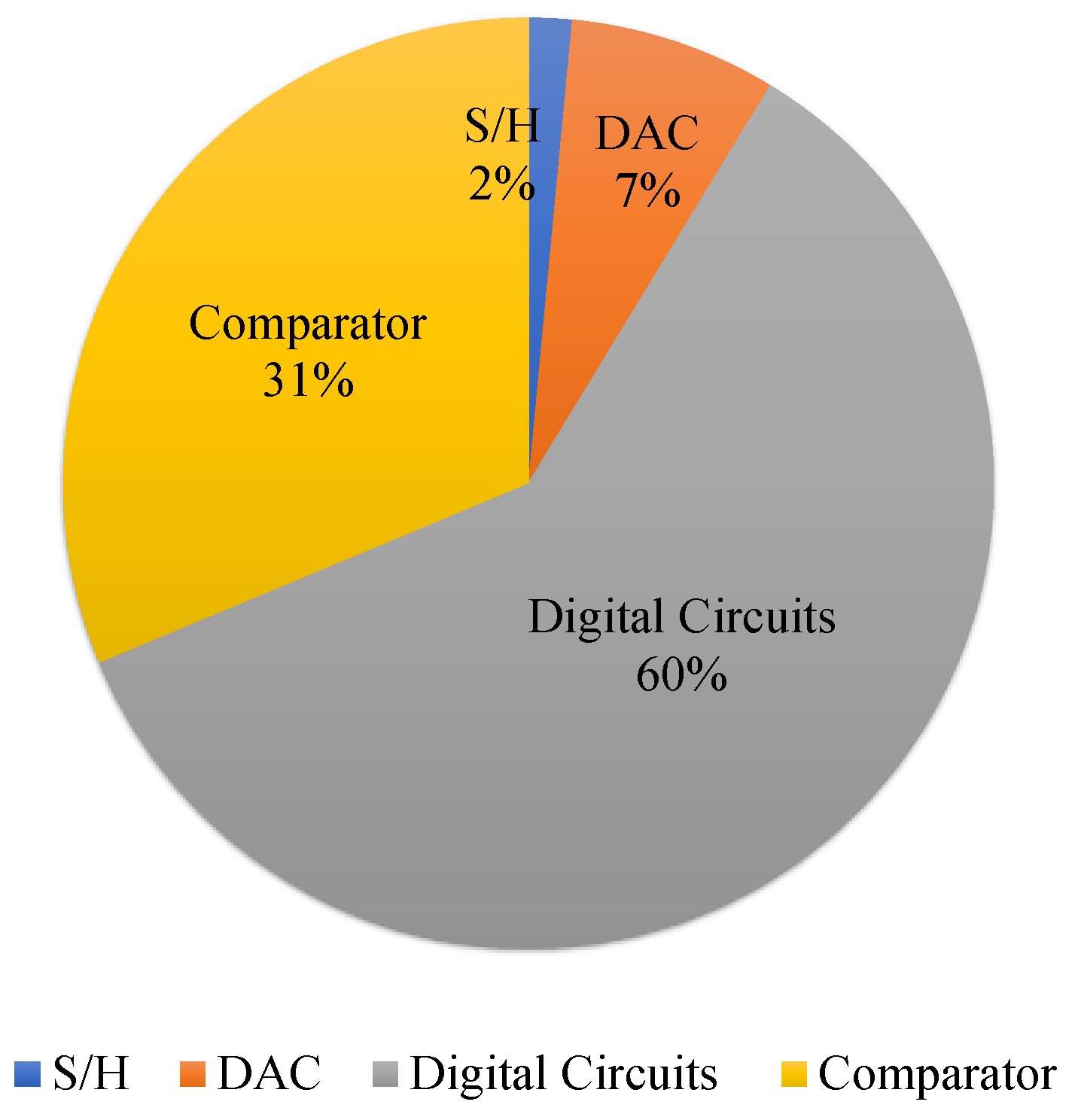
2. SAR ADC Design for Traditional ADC Readout Circuits

This section focuses on designing a low-power, compact SAR ADC architecture for traditional ADC-type readout circuits. The module converts analog voltage signals, obtained through current sampling circuits, into digital signals. Initially, we present the overall framework for an 8-bit SAR ADC, elaborating on performance metrics and key technologies related to readout circuits in CIM chips. We then detail the design process for components of the SAR ADC circuit, including the sampling switch circuit, dynamic latch comparator, DAC capacitor array.
The overall structure and timing diagram of the designed SAR ADC are as depicted in Figure 1. This includes an improved bootstrapped switch, capacitive digital-to-analog converter (CDAC) circuit, an enhanced dynamic comparator, and SAR asynchronous sequence logic. During the sampling phase, differential inputs sample on the CDAC. Triggered by the falling edge of the sampling clock, the comparator activates to retrieve the most significant bit (MSB) information. Subsequently, the MSB data are stored in the successive approximation register and used for higher-order capacitor switching in the CDAC, continuing until the least significant bit (LSB) is attained. Among them, CLKs represents the sampling period, and Clkc represents the comparison period of the comparator (in Figure 1, it is replaced by a uniform period, but in actuality, when different voltages are compared, the comparison time is different), and the change of Clkn from low level to high level represents the completion of the nth comparison.
Design highlights are shown as follows:
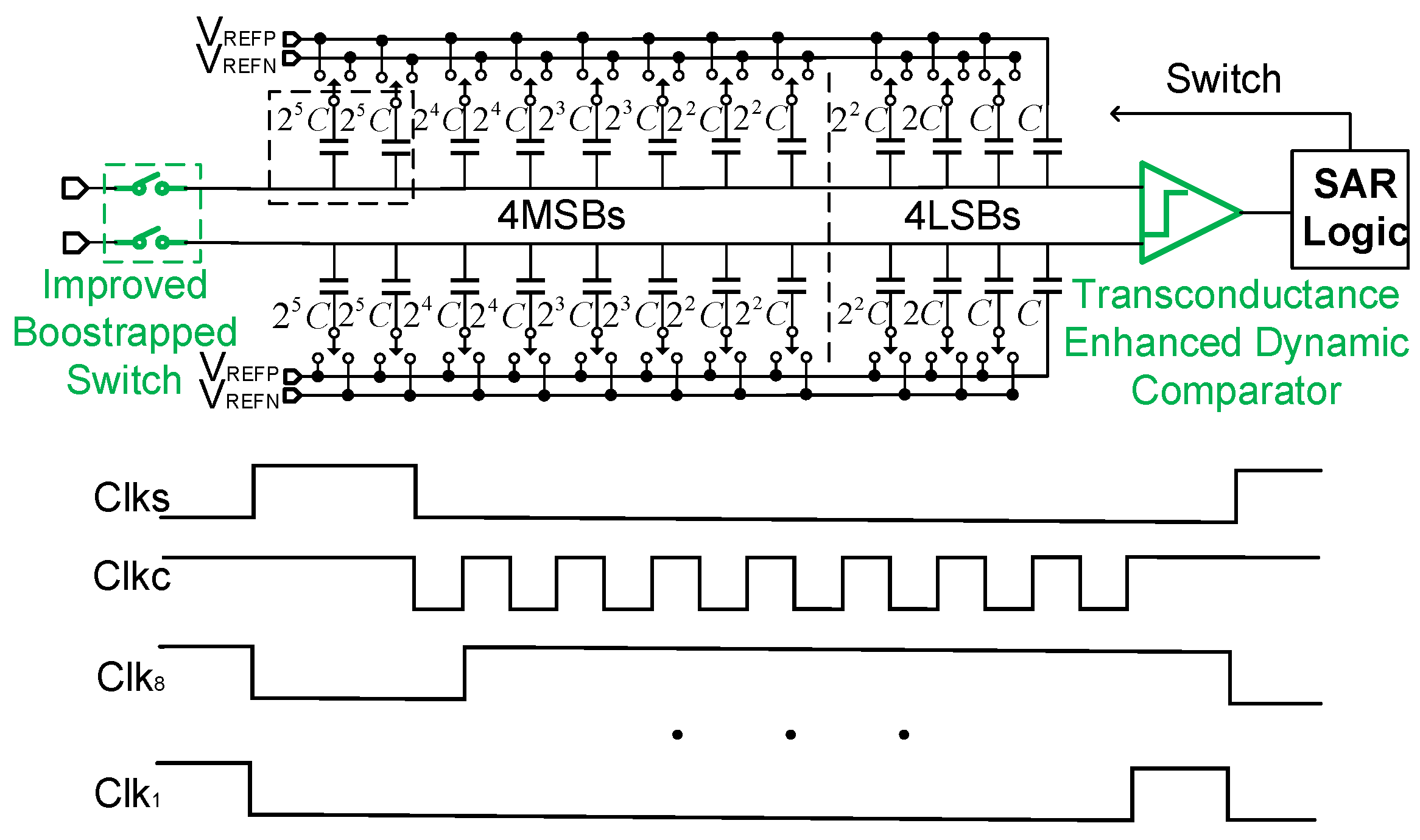
  • Improved Bootstrapped Switch: From the hold to the sampling phase, the linearity is enhanced by reducing the charge leakage related to Vin through the addition of a MOS transistor;
  • Upgraded Dynamic Comparator: During the latching phase, the comparative speed is elevated via increase in the equivalent transconductance (gm);
  • CDAC Capacitor Array: Employing a “sandwich” three-layer capacitor structure augmented with a dummy structure, this element features a minimal area and high matching precision;
  • Switching Strategy: For the top four bits, a splitting capacitor scheme is used to secure the common-mode voltage at 1/2 V r e f . The lower four bits employ a monotonic switching strategy to avoid excessive capacitor mismatches caused by excessively small unit capacitors;
  • SAR Logic: To enhance the overall comparison efficiency, we adopt an asynchronous timing scheme in SAR logic [9].

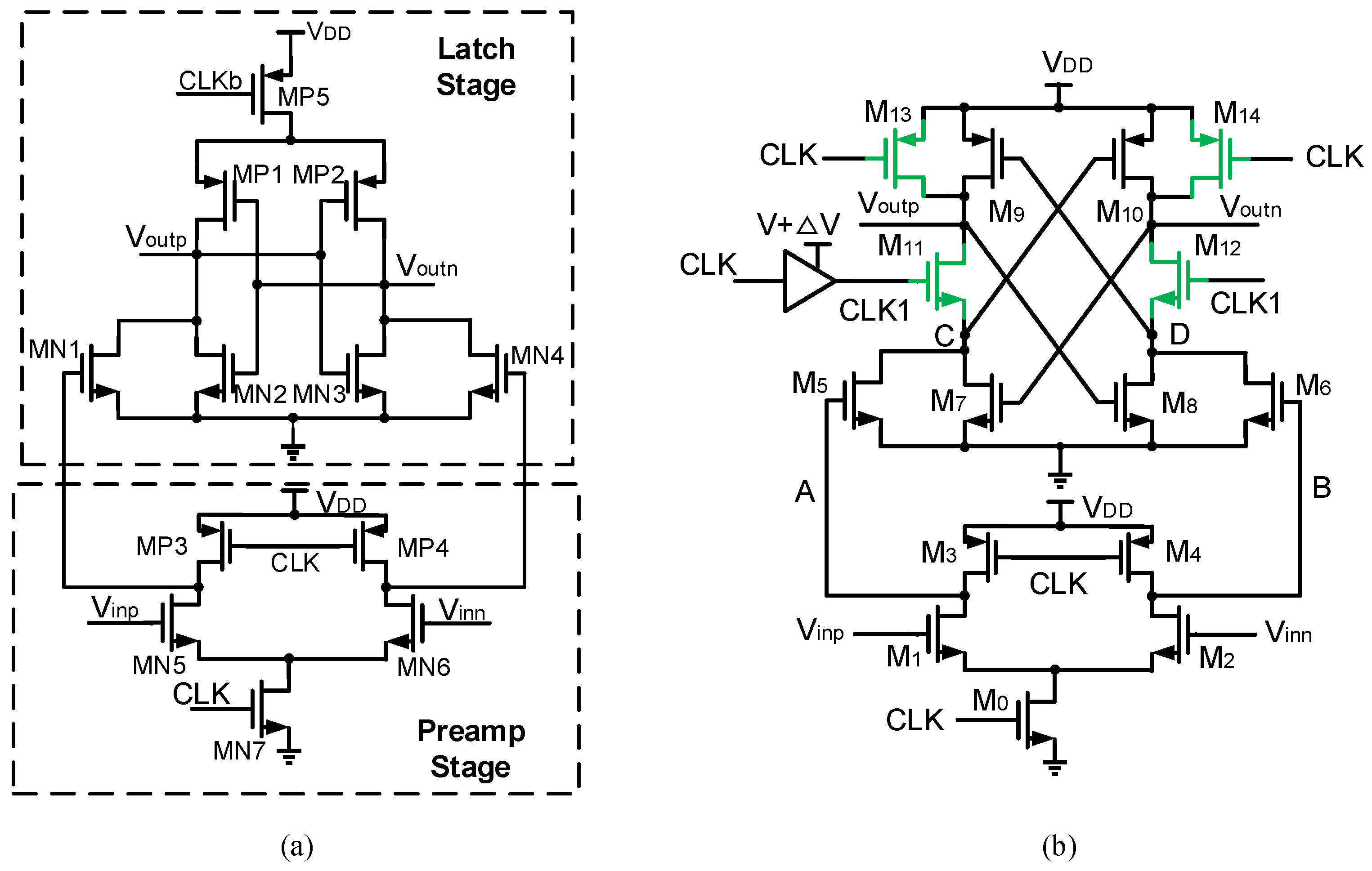
2.1. Linearity-Improved Bootstrapped Switch

To mitigate the effect of V I N variation on sampling accuracy, researchers have proposed a gate voltage bootstrapped switch that reduces the nonlinearity of the R o n . The schematic of the classical gate voltage bootstrapped switch is shown in Figure 2. When CK = 0, the switch is in the hold phase, charging the bootstrapped capacitor C B up to VDD; when CK = 1, the switch enters the sampling phase, and the gate of the sampling switch M 1 is connected to the bootstrapped capacitor C B , resulting in a gate voltage of V I N + V D D . Therefore, the gate-to-source voltage of M 1 becomes a fixed V D D , decoupling its resistance from input variations, effectively reducing switch nonlinearity and enhancing overall sampling accuracy.
The inclusion of M 4 in the classical gate voltage bootstrapped switch is to limit the V D S 5 voltage in M 5 to V X V T H 4 , preventing excessive source–drain voltage in M 5 from causing breakdown [10]. However, the introduction of M 4 introduces new nonidealities; as the mode changes from hold to sampling, the voltage at point X rises from 0 V to V X 1 due to the presence of parasitic capacitance C P , as shown in the equation below:
V X 1 = V I N + C B C B + C P V D D
C B is the bootstrapped capacitor. When M 5 is off and point Y is floating during the sampling phase, if V D D V X 1 is less than V T H 4 , M 4 does not fully turn off, causing charge to leak from X to Y. Since V X 1 is related to V I N , charge leakage becomes related to V I N , introducing nonlinearity [11].
To address the nonlinearity issue of the bootstrapped switch, an improved gate voltage bootstrapped switch is proposed, as depicted in Figure 2. This structure incorporates an additional PMOS transistor M 11 to reduce nonlinearity. During the transition from hold to sampling, M 11 is turned on, setting the voltage at point Y to V D D and ensuring V D S 4 of M 4 is much less than V T H 4 . Therefore, by turning off M 4 , the influence of V X is minimized, which, in turn, decreases the leakage from X to Y through M 4 , thereby enhancing the dynamic performance of the bootstrapped switch.
Several considerations for the gate voltage bootstrapped switch design are as follows: To achieve area optimization while ensuring stable elevation of the bootstrapped switch’s gate-to-source voltage and to fulfill the SNDR design requirement, the bootstrapped capacitor C B is set to 135 fF; other MOS transistors are sized relatively small to diminish the effects of parasitic capacitance.
The dynamic performance of the proposed linearity-improved bootstrapped sampling circuit is compared with the traditional one in Figure 3. The SFDR improved by 10.1 dB from 76.78 dB to 86.88 dB, and the SNDR improved by 4.56 dB from 75.13 dB to 79.69 dB at 70 MS/s.

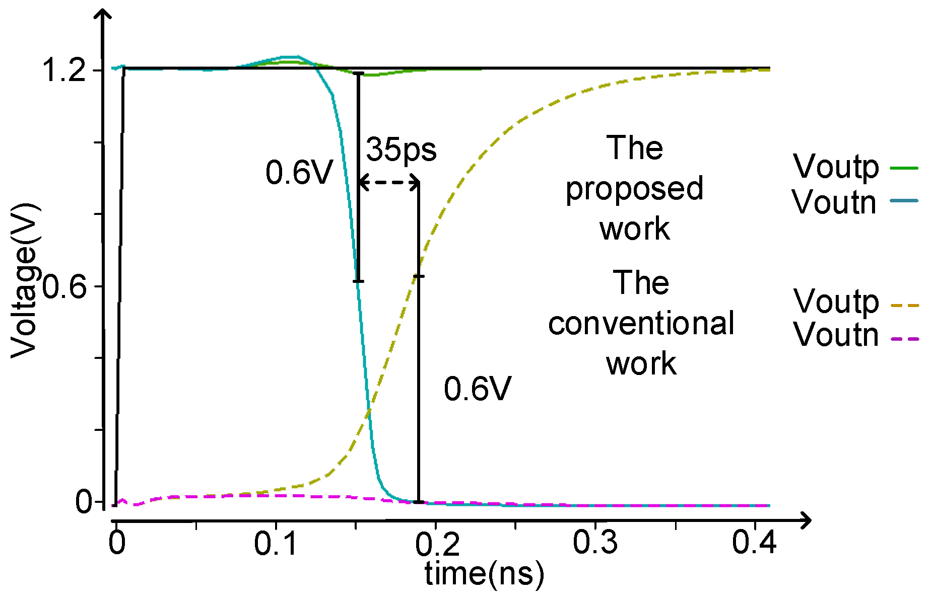
2.2. Transconductance-Enhanced Dynamic Comparator

In SAR ADC design, comparators are utilized primarily for comparing voltages across the CDAC capacitor array. Comparator designs are classified into static and dynamic types: static comparators provide lower input offset voltages with rapid response speeds, but high-resolution instances usually depend on multi-stage amplifiers, leading to high static power consumption and larger area occupancy; in contrast, dynamic comparators merge preamplification and latching stages, controlled by clock signals, typically devoid of static power consumption. Given the low energy consumption and compact size requirements of the designed readout circuit, this research opts for the dynamic comparator approach.
A traditional two-stage dynamic comparator structure is depicted in Figure 4a, comprising two operation phases: reset and compare. During reset, with CLK at low level, the comparator’s preamplification stage outputs are charged up to VDD through MP3 and MP4, activating MN1 and MN4, and grounding the output of the latching stage. In the compare phase, with CLK at high level, MN7 conducts, causing differential voltages Vinp and Vinn to discharge the preamplification stage outputs at different rates, generating a differential voltage Δ V . Concurrently, in the latching stage, MP5 conducts, allowing Δ V to propagate through MN1 and MN4 to the cross-coupled inverter structure, initiating a positive feedback mechanism. Ultimately, one high and one low level are produced at the output nodes.
The two-stage dynamic comparator, consisting of a preamplifier stage and a latching stage, allows for a flexible balance between speed and offset in low-voltage operations. During latching, the effective transconductance g m , e f f significantly influences speed. In the outlined structure, when MN2 and MN3 are off, g m , e f f is solely contributed by MP1 and MP2, affecting the comparator’s comparison speed. To achieve low power consumption and compact design in the readout circuit, while ensuring the comparator’s response speed meets specifications, a transconductance-enhanced two-stage dynamic comparator is proposed [12], illustrated in Figure 4b.
In the transconductance-enhanced two-stage dynamic comparator, the latching stage structure is improved by adding M11, M12, and M13, M14. During reset, with CLK at low, the preamplification stage functions as the conventional structure. High preamplification stage outputs lead to conduction through M5 and M6, driving M9, M10. The dual action of M13, M14 conducting sets comparator outputs V o u t p and V o u t n to high; during comparison, with CLK at high, preamplification stage outputs discharge at differing rates. As V o u t p exceeds V o u t n , point A discharges faster than B, causing M5 and M6’s V D S to diverge. High CLK1 leads to differing discharge rates at points C and D. The positive feedback formed by M7, M8, M9, and M10 ultimately sets V o u t p high and V o u t n low.
M11 and M12 ensure NMOS and PMOS (M7, M9, or M8, M10) stay in the deep inversion region during latching, thus improving g m , e f f , as shown in Equation (2):
g m , e f f = g m n + g m p = μ n C O X ( W L ) n V d s n + μ p C O X ( W L ) p | V d s p |
CLK1 is CLK plus a delay Δ t and an increased Δ V , aimed at reducing power consumption and ensuring effective conduction of M11, M12: Δ t delays M11 and M12’s conduction at CLK’s rising edge, reducing short-circuit current through M5 and M6; Δ V ensures M11 and M12 better meet V g s > V t h n . However, this structure results in longer reset times, affecting the comparator’s overall comparison speed. Thus, M13 and M14 are introduced to reduce reset time.
Comparator offset is a critical factor, particularly in terms of its evident impact on dynamic performance due to process mismatches. The transconductance-enhanced comparator runs the Monte Carlo simulation, as illustrated in Figure 5. The results indicate an average offset voltage of μ = −0.836 mV, with a standard deviation of σ = 5.03669 mV.
Waveform comparisons between the transconductance-enhanced two-stage dynamic comparator and traditional two-stage dynamic comparator are shown in Figure 6. The data indicate that for a 1 LSB input, comparator comparison delay decreased from 184 ps to 149 ps, a performance improvement of around 20%. Simultaneously, energy consumption dropped from 178 μm to 132 μm, an improvement of approximately 26%.

2.3. CDAC Switching Scheme and Unit Capacitor

To reduce the energy consumption during the switching in conventional strategies, a split-capacitor switching strategy was introduced, as detailed in [13]. This approach halves the capacitor at the most significant bit into two equal sub-capacitors, resulting in a 38% reduction in power consumption compared to traditional strategies. The monotonic switching strategy, which involves discharge only, requires 2 ( n 1 ) unit capacitors (single-ended) for an n-bit ADC, reducing the total capacitor value by half and decreasing energy consumption by 81% relative to traditional strategies. Although the monotonic strategy is efficient in saving energy, it changes the common-mode voltage of the top-plate in a differential structure. In contrast, the split-capacitor strategy maintains the common-mode voltage during switching, but the unit capacitor C u n i t used for the least significant bit is twice as much as that in the monotonic strategy.
To achieve low power consumption, reduce common-mode interference, and improve ADC accuracy, a combined switching strategy of split-capacitor and monotonic is adopted: the first four bits (MSBs) use the split-capacitor method to prevent substantial changes in the common-mode voltage during the bit variations; the last four bits (LSBs) employ the monotonic method to avoid the excessive use of C u n i t and reduce power consumption.
For a low-power, compact readout circuit applied in CIM, a “sandwich” capacitor structure is used to meet the requirements of small area, which is shown in Figure 7. The structure in SMIC 110 nm process design uses layers 4, 5, and 6, with M5 as the top plate and M4 and M6 as the bottom plate of the capacitor. To reduce the influence of parasitic capacitance on the relative accuracy of the unit capacitor, a shielding layer is added between the unit capacitors, essentially providing better protection by dummy layers and reducing capacitor mismatches at the boundaries.
The DNL and INL are estimated by the method of relative standard deviation. In the designed process, the relative standard deviation of a 10 fF MOM capacitor is 1.3%. The relative standard deviation of the designed 0.8 fF MOM capacitor can be inferred to be approximately 4.2% based on the ratio of standard deviation to capacitance [14]. As shown in Figure 8, the DNL and INL are +0.74/−0.44 LSB and +0.75/−0.73 LSB, respectively.

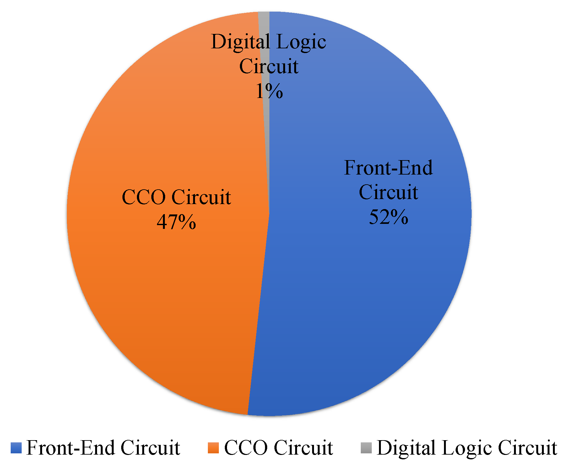
3. CCO-Type Readout Circuit
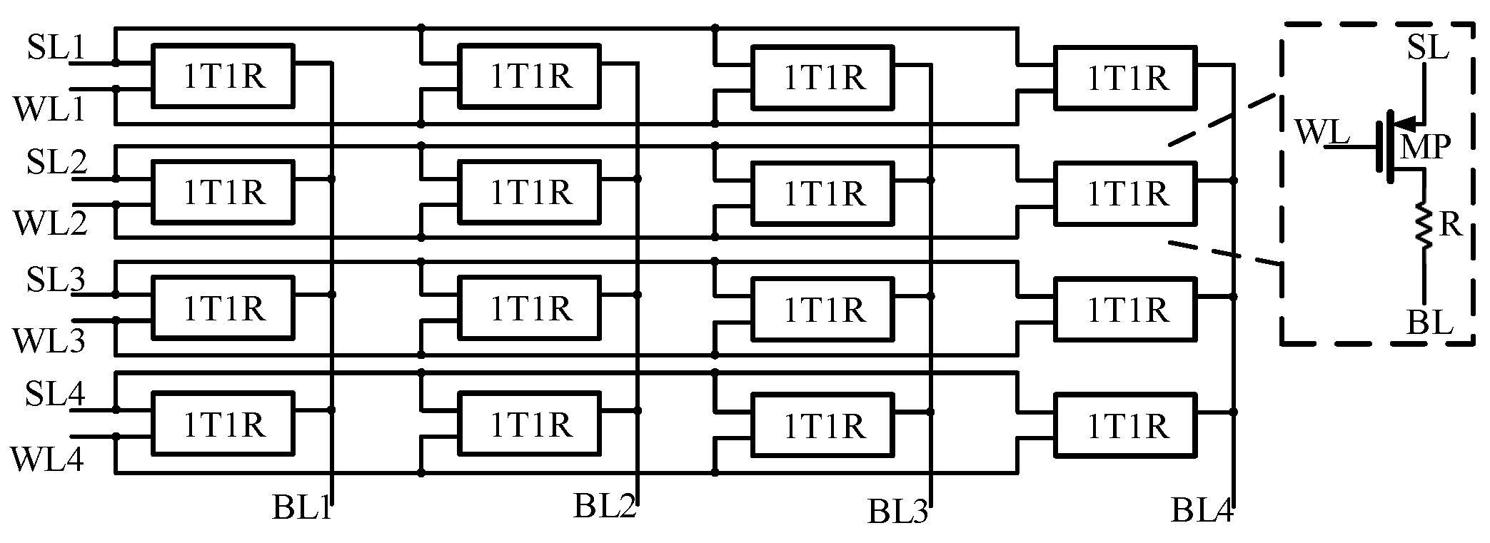
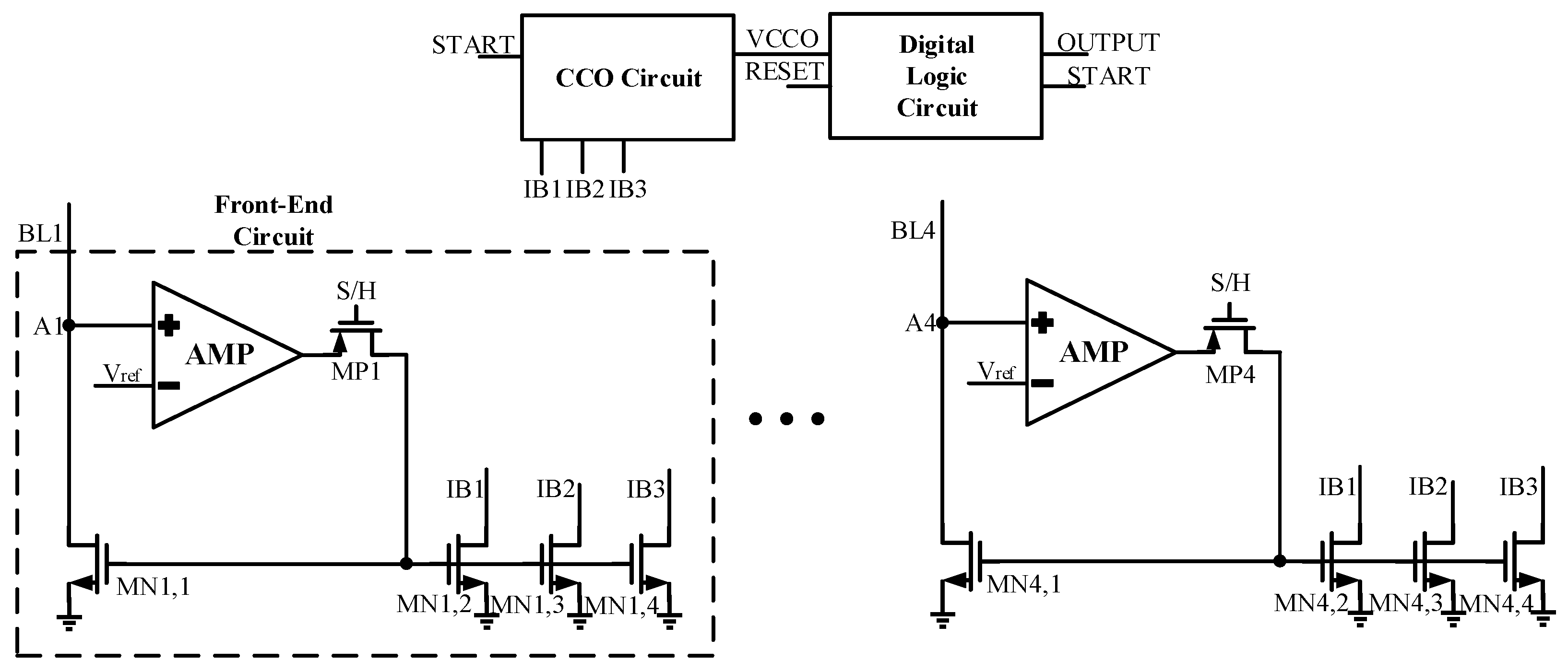
In general, the operation speed and accuracy of CIM arrays are at least an order of magnitude lower than those of the SAR ADC converters designed in Section 2. Therefore, the SAR ADC readout circuits proposed in these applications are typically utilized in shared CIM arrays, where different columns of a single CIM array or similar columns across multiple CIM arrays share a single SAR ADC readout circuit. While this type of readout circuit offers the advantage of high precision, its power consumption and area requirements are less than ideal. Hence, this section introduces a non-traditional type of readout circuit design. Leveraging the benefits of low power consumption and compact size, this readout circuit design can be applied to every column of the CIM array.
For the study of CIM readout circuits in this section, RRAM is chosen as the storage compute array element. RRAM modulates resistance through the formation and rupture of conductive filaments to enable data storage and read-write operations. The dynamism of the conductive filaments involves migration of oxygen ions and the generation and annihilation of oxygen vacancies, influenced by stochastic variations and thermal effects, leading to the switching of RRAM resistance values [15]. To simplify the model, this study adopts a linear RRAM model for designing the readout circuit, disregarding other nonlinear factors. For quantification ease, this model utilizes a dual-weight system, where high resistance states (HRS) and low-resistance states (LRS) store binary data “0” and “1”, respectively, with analog resistance using a high/low resistance ratio of 20 K Ω /2 K Ω . The 1T1R configuration is selected for simulating the array, as shown in Figure 9.
In this model, the source line (SL) connects to the transistor’s source; the bit line (BL) connects the storage unit with the column signal sensor; the word line (WL) is used for selecting the row address and triggering row signals. To use a specific 1T1R unit, the WL is enabled, and current flows out from the BL when the SL voltage is 1.2 V. A 4 × 4 CIM array constructed with 1T1R to minimize sneak current is illustrated in Figure 9. Sneak current leakage occurs when some computing units in a CIM column are disabled (SL = 0), and the current from enabled computing units (SL = 1) may flow through the BL of the disabled units and exit through SL.
The 4 × 4 CIM array’s SL1–SL4 end voltage is 1.2 V; WL1–WL4 are enabled at 0 V and disabled at 1.2 V; BL1–BL4 serve as current output ends. The readout circuit designed for the 4 × 4 CIM array, as shown in Figure 10, includes a front-end circuit, a CCO circuit, and a digital logic circuit. BL1–BL4 represent the current output from the 4 × 4 CIM array. The voltage at Point A (A1–A4) is clamped to V r e f through the operational amplifier, after which the current is mirrored into the CCO circuit (comprising three current control inverters) to produce variable frequency waveforms. Finally, a digital logic circuit quantizes waveforms of different frequencies and outputs them in digital form.
Notable design highlights within this approach include:
  • Clamp voltage
    The current within an RRAM array is computed as I = Σ V i G i . Consequently, variations in column output voltage within the CIM array induce changes in the column’s current, thus impacting accuracy. The CCO-type readout circuit designed in this paper leverages a clamping action generated by a negative feedback circuit, constructed from an operational amplifier and a current mirror, to clamp the voltage at Point A (A1–A4) to V r e f . This maintains a constant voltage difference across the array, thereby enhancing the linearity of the CIM storage compute array’s output current.
  • Selection of size in current mirror
    Given the order of magnitude variation in column current within the CIM array, careful consideration should be given to sizing MN1,1–MN4,1: these NMOS transistors must remain in the saturation region during column current changes. Therefore, prudent selection of the dimensions for these four NMOS transistors is critical during the design process. Considering the mA level current in the CIM array columns, direct replication of current via a current mirror results in prohibitive power consumption. Hence, scaling of the current is performed using (MN1,2, MN1,3, MN1,4); moreover, different proportions of (MN1,2, MN1,3, MN1,4) to (MN4,2, MN4,3, MN4,4) facilitate the assignment of varied weights to different columns within the CIM.
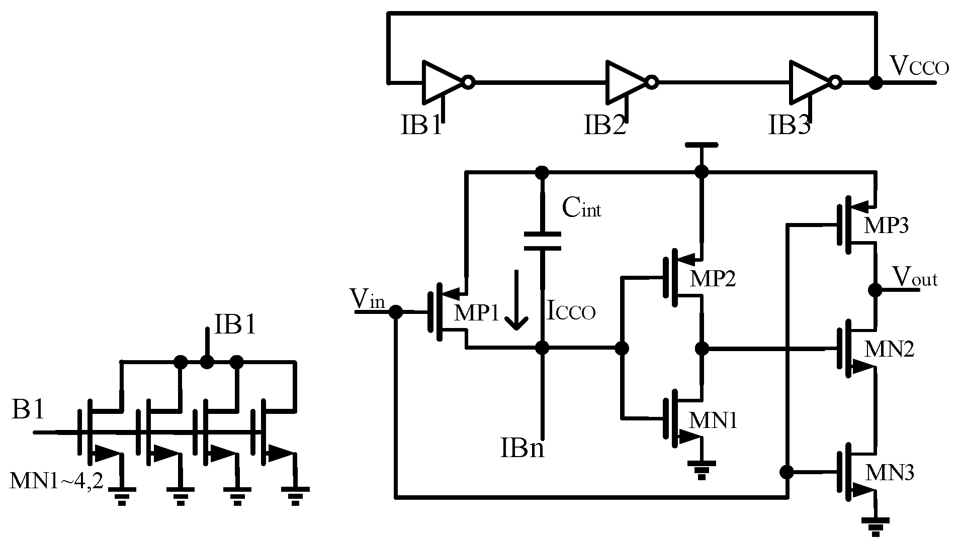
  • Design of CCO
    This study uses a design for a CCO characterized by low process-sensitivity, thereby eliminating the need for an additional reference voltage. Additionally, leveraging the complementary nature of technology-induced variations in capacitance and voltage, the design’s sensitivity to manufacturing process variations is mitigated [16].

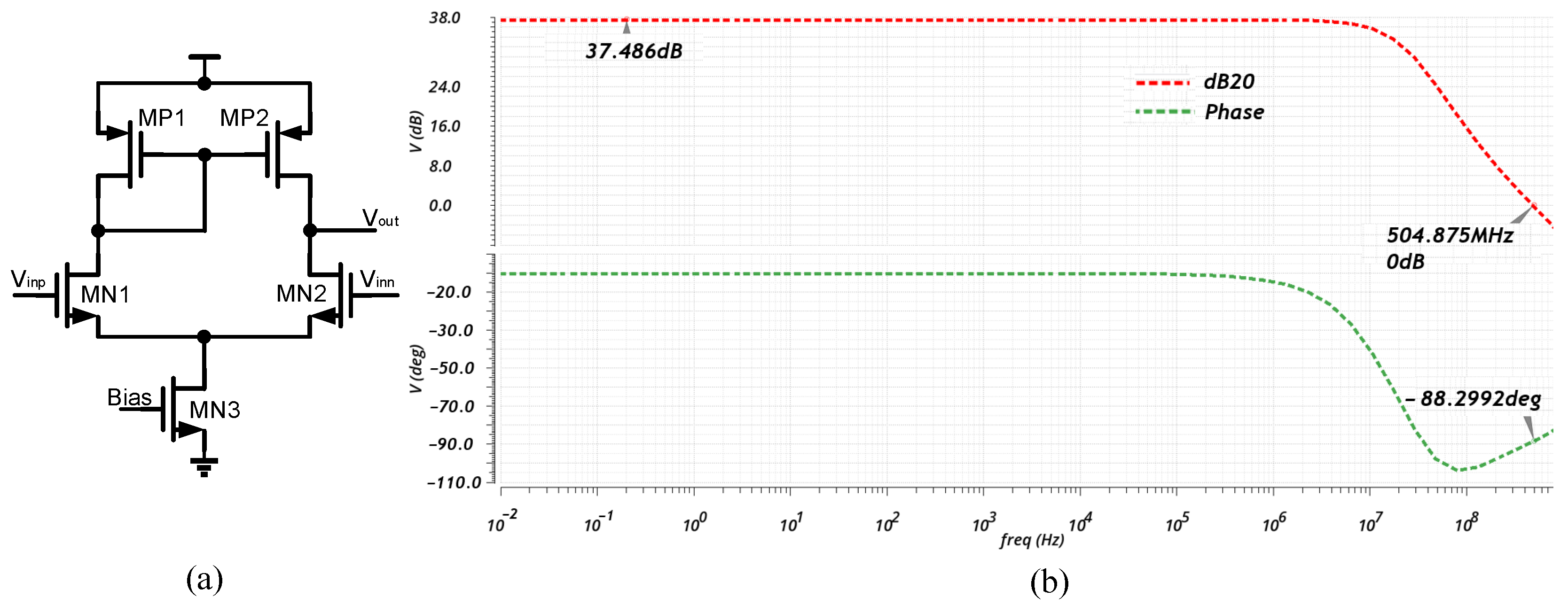
3.1. Front-End Circuit Design

In the readout circuit of the voltage-controlled oscillator (VCO)-type proposed in [7], the authors used a current-to-voltage converter (a MOS transistor) to convert current into voltage. This voltage then controls the output frequency of the VCO, and finally, digital circuits quantify the counter to achieve the final digital output.
A structural drawback of this setup is that while it is designed to quantify different column currents, the conversion from current to voltage results in changes in the voltage at point Y reflecting the variations in column currents. Changes in the voltage at point Y (point A in this paper) lead to modifications in the voltage difference across columns in the RRAM Crossbar, thus causing deviations in the column currents from their ideal values. To address this issue, this paper implements a negative feedback circuit formed by an operational amplifier and a current mirror, as shown in Figure 11a.
In the front-end circuit, the voltage at point A1 is clamped to V r e f . With this setup, as the changes in the LRS within the CIM array occur, the voltage at point A1 remains almost unchanged, as illustrated in Figure 11b. The voltage variations at point A1 in the circuit designed in the [7] are around 200 mV, whereas in the circuit designed in this paper, the voltage changes at point A1 are about 5 mV, which can be considered negligible. Hence, this structure enhances the linearity of the output column currents in the CIM array.
Within the circuit, the operational amplifier adopts a five-transistor architecture, as depicted in Figure 12a. Due to the requirement for the input to remain stable at 0.8 V, NMOS pair transistors are utilized for the input. The amplitude and phase frequency characteristic curves are shown in Figure 12b. The operational amplifier exhibits an approximate DC gain of 37.5 dB, with a phase margin of about 92°.
To achieve better current mirror matching in the circuit, the current mirror for the first array is divided into MN1,2, MN1,3, and MN1,4, with IB1, IB2, and IB3 each connected to one of the three CCOs in the CCO circuit. Furthermore, considering the near-mA scale current flowing through the columns of the CIM array, the width-to-length ratio of (MN1,2, MN1,3, MN1,4) is proportionally reduced to decrease power consumption in subsequent circuits.
The front-end circuit designed in this paper categorizes the four columns of the CIM array into four distinct weight classes: (MN1,2, MN1,3, MN1,4) represent weight 1, (MN2,2, MN2,3, MN2,4) have weight 2, (MN3,2, MN3,3, MN3,4) carry weight 4, and (MN4,2, MN4,3, MN4,4) are assigned weight 8. These weights are implemented at the physical layer, directly assigning weights to the columns, which effectively reduces the power consumption and area costs that would be incurred by digital logic operations for weight assignment. Table 1 provides the MOS transistor dimensions for the current mirrors shown in Figure 10.

3.2. Design of CCO

Traditional CCOs have limited suppression of fabrication process-sensitivity, which can lead to variations in the output frequency of the CCO, particularly in high-gain CCO designs. These frequency shifts can incur significant correction costs in subsequent circuit outputs. To address this challenge, this paper proposes a new low process-sensitive CCO structure, as demonstrated in Figure 13.
The IBn is the mirrored current from the current mirror in the front-end circuit flowing out of each delay unit. V D D denotes the power supply voltage, and V t h n 1 represents the threshold voltage of MN1. When the input V i n shifts from a low to a high level, MP1 and MP3 disconnect, MN3 conducts. Subsequently, the capacitor C i n t discharges through the current I C C O . Once the voltage on the bottom plate of C i n t drops to V t h n 1 , MN1 turns off, leading to a high inverter output and thus a low V o u t . Conversely, when V i n shifts from high to low, MP1 conducts and the current through MP1 recharges C i n t , resetting its voltage. With MP3 conducting and MN3 off, V o u t goes high. The output period of the CCO is given by the following equation:
T = N × [ C i n t ( V D D V t h n 1 ) I C C O + t r i s e + t f a l l ]
Here, N is the number of delay units (N = 3 in this design), t r i s e is the signal’s rising delay time, and t f a l l is the falling delay time. In practical circuits, t r i s e and t f a l l can be neglected compared to the first term within the parentheses in Equation (3). Thus, for simplification, the output waveform’s frequency is assumed to be a first-order function of I C C O .
The low process-sensitivity of this CCO structure is due to the complementary nature of changes in the value of C i n t with those of ( V D D V t h n 1 ) with respect to process variations. For instance, in an FF process corner, the value of C i n t and the threshold voltage V t h n 1 would decrease, while the value of ( V D D V t h n 1 ) would increase, thus reducing the changes in the product of C i n t ( V D D V t h n 1 ) . Table 2 provides the MOS transistor dimensions for the current mirrors shown in Figure 13. Moreover, the C i n t is equal to 1 pf.
Considering the approximate current range of 7.2 μA to 42 μA, the Monte Carlo simulation of CCO was operated with a current of 25 μA as I C C O , as depicted in Figure 14.

3.3. Digital Logic Circuit

The final output of the readout circuit under discussion is generated as a digital signal via a time-to-digital converter (TDC). Traditional TDC implementations typically use either counters or encoders. In time-delay-based ADC, encoder-based T/D conversion is common due to the circuit structure’s requirements. However, in this research, digital counters are the primary means for achieving T/D conversion [17].
The readout circuit does not impose high requirements on conversion speed. There are no stringent demands on the delay times of the digital modules. To fulfill objectives of low power consumption and reduced area, true single-phase clock (TSPC)-type flip-flops are employed within this structure. In TDCs utilizing digital counters, the output is expressed as:
F ( T ) = N C C O 2 N c l k × f c l k f C C O
Here, N c l k denotes the bit depth of the reference side counter, f c l k is the input frequency of the reference signal, N C C O represents the bit depth of the CCO output counter, and f C C O is the output waveform frequency of the CCO, with · indicating a floor function.
When the reference counter reaches a full count of N bits, it triggers the CCO side counter, with the count value of the CCO side counter representing the digital output at that moment. Consequently, the reference counter has fewer bits compared to the CCO counter, which has a greater number to prevent counting errors due to insufficient bit count, typically including a margin for redundancy.

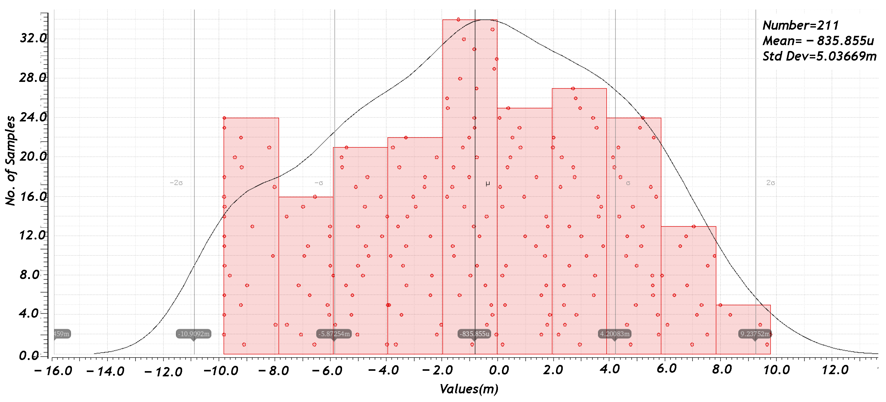
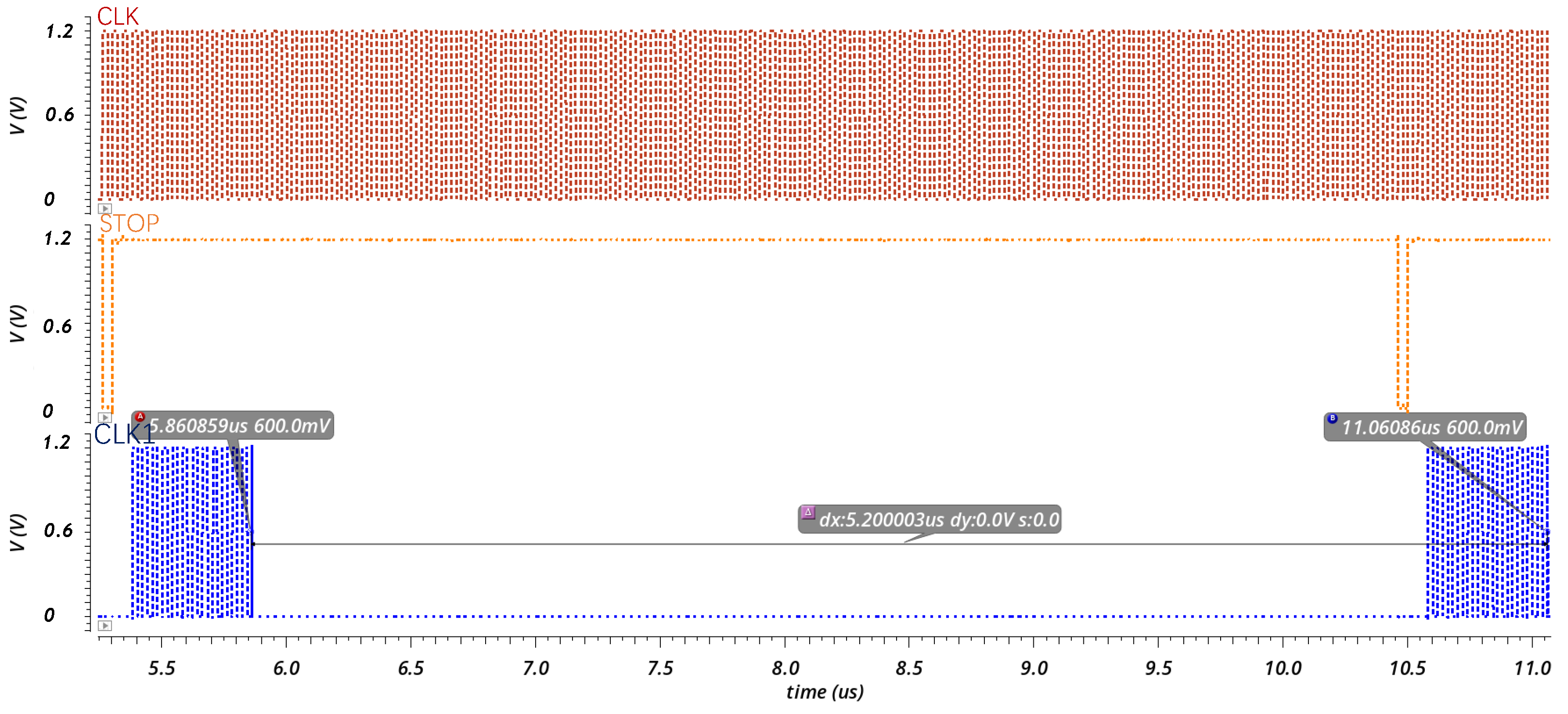
4. Simulation Results

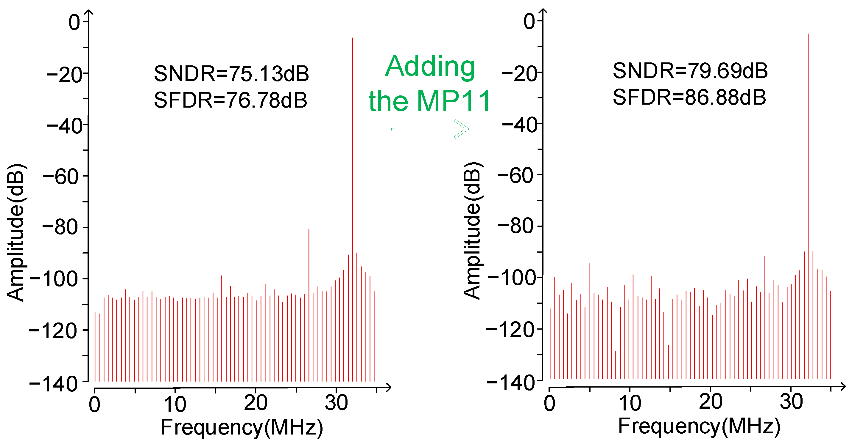
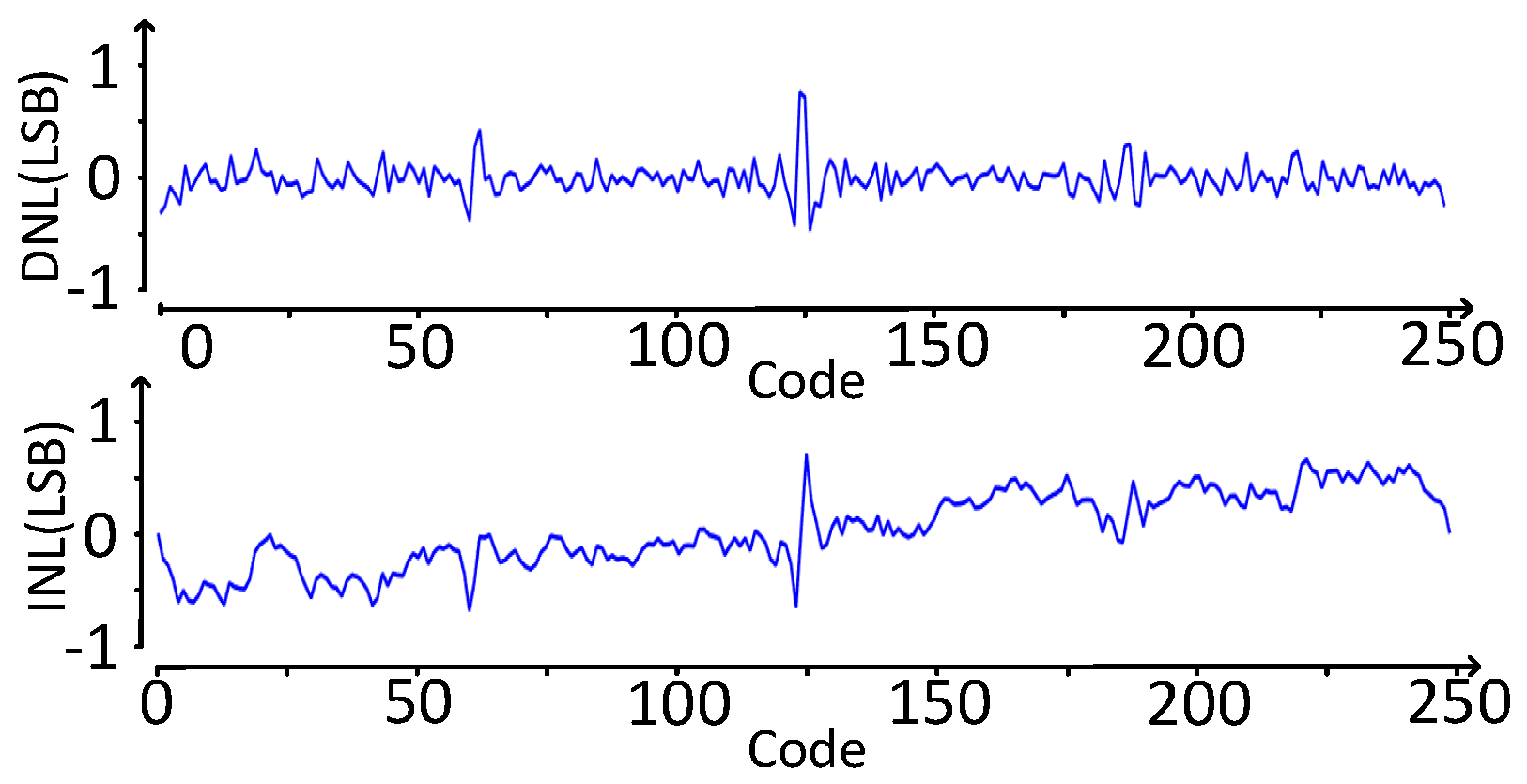
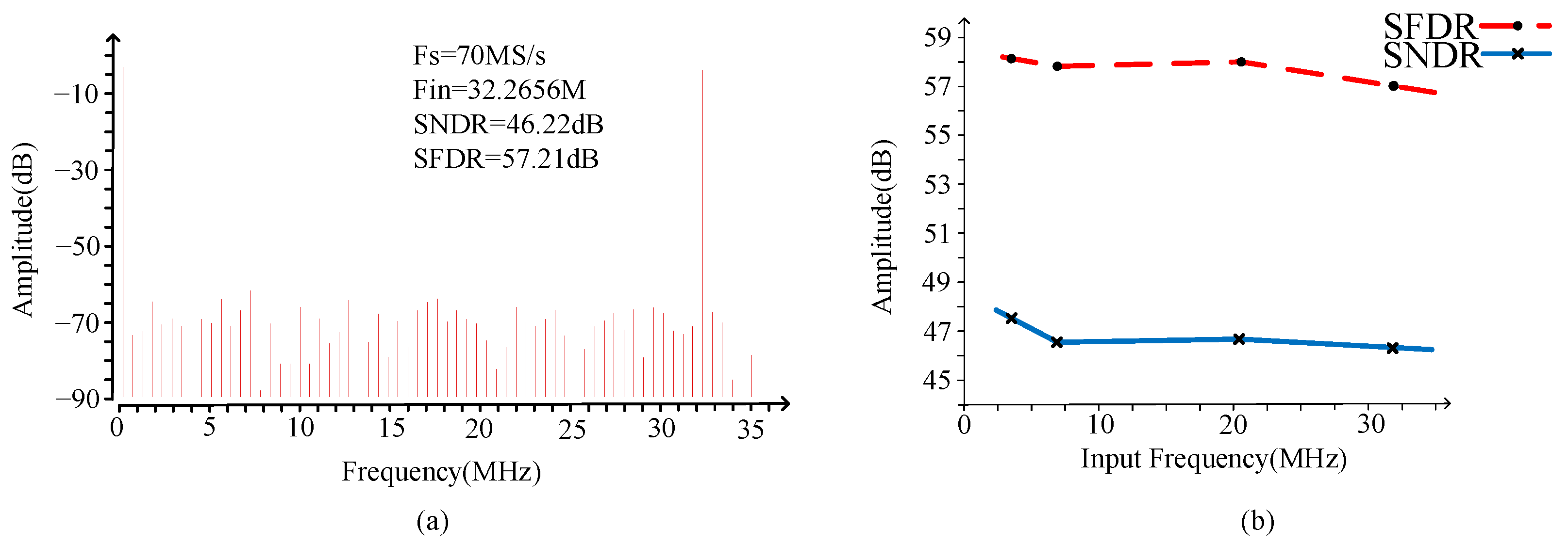
4.1. SAR ADC Readout Circuit Layout and Post-Simitation Results

The SAR ADC proposed in this study was designed utilizing SMIC 110 nm CMOS technology. By employing custom-designed capacitors, active devices were arranged beneath the CDAC array, utilizing metal layers M1 to M3 for routing. We present the simulation results conducted with a 1.2 V supply voltage in this subsection.
Figure 15a presents the performance metrics for the SAR ADC with a Nyquist-rate input. The results demonstrate SNDR of 46.22 dB, SFDR of 57.21 dB, and ENOB of 7.38 bits for the 70 MS/s sampling rate. Furthermore, Figure 15b displays the variation in SNDR and SFDR across different input frequencies. The observations reveal that the SFDR remains above 57 dB and the SNDR stays above 46 dB, with both metrics exhibiting a decrement of less than 2 dB as the input frequency escalates to the Nyquist rate.
The power dissipation observed for the system operating with a 1.2 V supply is measured at 553 μW. The distribution of power consumption across different components of the system is as follows: the DAC accounts for 7% of the total power dissipation; the comparator is responsible for 31%; the S/H circuit utilizes 2%; and the digital circuits collectively demand 60% of the power, as illustrated in Figure 16. Consequently, the achieved FoM performance is 47.26 fJ/Conv.
In this design, active devices are incorporated beneath custom-designed capacitors, employing M1 to M3 layers for routing. This arrangement culminates in a core area of 0.0025544 mm2 (49.6 μm × 51.5 μm), utilizing 110 nm CMOS technology, as depicted in Figure 17. A comparison with preceding SAR ADCs is presented in Table 3. It reveals that the current design achieves the minimum area footprint while delivering a competitive FoM at moderate operational speed. Consequently, this design is particularly suitable for CIM applications, demanding an ADC that is both space-efficient and energy-efficient.

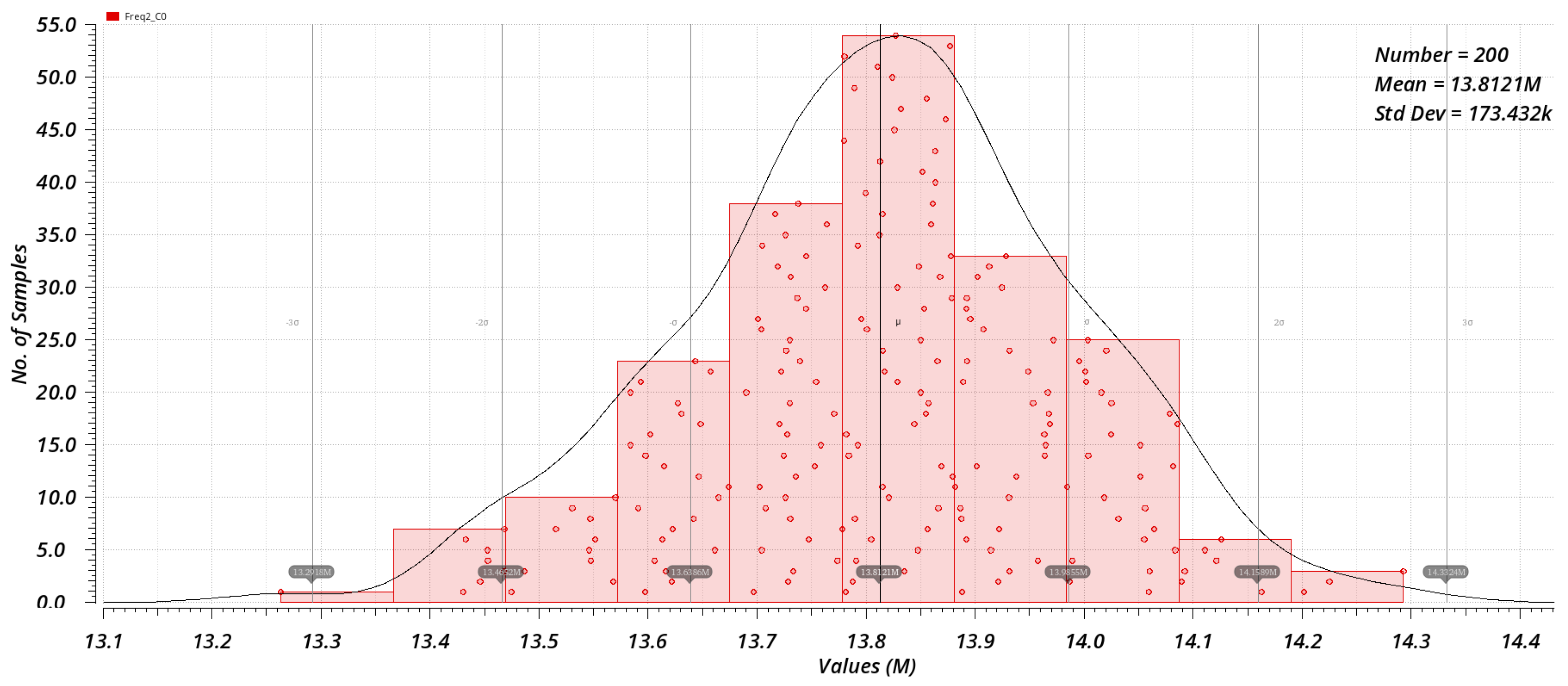
4.2. Simulation of Current-Controlled Oscillator-Type Readout Circuit

The 4 × 4 CIM array utilized in this paper assigns weightings of 1, 2, 4, and 8 to the first, second, third, and fourth columns, respectively. The RRAM employed has two states: an HRS (20 K Ω ) and an LRS (2 K Ω ). For each column, there are five types of current outputs associated with RRAM resistances of (2 K Ω , 2 K Ω , 2 K Ω , 2 K Ω ), (20 K Ω , 2 K Ω , 2 K Ω , 2 K Ω ), (20 K Ω , 20 K Ω , 2 K Ω , 2 K Ω ), (20 K Ω , 20 K Ω , 20 K Ω , 2 K Ω ), and (20 K Ω , 20 K Ω , 20 K Ω , 20 K Ω ). Given the distinct weights of the four columns in the CIM array, theoretically, this structure can yield 5 4 = 625 outcomes, denoted as N S = 625 .
With the reference CLK clock frequency set to 25 M, specific digital outputs post-quantification are derived based on Equation (4). Altering the high/low resistance state count for each RRAM column in the CIM yields digital outputs at the OUTPUT terminal of the digital logic module. When the RRAM in the 4 × 4 CIM array is entirely in the HRS, the OUTPUT yields 0001101; when entirely in the LRS, the OUTPUT yields 1111111. Statistical analysis performed using Python on the output results reveals a quantification of 95 outcomes within the range of 0001101 to 1111111, hence N D = 95 . These 95 outcomes are arranged in ascending order, as shown in Figure 18. The observed frequency discontinuities at both sides occur because the semiconductor device within the CCO (specifically, transistor MN1,1 in the current mirror of the front-end circuit) reaches its operational limits. At very low currents, the transistor enters the cut-off region, while at very high currents, it transitions to the linear region. Consequently, this leads to a non-ideal current–frequency relationship.
The delay L represents the interval between the OUTPUT terminal delivering an 8-bit result and the subsequent output of the next 8-bit result. With a reference CLK of 25 MHz, after 128 counts, the reference counter issues a STOP signal ceasing the counting at the CCO counter; concurrently, the parallel-to-serial state machine initiates conversion. After 12 CLK1 (with CLK1 frequency equal to CLK) cycles, the OUTPUT is complete. For efficiency, as OUTPUT begins, the CCO is reset, and the next counting cycle commences. The time from OUTPUT delivering a binary result until the next cycle’s binary output, as shown in Figure 19, sets the circuit delay L to 5.2 μs.
When varying numbers of HRS and LRS are configured in the CIM RRAM array, there is a significant variation in mirrored current from the front-end circuit, leading to a considerable change in power consumption for the front-end and CCO circuits. The average power consumption, P a v e r a g e , in this study is quantified by summing and then averaging the power consumption across all 625 scenarios:
P a v e r a g e = P 1 + P 2 + · · · P N N
Under a supply voltage of 1.2 V, transient simulations yield an estimation of power dissipation for the current-controlled oscillator-type readout circuit, as shown in Figure 20.
P1 is the power consumption of the front-end circuit, P2 is that of the CCO circuit, and P3 is the power consumption of the digital logic circuit. It is apparent from the figure that as the HRS/LRS change in the CIM array, resulting in current variations to the CCO, there is a corresponding fluctuation in power consumption due to the different frequencies of output. Calculating the average power consumption as per Equation (5), the average total power dissipation of the circuit structure is found to be 183.1 μW, of which the front-end circuit accounts for 94.7 μW, the CCO circuit for 86.8 μW, and the digital logic circuit for 1.6 μW. Their proportional contributions are illustrated in Figure 21.
The CCO-type readout circuit designed in this paper achieves a resolution of 95, delay of 5.2 μs, and power dissipation of 183.1 μW at a voltage of 1.2 V in TSMC 65 nm.
Table 4 provides a comparative analysis between the non-traditional readout circuit presented in this study and those reported in other research. This study adopts a method of distinct weighting for different CIM columns, providing a marked advantage in resolution relative to [7,22]. Compared to references [7,22], the circuit delay in this study is relatively larger. There are two main reasons for the extended time in our design. For the first, time and resolution are positively correlated. Taking [7] as an example, the paper designs a VCO-based readout circuit, and its results are only applicable to a single column in an RRAM array with the resolution of 32 levels. Our paper proposes a quantization approach for four columns of an RRAM array simultaneously (the weights for the four columns being 1, 2, 4, and 8, respectively) with the resolution of 95 levels. For the second, we scale down the current using current mirrors, which results in a frequency reduction in the CCO circuit. In turn, this leads to the growth of time. As power consumption metrics are not provided in [7,22], and the number of cycles is not specified, a comparison of power consumption is eschewed.

5. Conclusions

With the rapid evolution of AI technology and its expanding applications, increasingly sophisticated algorithms require superior computing power. The traditional von Neumann architecture is facing power limitations, causing substantial computational bottlenecks. To address this challenge, CIM architectures offer distinct advantages in processing CNN algorithms. However, the readout circuitry incurs significant power consumption and area overhead, often exceeding that of the compute array itself. This study investigates readout circuits within CIM using RRAM as the computational storage unit.
There are two prevalent designs: traditional ADC-type readout circuits and non-traditional types. Based on the former, a low-power, compact SAR ADC is designed as the core of the readout circuit for digital signal extraction. The prototype ADC occupies an active area of only 0.00255 mm2 (49.6 μm × 51.5 μm) and achieves an SNDR of 46.22 dB and an SFDR of 57.21 dB, with the Nyquist rate input at a sampling rate of 70 MS/s. The power consumption is 553 μW, resulting in a 47.26 fJ/Conv FOM at 1.2 V supply.
Nevertheless, the complex conversion process in traditional ADC types yields significant power and area costs, which can surpass the compute array. To overcome this drawback, the paper designs a CCO-type readout circuit. This CCO-type readout circuit design achieves a resolution of 95, delay of 5.2 μs, and power dissipation of 183.1 μW at a voltage of 1.2 V in TSMC 65 nm.

Author Contributions

X.X., under the supervisor’s guidance, designed two types of CIM readout circuits in both the schematic and layout phases and wrote the paper. A.W. proposed the topic, provided guidance and ideas for the design, and revised the paper. Y.S. assisted with the CLK generation and pad modules for the first readout circuit, as well as the CCO module for the second readout circuit. All authors have read and agreed to the published version of the manuscript.

Funding

This research received no external funding.

Data Availability Statement

Data is contained within the article.

Conflicts of Interest

The authors declare no conflicts of interest.

References

  1. Meng, F.H.; Lu, W.D. Compute-in-Memory Technologies for Deep Learning Acceleration. IEEE Nanotechnol. Mag. 2024, 18, 44–52. [Google Scholar] [CrossRef]
  2. Liu, Q.; Gao, B.; Yao, P.; Wu, D.; Chen, J.; Pang, Y.; Zhang, W.; Liao, Y.; Xue, C.X.; Chen, W.H.; et al. 33.2 A fully integrated analog ReRAM based 78.4 TOPS/W compute-in-memory chip with fully parallel MAC computing. In Proceedings of the 2020 IEEE International Solid-State Circuits Conference-(ISSCC), San Francisco, CA, USA, 16–20 February 2020; pp. 500–502. [Google Scholar]
  3. Lee, K.; Cheon, S.; Jo, J.; Choi, W.; Park, J. A charge-sharing based 8t sram in-memory computing for edge dnn acceleration. In Proceedings of the 2021 58th ACM/IEEE Design Automation Conference (DAC), San Francisco, CA, USA, 5–9 December 2021; pp. 739–744. [Google Scholar]
  4. Xiao, K.; Cui, X.; Qiao, X.; Song, J.; Luo, H.; Wang, X.; Wang, Y. A 28nm 32Kb SRAM computing-in-memory macro with hierarchical capacity attenuator and input sparsity-optimized ADC for 4b MAC operation. IEEE Trans. Circuits Syst. II Express Briefs 2023, 70, 1816–1820. [Google Scholar] [CrossRef]
  5. Chou, T.; Tang, W.; Botimer, J.; Zhang, Z. Cascade: Connecting rrams to extend analog dataflow in an end-to-end in-memory processing paradigm. In Proceedings of the 52nd Annual IEEE/ACM International Symposium on Microarchitecture, Columbus, OH, USA, 12–16 October 2019; pp. 114–125. [Google Scholar]
  6. Liu, H.; Qian, Z.; Wu, W.; Ren, H.; Liu, Z.; Ni, L. AFPR-CIM: An Analog-Domain Floating-Point RRAM-based Compute-In-Memory Architecture with Dynamic Range Adaptive FP-ADC. arXiv 2024, arXiv:2402.13798. [Google Scholar]
  7. Mayahinia, M.; Singh, A.; Bengel, C.; Wiefels, S.; Lebdeh, M.A.; Menzel, S.; Wouters, D.J.; Gebregiorgis, A.; Bishnoi, R.; Joshi, R.; et al. A voltage-controlled, oscillation-based adc design for computation-in-memory architectures using emerging rerams. ACM J. Emerg. Technol. Comput. Syst. 2022, 18, 1–25. [Google Scholar] [CrossRef]
  8. Singh, A.; Lebdeh, M.A.; Gebregiorgis, A.; Bishnoi, R.; Joshi, R.V.; Hamdioui, S. Srif: Scalable and reliable integrate and fire circuit adc for memristor-based cim architectures. IEEE Trans. Circuits Syst. Regul. Pap. 2021, 68, 1917–1930. [Google Scholar] [CrossRef]
  9. Harpe, P.; Zhou, C.; Wang, X.; Dolmans, G.; de Groot, H. A 30fJ/conversion-step 8b 0-to-10MS/s asynchronous SAR ADC in 90 nm CMOS. In Proceedings of the 2010 IEEE International Solid-State Circuits Conference-(ISSCC), San Francisco, CA, USA, 7–11 February 2010; pp. 388–389. [Google Scholar]
  10. Chen, H.; He, L.; Deng, H.; Yin, Y.; Lin, F. A high-performance bootstrap switch for low voltage switched-capacitor circuits. In Proceedings of the 2014 IEEE International Symposium on Radio-Frequency Integration Technology, Hefei, China, 27–30 August 2014; pp. 1–3. [Google Scholar]
  11. Xu, X.; Shui, Y.; Wang, A. A 0.0025 mm 2 8-bit 70MS/s SAR ADC with a Linearity-Improved Bootstrapped Switch for Computation in Memory. In Proceedings of the 2023 8th International Conference on Integrated Circuits and Microsystems (ICICM), Nanjing, China, 20–23 October 2023; pp. 412–416. [Google Scholar]
  12. Khorami, A.; Dastjerdi, M.B.; Ahmadi, A.F. A low-power high-speed comparator for analog to digital converters. In Proceedings of the 2016 IEEE International Symposium on Circuits and Systems (ISCAS), Montreal, QC, Canada, 22–25 May 2016; pp. 2010–2013. [Google Scholar]
  13. Ginsburg, B.P.; Chandrakasan, A.P. An energy-efficient charge recycling approach for a SAR converter with capacitive DAC. In Proceedings of the 2005 IEEE International Symposium on Circuits and Systems, Kobe, Japan, 23–26 May 2005; pp. 184–187. [Google Scholar]
  14. Wang, A.; Shi, C.J.R. A 10-bit 50-MS/s SAR ADC with 1 fJ/conversion in 14 nm SOI FinFET CMOS. Integration 2018, 62, 246–257. [Google Scholar] [CrossRef]
  15. Jiang, Z.; Wong, H.S.P. Stanford University resistive-switching random access memory (RRAM) Verilog-A model. nanoHUB 2014. [Google Scholar]
  16. Shui, Y.; Wang, A. A 14.17 pJ·K2 FoM CMOS Temperature Sensor with 173 μm2 Sensing Core for Remote Sensing in 65 nm CMOS. IEEE Sens. J. 2023, 23, 27059–27067. [Google Scholar] [CrossRef]
  17. Yoon, Y.G.; Park, S.H.; Cho, S. A time-based noise shaping analog-to-digital converter using a gated-ring oscillator. In Proceedings of the 2011 IEEE MTT-S International Microwave Workshop Series on Intelligent Radio for Future Personal Terminals, Daejeon, Republic of Korea, 24–25 August 2011; pp. 1–4. [Google Scholar]
  18. Liu, S.; Rabuske, T.; Paramesh, J.; Pileggi, L.; Fernandes, J. Analysis and background self-calibration of comparator offset in loop-unrolled SAR ADCs. IEEE Trans. Circuits Syst. Regul. Pap. 2017, 65, 458–470. [Google Scholar] [CrossRef]
  19. Tang, F.; Ma, Q.; Shu, Z.; Zheng, Y.; Bermak, A. A 28 nm cmos 10 bit 100 ms/s asynchronous sar adc with low-power switching procedure and timing-protection scheme. Electronics 2021, 10, 2856. [Google Scholar] [CrossRef]
  20. Zhao, J.; Huang, Z.; Hou, X. A 10-bit 50-ms/s asynchronous sar adc in 65nm cmos. In Proceedings of the 2022 IEEE 14th International Conference on Advanced Infocomm Technology (ICAIT), Chongqing, China, 8–11 July 2022; pp. 225–229. [Google Scholar]
  21. Huang, Y.; Luo, C.; Guo, G. A cryogenic 8-bit 32 ms/s sar adc operating down to 4.2 k. Electronics 2023, 12, 1420. [Google Scholar] [CrossRef]
  22. Liu, C.; Yan, B.; Yang, C.; Song, L.; Li, Z.; Liu, B.; Chen, Y.; Li, H.; Wu, Q.; Jiang, H. A spiking neuromorphic design with resistive crossbar. In Proceedings of the 52nd Annual Design Automation Conference, San Francisco, CA, USA, 7–11 June 2015; pp. 1–6. [Google Scholar]
Figure 1. Block and timing diagrams of the proposed SAR ADC.
Electronics 13 02478 g001
Figure 2. The bootstrapped switch structure.
Electronics 13 02478 g002
Figure 3. Bootstrapped switch dynamic performance.
Electronics 13 02478 g003
Figure 4. (a) Traditional two-stage dynamic comparator and (b) transconductance-enhanced two-stage dynamic comparator.
Electronics 13 02478 g004
Figure 5. Monte Carlo simulation of the comparator offset voltage.
Electronics 13 02478 g005
Figure 6. Comparison of V o u t waveforms from two comparators.
Electronics 13 02478 g006
Figure 7. 3D model of capacitance with shielding in one direction [11].
Electronics 13 02478 g007
Figure 8. DNL and INL simulation results.
Electronics 13 02478 g008
Figure 9. 4 × 4 CIM array.
Electronics 13 02478 g009
Figure 10. CCO-type readout circuit structure.
Electronics 13 02478 g010
Figure 11. (a) The front-end circuit and (b) change of point A1 with the number of LRS ( V r e f = 0.8 V).
Electronics 13 02478 g011
Figure 12. (a) The operational amplifier structure and (b) its amplitude frequency response and phase response.
Electronics 13 02478 g012
Figure 13. Low process-sensitive CCO circuit.
Electronics 13 02478 g013
Figure 14. Monte Carlo simulation of the CCO.
Electronics 13 02478 g014
Figure 15. (a) FFT spectrum at 70 MS/s and (b) dynamic performance versus different input frequencies [11].
Electronics 13 02478 g015
Figure 16. Power dissipation I.
Electronics 13 02478 g016
Figure 17. The layout of the proposed ADC [11].
Electronics 13 02478 g017
Figure 18. Distribution of 95 outcomes.
Electronics 13 02478 g018
Figure 19. Time delay.
Electronics 13 02478 g019
Figure 20. Power distribution in 625 cases.
Electronics 13 02478 g020
Figure 21. Power dissipation II.
Electronics 13 02478 g021
Table 1. MOS transistors size configuration of current mirror in front-end circuit.
MOSMN1,1–MN4,1MN1,2–MN1,4MN2,2–MN2,4MN3,2–MN3,4MN4,2–MN4,4
W/L20 μ /600n120n/600n240n/600n480n/600n960n/600n
Table 2. MOS transistors size configuration of current mirror in front-end circuit.
MOSMN1MN2MN3MP1MP2MP3
W/L600n/200n120n/60n120n/60n3 μ /60n1 μ /200n240n/60n
Table 3. Comparison with previous works I.
[18] *[19] *[20] +[21] +This Work +
Technology (nm)1302865180110
Active Area (mm2)0.0480.0260.1050.2530.00255
Resolution (bits)8101088
Supply (V)1.20.91.21.81.2
Sampling Rate (MS/s)150100503270
SNDR (dB)42.951.5452.0947.746.2
ENOB (bits)6.838.278.367.637.4
Power (W)640 μ 1.1 m2.79 m2.4 m553 μ
FOM (fJ/Conv.-step)37.535.616937847.26
*: testing results, and +: post-layout simulation results.
Table 4. Comparison with previous works II.
[22][7]This Work +
Technology (nm)-2865
Time delay (s)400n10n5.2 μ
Resolution (level)203295
+: pre-simulation results.
Disclaimer/Publisher’s Note: The statements, opinions and data contained in all publications are solely those of the individual author(s) and contributor(s) and not of MDPI and/or the editor(s). MDPI and/or the editor(s) disclaim responsibility for any injury to people or property resulting from any ideas, methods, instructions or products referred to in the content.

