Article

Baseline Calibration Scheme Embedded in Single-Slope ADC for Gas Sensor Applications

Department of Semiconductor Engineering, Seoul National University of Science and Technology, Seoul 01811, Republic of Korea
*
Author to whom correspondence should be addressed.
Electronics 2024, 13(7), 1252; https://doi.org/10.3390/electronics13071252
Submission received: 4 March 2024 / Revised: 21 March 2024 / Accepted: 25 March 2024 / Published: 28 March 2024
(This article belongs to the Special Issue Analog and Mixed-Signal Circuit Designs and Their Applications)

Abstract

:
This paper introduces a single-slope analog-to-digital converter (SS ADC) with an embedded digital baseline calibration scheme designed to improve the accuracy and reliability of gas sensor measurements. The proposed SS ADC effectively leverages an up/down counter mechanism to ensure stable signal extraction from gas sensors, despite variations in the baseline distribution. The proposed SS ADC initiates with a down counting operation to capture the initial output value of the gas sensor, which, after A/D conversion, is stored as a reference point for future readings. Subsequent gas sensor output values are derived by performing an up counting operation from this baseline reference. This approach allows for real-time correction of the baseline during the SS A/D conversion process, obviating the need for complex post-processing and baseline correction algorithms. The proposed SS ADC with the baseline calibration scheme was designed using a 0.18 μm standard CMOS process to confirm its feasibility. It demonstrated a signal-to-noise and distortion ratio (SNDR) of 57.56 dB and a spurious-free dynamic range (SFDR) of 59.02 dB, resulting in an effective number of bits (ENOB) of 9.27 bits in the post-simulation level. The proposed SS ADC has a total power consumption of 1.649 mW. This work offers an efficient solution to the baseline distribution problem in gas sensors, facilitating more reliable and accurate gas detection systems.

1. Introduction

Recently, the marketability of gas sensor systems is rapidly expanding, driven by increasing demands across a broad spectrum of industries including environmental monitoring, industrial safety, healthcare, automotive, and smart buildings [1,2,3]. The critical role of gas sensors in identifying hazardous gases, tracking air quality, and safeguarding workplace safety underscores the pressing need for ongoing technological advancements in this domain [4]. Among the various types of gas sensors, semiconductor sensors stand out due to their distinct characteristics and advantages [5,6,7,8]. Semiconductor gas sensors, often based on metal oxide semiconductors, offer high sensitivity to a wide range of gases at relatively low costs [9,10]. These sensors operate on the principle that the resistance of the semiconductor material changes in the presence of target gases, enabling the detection of gas concentrations. The advantages of semiconductor sensors include their compact size, low power consumption, and ability to operate at room temperature, making them ideal for portable and fixed monitoring systems [11].
However, the baseline dispersion of gas sensors poses a significant challenge, including semiconductor types [12,13,14]. Baseline dispersion refers to the variability or drift in the sensor’s baseline signal over time, which can occur due to changes in ambient conditions, the aging of the sensor, or exposure to background gases. This variability complicates the extraction of accurate and reliable signals from gas sensors, as it can mask the presence of target gases or lead to false readings. From the perspective of readout systems designed to extract signals from gas sensors, addressing baseline dispersion is crucial for maintaining the precision and accuracy of gas measurements. That is, the difficulty lies in distinguishing between changes in sensor signals caused by target gas concentrations and those resulting from baseline dispersion. Addressing the issue of baseline dispersion in gas sensors is a critical challenge that can be mitigated through sophisticated post-digital processing techniques [15,16]. However, it is important to acknowledge that these solutions necessitate the use of complex processing algorithms and additional computation resources. This requirement may, in turn, impact the technological competitiveness of gas sensor systems, because the need for resource-intensive algorithms could potentially slow down the processing time or increase the cost of the sensor systems.
Meanwhile, by focusing on the readout integrated circuit (ROIC), another crucial component in the gas sensor system, we can uncover potential solutions to significantly alleviate the physical limitations inherent in the gas sensor itself [12,17,18]. Specifically, when it comes to the baseline dispersion problem of gas sensors, by integrating advanced correction techniques and algorithms within the ROIC, it is possible to dynamically adjust and compensate for the baseline in real time, enhancing the sensor’s accuracy and reliability. This approach not only streamlines the post-calibration process but also mitigates the need for extensive post-processing, presenting a more efficient and effective strategy for overcoming challenges in gas sensor technology.
In this paper, we present an efficient baseline digital calibration scheme embedded in a single-slope (SS) ADC [12,19] for gas sensor readout. The proposed SS ADC enables stable gas signal extraction from gas sensors, unaffected by baseline distribution variations. This method involves initially down counting the output value of the gas sensor at the start of the measurement. After the analog-to-digital (A/D) conversion, this initial value is stored and serves as a reference point for subsequent measurements. The output value of the gas sensor is then extracted by up counting from this stored value for each new measurement. Through this SS A/D conversion process, the baseline value of the gas sensor is effectively corrected in real time. This approach circumvents the need for complex post-processing and baseline correction algorithms, allowing for the precise extraction of changes in the gas sensor’s output signal without the requirement of manually removing or adjusting the baseline drift.
The remainder of this paper is organized as follows: Section 2 examines the characteristics of the baseline variation. Section 3 describes the proposed SS ADC with the baseline digital calibration scheme. The simulation results of the proposed scheme are discussed in Section 4. Finally, the conclusions are presented in Section 5.

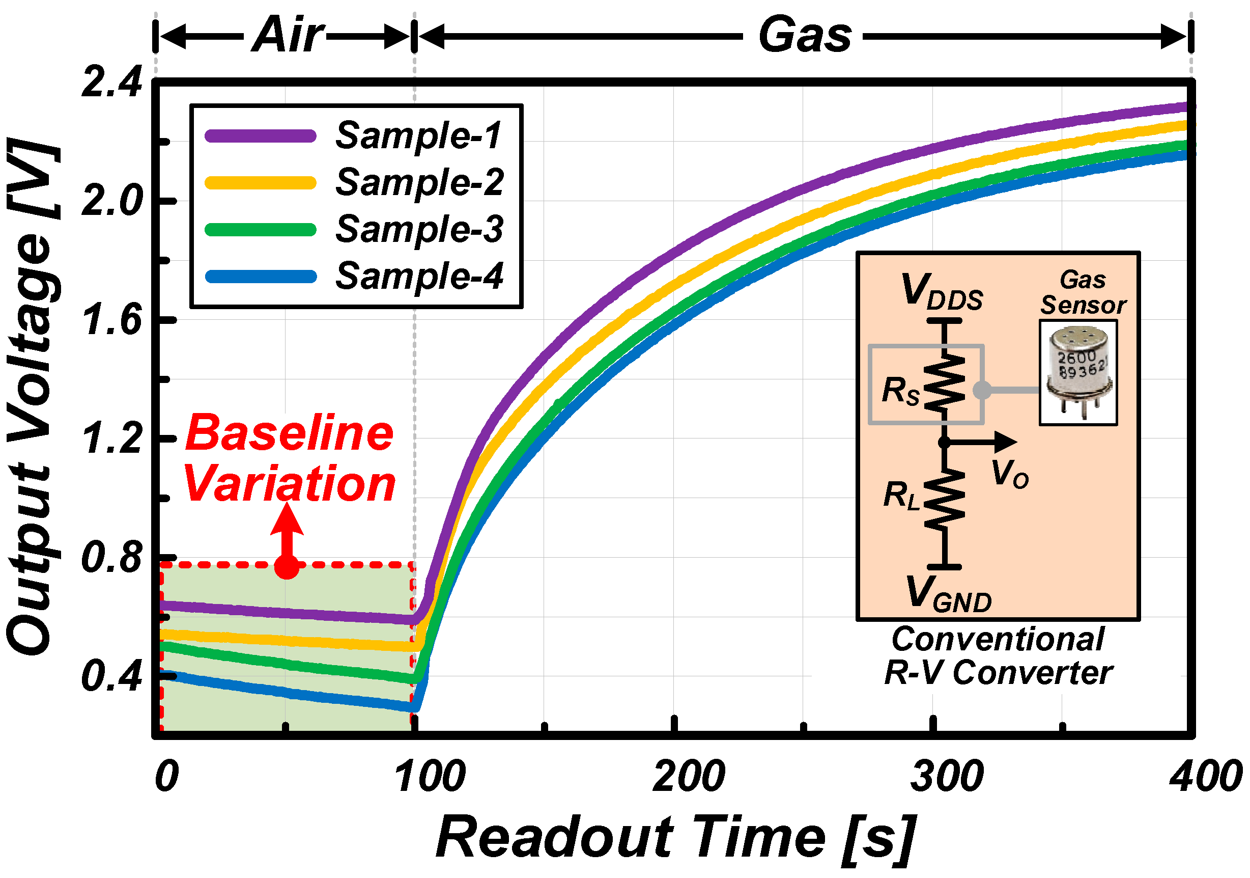
2. Characteristics of Baseline Variation

Figure 1 shows the baseline distribution across different gas sensor samples. The gas sensor outputs encapsulated by the red box show the output results stabilizing after the introduction of air, representing a baseline variation situation. Gas sensors [20,21] are characterized by their resistance change (RS) in response to gas concentrations, a fundamental property that allows for the detection of gas presence and concentration levels. To convert this resistance change into a measurable output, a load resistance (RL) is utilized for resistance-to-voltage (R-V) conversion, using a supply voltage (VDDS) to transform the gas concentration into a voltage signal (VO) [22]. However, a significant challenge arises due to the intrinsic material characteristic variability among gas sensors. This variability leads to differing baseline resistances, resulting in disparate output values (VO) for the same gas concentration across sensors. Such baseline variation complicates the accurate extraction of gas concentration information, as a standard R-V conversion circuit may not account for these discrepancies effectively. In light of this, accurate gas concentration determination becomes challenging with conventional R-V conversion circuits alone, necessitating additional post-processing digital signal processing (DSP) after the initial signal extraction. This requirement for complex DSP not only increases the processing burden but also impacts the technological competitiveness of gas sensor systems by adding layers of complexity and potential points of failure. To address the challenges of accuracy and reliability in gas concentration measurements, efforts to develop embedded baseline calibration methods within readout circuit designs are necessary. By enabling gas sensor readout circuits to adapt to baseline variability during signal extraction, the dependency on post-processing DSP can be reduced, thereby improving the performance and competitiveness of gas sensor systems. Based on these motivations, this paper introduces a simple yet powerful baseline calibration technique embedded within the readout ADC design, along with verification results demonstrating its effectiveness.

3. Proposed SS ADC with Baseline Calibration Scheme

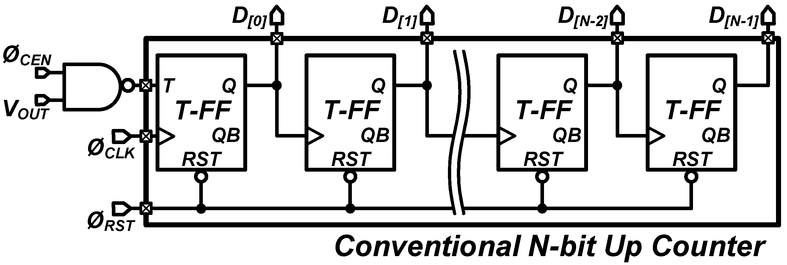
3.1. Typical SS ADC for Gas Sensor Readout

Figure 2a provides a simplified block diagram of a conventional single-slope analog-to-digital converter (SS ADC), which is particularly advantageous for integration with gas sensors due to its simplicity and effective linear performance [12,23]. It is composed of a comparator that contrasts the input signal with a reference signal, a ramp generator responsible for producing the reference signal for A/D conversion, an N-bit counter that counts the digital code until the comparator’s output trigger, and the digital control logic that manages the overall A/D conversion process. Figure 2b illustrates an operational timing diagram of the conventional SS ADC. When the ØIN is switched on, the input voltage (VIN) is sampled onto the sampling capacitor (CSH) and subsequently directed to the negative node of the comparator (VINN). With the activation of the ØCEN, the ramp generator begins to advance the A/D reference voltage (ΔVRAMP), which propels the positive node (VINP). The counter begins to increment the digital code step by step as soon as the ramp voltage (VINP) starts to rise. It continues this process until VINP rises below the sampled input voltage at VINN. At this moment, the comparator generates an output signal (VOUT) which halts the counter’s progression. The digital code value registered at this instant is then used to represent the A/D conversion result for the input voltage (VIN).
The SS ADC architecture is notably less complex than other ADC architectures, which is especially beneficial when employed in gas sensor readout ADCs. This simplicity ensures that the slow response times characteristic of gas sensors do not adversely affect the ADC’s performance, thus maintaining real-time monitoring capabilities. Additionally, the single-slope configuration reduces the overall complexity of the ADC design, potentially lowering manufacturing costs and facilitating scalability within extensive sensor networks. The SS ADC’s compatibility with the gas sensors’ slow dynamics makes it an ideal choice for accurate and reliable gas detection required in various applications.
Figure 3 shows a simplified conventional N-bit binary up counter, which is typically used in SS ADCs [24]. This counter is composed of toggle flip-flops (T-FFs), with the output Q of each flip-flop representing a digital output bit of the counter. The first T-FF in the sequence is known as the least significant bit (LSB) T-FF, which receives the clock pulse (ØCLK) and is the first to toggle. Each T-FF in the chain represents an increasing bit significance, forming the binary count as the circuit operates. When the flip-flop toggles, it signifies a binary ‘1’ in that bit position, and when it is reset, it represents a binary ‘0’. The counting sequence is initiated by the ØCLK that is applied to the LSB T-FF. Subsequent flip-flops receive the clock input from the preceding flip-flop’s output (Q), thus creating a cascading count effect throughout the bit chain. The Q of each T-FF indicates an individual bit of the final binary count, with the collection of these outputs (D[0] to D[N−1]) representing the digital count corresponding to the analog input signal. The asynchronous reset input (ØRST) allows for the entire counter to be reset instantaneously. When a ‘Low’ is applied to ØRST, all Qs of the T-FFs are driven to ‘0’, effectively clearing the counter and setting it to its initial state. The counter’s operation is controlled by a combined enable signal derived from the NAND gate that processes the counter enable signal (ØCEN) and the comparator’s output signal (VOUT). This enable signal allows the counter to proceed with counting only when ØCEN is active, and VOUT is in a state indicating that the comparator has not yet detected the VRAMP reaching the VIN. The counter stops counting when the comparator outputs the VOUT, indicating that the VRAMP has reached the VIN, thereby capturing the count at that precise moment as the digital equivalent of the analog input signal. This design ensures that the SS ADC can accurately and efficiently convert analog inputs into digital representations by counting in a binary sequence corresponding to the duration for which the reference voltage exceeds the input signal.

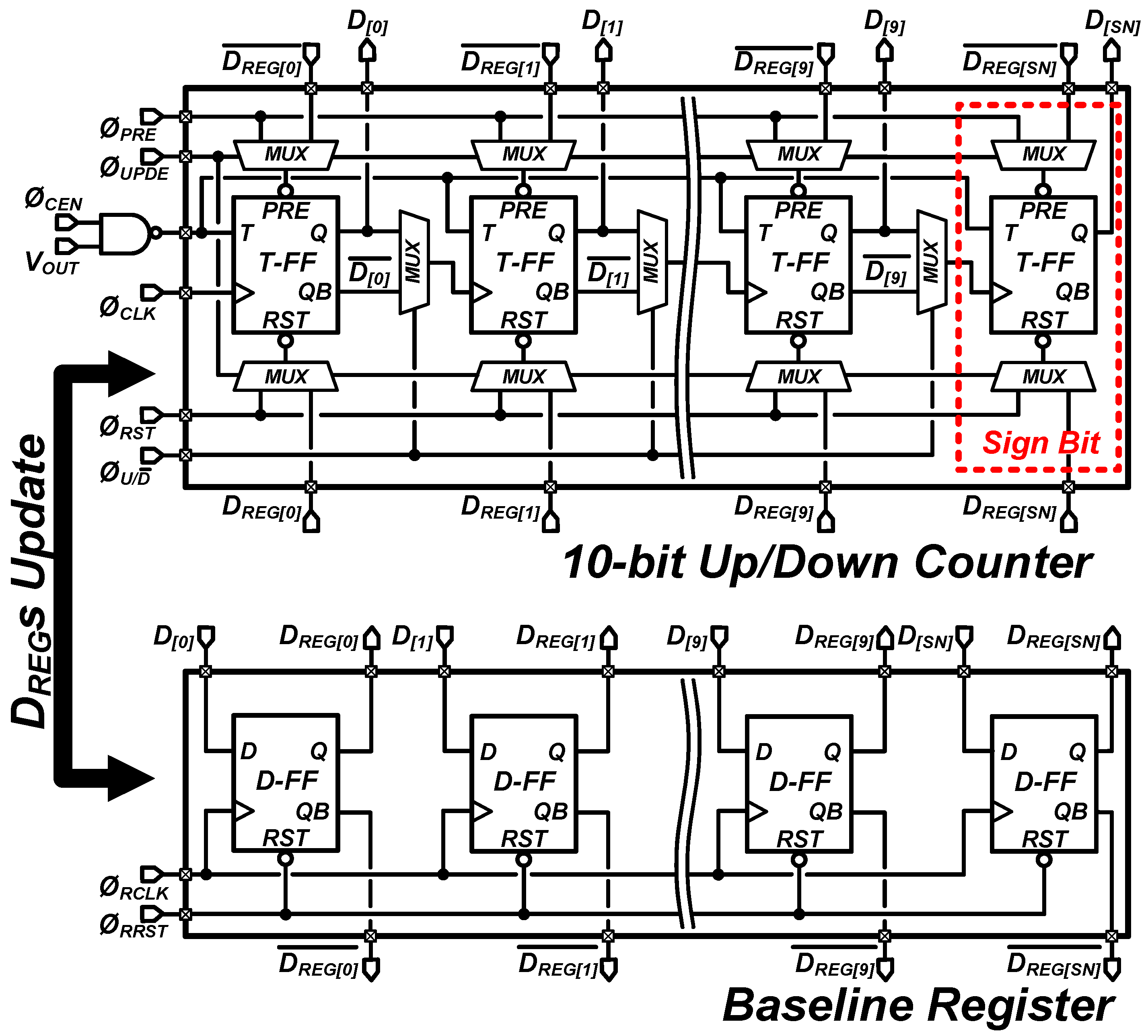
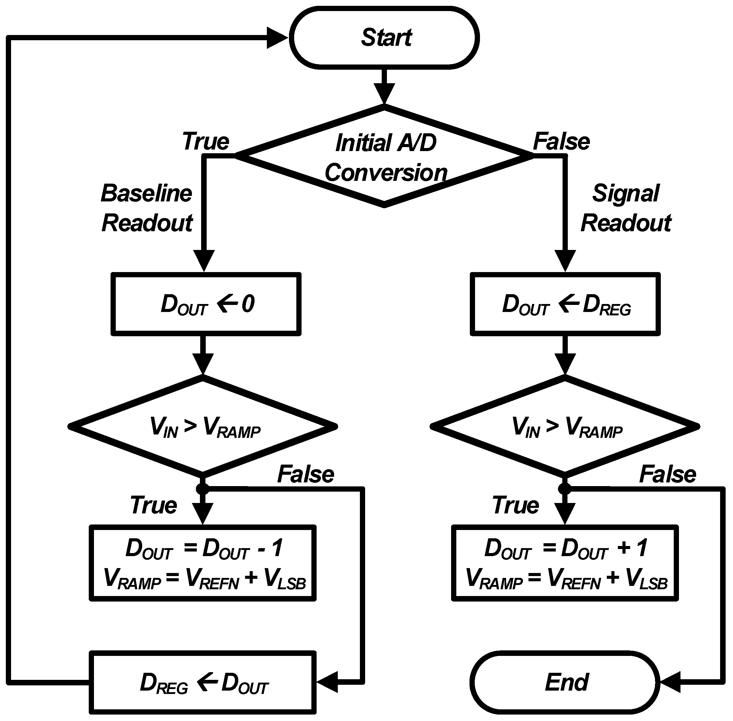
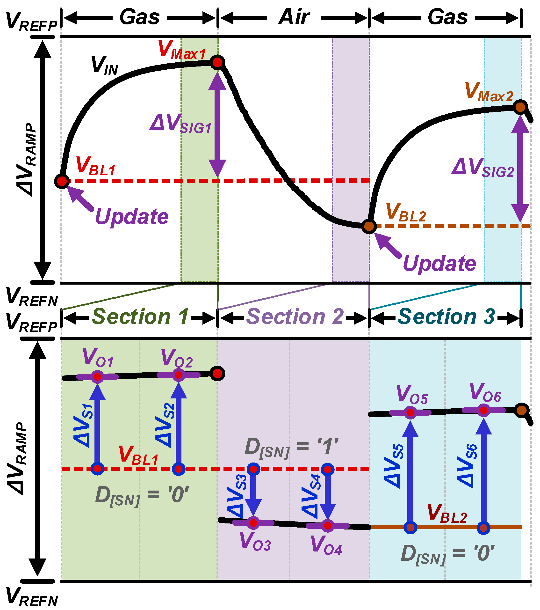
3.2. Proposed Baseline Calibration Scheme

The slow response characteristics of gas sensors are important factors to consider when implementing an effective baseline calibration scheme. To compensate for baseline variations that may vary with environmental variables such as temperature, humidity, etc., it is suitable to digitally store baseline information. Effectively, if the change in gas sensor output relative to this stored baseline information can be quantified through A/D conversion, it would facilitate the implementation of the baseline calibration scheme.
Figure 4 shows a simplified schematic of the proposed SS A/D counter with an embedded baseline calibration scheme specifically designed to address the slow response characteristics of gas sensors. The proposed counter is based on a 10-bit up/down counter structure [25] to achieve a 10-bit A/D resolution, with an added most significant (MSB) bit serving as a sign bit (D[SN)). An additional 11-bit baseline register is incorporated to update the baseline value of the gas sensor, with its input connected to the digital output bus D[SN:0] and its output linked to the multiplexers (MUXs) located at the counter’s reset and preset inputs. The counter’s operation range, defined by D[N−1]:D[0], spans from −(2(N−1) − 1) to (2(N−1) − 1), allowing for both positive and negative decimal values with the MSB indicating the sign. The counter can select between the Q and QB outputs from each stage through the MUX switches, controlled by the external signal ØU/D. When ØU/D is ‘HIGH’, Q is selected for up counting, and when ØU/D is ‘LOW’, QB is chosen for down counting. Moreover, when ØUPDE is ‘HIGH’, the outputs of the register DREG[SN:0] and D R E G [ S N : 0 ] ¯ are applied to the T-FF’s reset (RST) and preset (PRE), respectively. If DREG[N] is ‘LOW’, the T-FF’s RST is activated, setting the corresponding digital output bit D[N]’s Q to 0. Conversely, if DREG[N] is ‘HIGH’, the T-FF’s PRE is activated, setting D[N]’s Q to 1. This operation mechanism allows for dynamic updating of the baseline value in response to environmental changes, ensuring accurate gas sensor readings.
Figure 5 provides operational examples of the proposed counter structure with the baseline calibration scheme, illustrating cases when the sign bit (D[SN]) is set to ‘0’ and ‘1’. The operation procedure is divided into two phases: the baseline readout phase for establishing the reference point and the signal readout phase for measuring the gas concentration. During the baseline readout phase, the initial value of the gas sensor, which serves as the baseline, is captured to commence SS A/D conversion. At this stage, with the ØU/D signal set to low, the proposed counter conducts down counting until the comparator is triggered, obtaining the baseline value (−DBL). This value is then stored in the baseline register as DREG when triggered by ØRCLK. In the signal readout phase, the −DBL value is updated as the initial value of the proposed counter each time ØUPDE is triggered. With ØU/D set to high, the counter performs up counting from the −DBL, effectively extracting the output signal of the gas sensor. Since the counter starts from −DBL, the gas sensor’s baseline value is compensated for during the conversion process, and the SS A/D conversion result is represented as DSIG − DBL. Figure 5a represents the case where DSIG − DBL ≥ 0, indicating that the absolute value of DSIG is greater than the initial DBL. Here, the sign bit D[SN] is set to ‘LOW’, and the final output code has a positive sign with a magnitude of DSIG − DBL. Conversely, Figure 5b depicts the case where DSIG − DBL < 0, meaning the absolute value of DSIG is less than DBL. In this instance, D[SN] is set to ‘HIGH’, and the final output code carries a negative sign with a magnitude of DSIG − DBL. Through this process, by extracting a signal that correlates with the initial baseline code of the gas sensor, the output DSIG effectively performs baseline digital calibration without the need for additional post-processing digital calibration. This scheme ensures that the gas sensor’s output is accurately represented in relation to its baseline, thus facilitating a more streamlined and efficient signal processing operation.
Figure 6 shows the overall process of the proposed baseline calibration algorithm embedded in the SS ADC. The operational algorithm is bifurcated into two distinct cases: baseline readout and signal readout. For the initial A/D conversion, the algorithm carries out the A/D conversion for the baseline. It commences by resetting DOUT to zero. If VIN is greater than VRAMP, the algorithm executes the down counting operation by decrementing DOUT by one LSB (DOUT = DOUT − 1). Concurrently, VRAMP is incremented by one LSB in a process that is synchronized with the counter clock, repeating this sequence until VIN becomes less than VRAMP. At this moment, DOUT is stored in DREG, which is then utilized as the baseline (−DBL). If the operation does not consist of the initial A/D conversion, DOUT is set to the stored −DBL value. When VIN exceeds VRAMP, DOUT undergoes an up counting operation, increasing by one LSB. Once VIN becomes less than VRAMP, the current value of DOUT represents the actual change in the gas sensor’s signal and concludes the A/D conversion process. In the proposed baseline calibration algorithm, the down counting and up counting mechanisms are key points for dynamically adjusting the A/D conversion process based on VIN, ensuring that the ADC output reflects real-time changes in gas concentration.
Figure 7 illustrates the effectiveness of the proposed baseline calibration scheme for gas sensor signal extraction when faced with baseline voltage variations due to environmental changes or sensor activation. This demonstrates how the proposed scheme accommodates VBL and extracts the actual change in the gas sensor signal, ΔVSIG. Initially, before gas exposure, the SS ADC converts VBL into DBL, which is stored in the baseline register. This value is then used as the A/D initial value for subsequent signal extractions. It is assumed that the gas sensor is adequately activated before gas exposure. For instance, in Section 1 of Figure 7, even though the maximum sensor output is VMAX1, the proposed SS ADC process extracts only the actual signal change, ΔVSIG1. Since VIN is greater than or equal to VBL1, D[SN] is set to ‘0’, resulting in positive output codes DS1 and DS2 for ΔVS1 and ΔVS2, respectively. In Section 2, VIN falls below VBL1, hence D[SN] is set to ‘1’, and the changes in ΔVS3 and ΔVS4 are converted into negative output codes DS3 and DS4. Section 3 addresses a case where the original baseline has shifted, and the system updates from −DBL1 to −DBL2 to capture ΔVSIG2. Similarly to Section 1, since VIN is greater than or equal to VBL2, D[SN] remains as ‘0’, and the changes in ΔVS5 and ΔVS6 are converted into positive output codes DS5 and DS6. Without applying the proposed technique, a complex post-processing step would be required to extract ΔVSIG information from the A/D conversion data of VMAX. However, with the application of the proposed method, ΔVSIG values can be directly and effectively extracted, which reduces computational demands. By minimizing the need for additional processing, this method can potentially enhance the gas sensor system’s overall performance and response time.

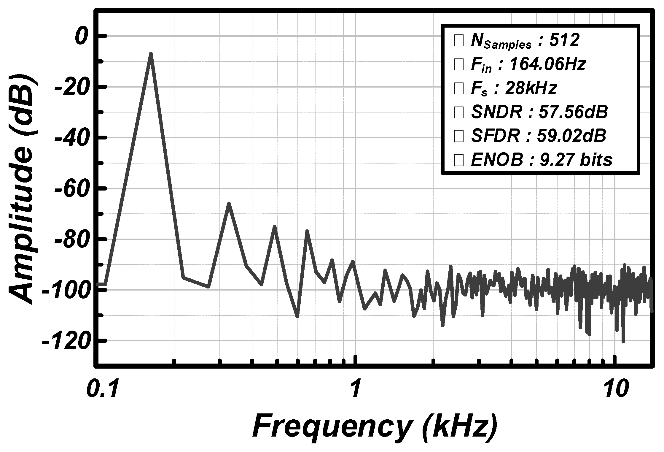
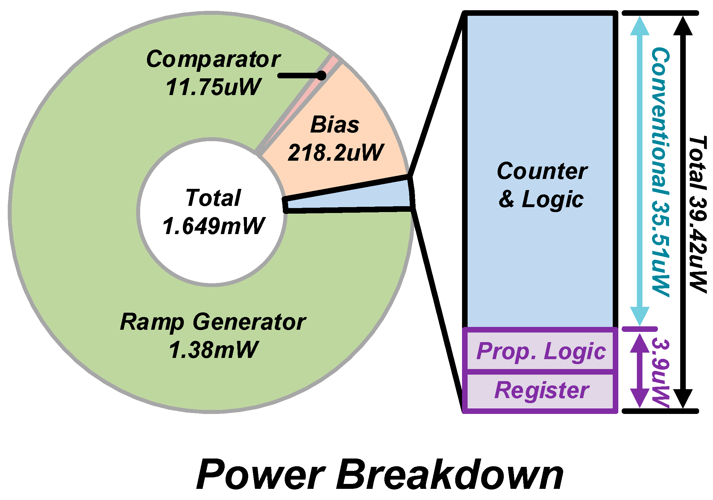
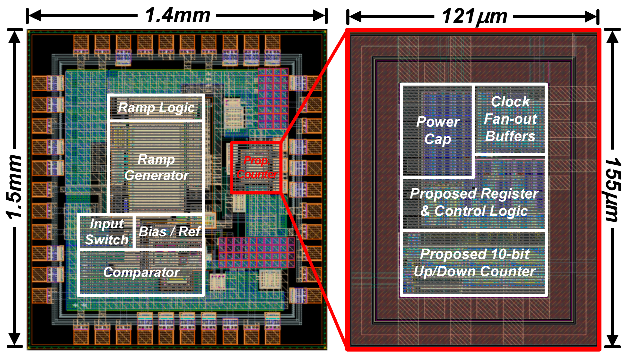
4. Simulation Results and Discussion

Figure 8 presents the post-simulation results of the proposed baseline calibration scheme, showing the cases when D[SN] is ‘0’ in Figure 8a and ‘1’ in Figure 8b. Here, the simulations were conducted using the TSMC 180 nm 1P6M CMOS process at a standard temperature of 300 K and at the typical process corner (tt). Furthermore, we incorporated transient noise ranging from 0.1 Hz to 500 kHz. VIN represents the output voltage of the gas sensor. The simulations were conducted by setting the initial VIN to different levels of 1.6VBL, 1.5VBL, and 1.4VBL, after which VIN was increased at a constant slope. In Figure 8a, where the gas is introduced at a voltage level higher than VBL, D[SN] outputs ‘0’, indicating a positive output code value. During the baseline readout section, the ØRST signal triggers the reset of the SS ADC’s counter initial value (DOUT = 0). With the ØU/D signal at ‘LOW’, the proposed counter performs down counting during SS A/D conversion, outputting codes ‘−631’, ‘−561’, and ‘−491’ for 1.6VBL, 1.5VBL, and 1.4VBL, respectively. Subsequently, DOUT is stored as DBL in DREG upon triggering ØRCLK. From the signal readout section onwards, the ØU/D signal switches to ‘HIGH’, and the counter engages in up counting during SS A/D conversion. When ØUPDE is triggered, the counter’s initial value is updated with the stored DBL, and SS A/D conversion is performed based on this value. The simulation shows that regardless of the initial condition decreasing from 1.6VBL to 1.4VBL, the counter’s output, DOUT, increases uniformly in response to the input’s consistent slope. Similarly, in Figure 8b, under conditions where the input is introduced at a voltage level lower than VBL, D[SN] outputs ‘1’, resulting in negative output code values. It is observed that for different VBL levels, DOUT decreases uniformly in response to inputs that decrease with the same rate. This simulation demonstrates the effectiveness of the proposed calibration technique in maintaining consistent signal extraction across varying baseline levels, showcasing the robustness of the SS A/D conversion process within the gas sensor system. The ability to adjust the counter’s initial value according to the stored DBL ensures accurate signal processing and calibration, affirming the potential of this method to reduce computational demands and enhance the overall performance and response time of the gas sensor system. Furthermore, the proposed baseline calibration scheme is versatile and can be applied to a variety of gas sensor types. It is particularly beneficial for addressing issues of initial value dispersion that can occur even among sensors of the same type [26,27,28].
Figure 9 presents the fast Fourier transform (FFT) analysis results to evaluate the dynamic performance of the proposed SS ADC with the baseline calibration scheme. FFT is derived from post-simulation based on 512 samples of a sinusoidal input signal of 164.06 Hz (FIN), in consideration of the gas sensor’s slow transient response. The peak-to-peak voltage of the sine wave (VIN) was set to 1.2 V, within the ADC’s input range, and the ADC’s sampling frequency (FS) was simulated at 28 kHz. Here, the FFT output is displayed on a logarithmic scale along the x-axis, considering the low input frequency. Additionally, the post-simulation was conducted at room temperature (300 K), including transient noise with a frequency range from 0.1 Hz up to 500 kHz. As a result, the proposed SS ADC achieved a signal-to-noise and distortion ratio (SNDR) of 57.56 dB, resulting in an effective number of bits (ENOB) of 9.27 bits and a spurious-free dynamic range (SFDR) of 59.02 dB.
Figure 10 displays a post-simulation result for differential non-linearity (DNL) and integral non-linearity (INL) of the proposed SS ADC, sampled at an Fs of 28 kHz. The DNL characteristics range from a maximum of +0.259 LSB to a minimum of −0.263 LSB. Meanwhile, the INL characteristics are shown to range from a maximum of +0.868 LSB to a minimum of −0.122 LSB.
Figure 11 illustrates the total power consumption of the proposed SS ADC. It comprises several components: the comparator, ramp generator, biasing circuit, and counter, resulting in a total power consumption of 1.649 mW. The counter, embedded with the proposed baseline calibration scheme, consumes a total of 39.42 μW. This figure represents an approximate 11% increase compared to the conventional counter structure, but it only constitutes about 0.24% of the total power consumption. Moreover, since the proposed SS ADC performs baseline calibration during the gas sensor signal extraction, it can actually be considered to offer a power-saving benefit when digital computing resources are taken into account.
Table 1 presents a comparison between the conventional counter and the proposed counter, detailing the differences in logic, the number of transistors, and area usage. Specifically, the proposed counter includes an additional T-FF for the MSB sign bit, and an 11-bit D-FF register for storing the baseline code. It also includes 31 MUX switches to facilitate the up/down counter function and to control the reset and preset of the T-FFs. This addition of logic results in an increase in the total number of transistors from 438 to 1222. However, when considering the overall chip area, the actual increase in area is only about 2%, which is negligible in the total chip area. This indicates that the proposed scheme can implement an effective gas sensor baseline calibration function with a minimal increase in area cost.
Figure 12 depicts the layout of the proposed SS ADC with the baseline calibration scheme. It is fabricated using a 180 nm standard CMOS process. The entire chip occupies an area of 1.4 mm by 1.5 mm. Within this chip, the area specifically allocated for the proposed counter measures 121 µm by 155 µm. Table 2 provides a performance summary. Specifically, the performance of gas sensors is directly linked to the characteristics of the sensitive materials used, the heating process employed to enhance sensitivity, and the susceptibility to transient noise from external sources. These factors critically influence the reliability of the initial baseline conversion and, consequently, the overall system performance adopting the proposed baseline calibration scheme. Hence, there is a clear necessity for the development of robust algorithms capable of mitigating such challenges. Future research will be dedicated to exploring advanced algorithmic solutions that address these issues, aiming to enhance the resilience and accuracy of gas sensor systems.

5. Conclusions

This work introduces an SS ADC design integrated with a simple but strong baseline calibration scheme to enhance the accuracy and reliability of gas sensor readings. Various simulation results confirmed the efficacy of the proposed baseline calibration scheme, which implies that it would successfully address the challenge of baseline variability. This work offers a robust, precise, and power-efficient baseline calibration solution that meets the increasing demands for reliable gas detection in various applications.

Author Contributions

Conceptualization, J.-S.H. and H.-J.K.; methodology, J.-S.H. and H.-J.K.; software, J.-S.H.; validation, J.-S.H.; formal analysis, H.-J.K.; investigation, J.-S.H. and H.-J.K.; resources, J.-S.H. and H.-J.K.; data curation, J.-S.H.; writing—original draft preparation, J.-S.H. and H.-J.K.; writing—review and editing, H.-J.K.; visualization, J.-S.H.; supervision, H.-J.K.; project administration, H.-J.K.; funding acquisition, H.-J.K. All authors have read and agreed to the published version of the manuscript.

Funding

This study was supported by the Research Program funded by the SeoulTech (Seoul National University of Science and Technology).

Data Availability Statement

All data underlying the results are available as part of the present article and no additional source data are required.

Conflicts of Interest

The authors declare no conflicts of interest.

References

  1. Spirjakin, D.; Baranov, A.; Akbari, S. Wearable Wireless Sensor System with RF Remote Activation for Gas Monitoring Applications. IEEE Sens. J. 2018, 18, 2976–2982. [Google Scholar] [CrossRef]
  2. Kim, J.G.; Bai, B.C. A Chemical Safety Assessment of Lyocell-Based Activated Carbon Fiber with a High Surface Area through the Evaluation of HCl Gas Adsorption and Electrochemical Properties. Separations 2024, 11, 79. [Google Scholar] [CrossRef]
  3. Christakis, I.; Tsakiridis, O.; Kandris, D.; Stavrakas, I. Air Pollution Monitoring via Wireless Sensor Networks: The Investigation and Correction of the Aging Behavior of Electrochemical Gaseous Pollutant Sensors. Electronics 2023, 12, 1842. [Google Scholar] [CrossRef]
  4. Neri, G. First Fifty Years of Chemoresistive Gas Sensors. Chemosensors 2015, 3, 1–20. [Google Scholar] [CrossRef]
  5. Yamazoe, N. Toward innovations of gas sensor technology. Sens. Actuators B Chem. 2005, 108, 2–14. [Google Scholar] [CrossRef]
  6. Norzam, W.A.S.; Hawari, H.F.; Kamarudin, K.; Juffry, Z.H.M.; Hussein, N.A.A.; Gupta, M.; Abdullah, A.N. Mobile Robot Gas Source Localization Using SLAM-GDM with a Graphene-Based Gas Sensor. Electronics 2023, 12, 171. [Google Scholar] [CrossRef]
  7. Uma, S.; Shobana, M.K. Metal oxide semiconductor gas sensors in clinical diagnosis and environmental monitoring. Sens. Actuators A Phys. 2023, 349, 114044. [Google Scholar] [CrossRef]
  8. Nikolic, M.V.; Milovanovic, V.; Vasiljevic, Z.Z.; Stamenkovic, Z. Semiconductor Gas Sensors: Materials, Technology, Design, and Application. Sensors 2020, 20, 6694. [Google Scholar] [CrossRef] [PubMed]
  9. Krishna, K.G.; Parne, S.; Pothukanuri, N.; Kathirvelu, V.; Gandi, S.; Joshi, D. Nanostructured metal oxide semiconductor-based gas sensors: A comprehensive review. Sens. Actuators A Phys. 2022, 341, 113578. [Google Scholar] [CrossRef]
  10. Shaposhnik, A.V.; Moskalev, P.V.; Chegereva, K.L.; Zviagin, A.A.; Vasiliev, A.A. Selective gas detection of H2 and CO by a single MOX-sensor. Sens. Actuators B Chem. 2021, 334, 129376. [Google Scholar] [CrossRef]
  11. Furst, L.; Feliciano, M.; Frare, L.; Igrejas, G. A Portable Device for Methane Measurement Using a Low-Cost Semiconductor Sensor: Development, Calibration and Environmental Applications. Sensors 2021, 21, 7456. [Google Scholar] [CrossRef] [PubMed]
  12. Kim, J.N.; Kim, H.J. A Chemoresistive Gas Sensor Readout Integrated Circuit with Sensor Offset Cancellation Technique. IEEE Access 2023, 11, 85405–85413. [Google Scholar] [CrossRef]
  13. Ng, K.T.; Boussaid, F.; Bermak, A. A CMOS Single-Chip Gas Recognition Circuit for Metal Oxide Gas Sensor Arrays. IEEE Trans. Circuits Syst. I Regul. Pap. 2011, 58, 1569–1580. [Google Scholar] [CrossRef]
  14. Nazemi, H.; Joseph, A.; Park, J.; Emadi, A. Advanced Micro- and Nano-Gas Sensor Technology: A Review. Sensors 2019, 19, 1285. [Google Scholar] [CrossRef] [PubMed]
  15. Haugen, J.-E.; Tomic, O.; Kvaal, K. A calibration method for handling the temporal drift of solid state gas-sensors. Anal. Chim. Acta 2000, 407, 23–39. [Google Scholar] [CrossRef]
  16. Grassi, M.; Malcovati, P.; Baschirotto, A. A 141-dB Dynamic Range CMOS Gas-Sensor Interface Circuit Without Calibration With 16-Bit Digital Output Word. IEEE J. Solid-State Circuits 2007, 42, 1543–1554. [Google Scholar] [CrossRef]
  17. Lee, D.Y.; Yu, J.B.; Byun, H.G.; Kim, H.J. Chemoresistive Sensor Readout Circuit Design for Detecting Gases with Slow Response Time Characteristics. Sensors 2022, 22, 1102. [Google Scholar] [CrossRef] [PubMed]
  18. Choi, S.; Park, C.S.; Chae, H.Y.; Oh, B.; Lee, J.; Kwon, Y.M.; Baik, J.M.; Shin, H.; Kim, J.J. A Wide Dynamic Range Multi-Sensor ROIC for Portable Environmental Monitoring Systems With Two-Step Self-Optimization Schemes. IEEE Trans. Circuits Syst. I Regul. Pap. 2021, 68, 2432–2443. [Google Scholar] [CrossRef]
  19. Kim, H.J. 11-bit Column-Parallel Single-Slope ADC With First-Step Half-Reference Ramping Scheme for High-Speed CMOS Image Sensors. IEEE J. Solid-State Circuits 2021, 56, 2132–2141. [Google Scholar] [CrossRef]
  20. Zhang, H.; Zhang, Z.; Li, Z.; Han, H.; Song, W.; Yi, J. A chemiresistive-potentiometric multivariate sensor for discriminative gas detection. Nat. Commun. 2023, 14, 3495. [Google Scholar] [CrossRef]
  21. Korotcenkov, G.; Cho, B.K. Instability of metal oxide-based conductometric gas sensors and approaches to stability improvement (short survey). Sens. Actuators B Chem. 2011, 156, 527–538. [Google Scholar] [CrossRef]
  22. Ciciotti, F.; Buffa, C.; Radogna, A.V.; Francioso, L.; Capone, S.; Gaggl, R.; Baschirotto, A. A 450-µA 128-dB Dynamic Range A/D CMOS Interface for MOX Gas Sensors. IEEE Sens. J. 2019, 19, 12069–12078. [Google Scholar] [CrossRef]
  23. Boukhayma, A.; Peizerat, A.; Enz, C. A Sub-0.5 Electron Read Noise VGA Image Sensor in a Standard CMOS Process. IEEE J. Solid-State Circuits 2016, 51, 2180–2191. [Google Scholar] [CrossRef]
  24. Kłosowski, M. A Power-Efficient Digital Technique for Gain and Offset Correction in Slope ADCs. IEEE Trans. Circuits Syst. II Express Briefs 2020, 67, 979–983. [Google Scholar] [CrossRef]
  25. Park, K.; Yeom, S.; Kim, S.Y. Ultra-Low Power CMOS Image Sensor With Two-Step Logical Shift Algorithm-Based Correlated Double Sampling Scheme. IEEE Trans. Circuits Syst. I Regul. Pap. 2020, 67, 3718–3727. [Google Scholar] [CrossRef]
  26. An, N.; Li, Y.; Zhang, H.; Liang, Y.; Tan, T.; Guo, Y.; Liu, Z.; Liu, M.; Guo, Y.; Wu, Y.; et al. Brillouin lasers in a graphene microresonator for multispecies and individual gas molecule detection. APL Photonics 2023, 8, 100801. [Google Scholar] [CrossRef]
  27. Guo, Y.; Li, Z.; An, N.; Guo, Y.; Wang, Y.; Yuan, Y.; Zhang, H.; Tan, T.; Wu, C.; Peng, B.; et al. A Monolithic Graphene-Functionalized Microlaser for Multispecies Gas Detection. Adv. Mater. 2022, 34, 2207777. [Google Scholar] [CrossRef]
  28. Wang, Y.; Li, Y.; Li, Y.; Zhang, H.; Liu, Z.; Guo, Y.; Wang, Z.; He, J.; Guo, X.; Wang, Y.; et al. Noise canceled graphene-microcavity fiber laser sensor for ultrasensitive gas detection. Photon. Res. 2023, 11, A1–A9. [Google Scholar] [CrossRef]
Figure 1. Characteristic of baseline variation inherent in gas sensor.
Electronics 13 01252 g001
Figure 2. (a) Simplified block diagram of conventional SS ADC and (b) its operational timing diagram.
Electronics 13 01252 g002
Figure 3. Simplified conventional N-bit up counter for SS A/D conversion.
Electronics 13 01252 g003
Figure 4. Simplified schematic of proposed SS A/D counter with baseline calibration scheme.
Electronics 13 01252 g004
Figure 5. Operation examples of proposed counter with baseline calibration scheme: (a) case for D[SN] = ‘0’ and (b) case for D[SN] = ‘1’.
Electronics 13 01252 g005
Figure 6. Operational algorithm for proposed SS ADC with baseline calibration scheme.
Electronics 13 01252 g006
Figure 7. Explanation for gas sensor signal extraction using proposed baseline calibration scheme.
Electronics 13 01252 g007
Figure 8. Simulation results of proposed baseline calibration scheme: (a) case for D[SN] = ‘0’ and (b) case for D[SN] = ‘1’.
Electronics 13 01252 g008
Figure 9. Fast Fourier transform analysis results of proposed SS ADC with baseline calibration scheme.
Electronics 13 01252 g009
Figure 10. (a) Differential non-linearity and (b) integral non-linearity.
Electronics 13 01252 g010
Figure 11. Power consumption of proposed SS ADC.
Electronics 13 01252 g011
Figure 12. Layout of proposed SS ADC.
Electronics 13 01252 g012
Table 1. Comparison of conventional and proposed counter.
ParameterConventional CounterProposed Counter and Register
Total Number of TransistorsCounter Unit Cell
(T-FF)
420 (×10 units)462 (×11 units)
Counter Unit Cell
(T-FF)
0308 (×11 units)
MUX Switch0434 (×31 units)
Control Logic Gate1818
4381222
Digital Power Consumption35.51 μW39.42 μW
Area Consumption of Counter 121   μ m   ×   113   μ m = 0.136 mm2 121   μ m   ×   155   μ m = 0.187 mm2
Unique Function-Baseline Digital Calibration
Table 2. Performance summary.
ParameterValue
Technology0.18 μm 1P6M CMOS Process
Supply Voltages2.8 V (Analog), 1.8 V (Digital)
ADC Input Range1.2 V
Power Consumption1.649 mW
ADC Resolution10 bits
SNDR57.56 dB @Fin = 164.06 Hz
ENOB9.27 bits @Fin = 164.06 Hz
DNL+0.259/−0.263
INL+0.868/−0.122
Sampling Rate28 kHz
Sensing TypeResistance
Sensing Range10~120 kΩ
Unique FunctionBaseline Digital Calibration
Disclaimer/Publisher’s Note: The statements, opinions and data contained in all publications are solely those of the individual author(s) and contributor(s) and not of MDPI and/or the editor(s). MDPI and/or the editor(s) disclaim responsibility for any injury to people or property resulting from any ideas, methods, instructions or products referred to in the content.

