Abstract
In this paper, the temperature dependence of single event upset (SEU) cross-section in 28 nm embedded Static Random Access Memory (SRAM) of System in Package (SiP) was investigated. An atmospheric neutron beam with an energy range of MeV~GeV was utilized. The SEU cross-section increased by 39.8% when the temperature increased from 296 K to 382 K. Further Technology Computer Aided Design (TCAD) simulation results show that the temperature has a weak impact on the peak pulse current, which is mainly caused by the change of bipolar amplification effect with temperature. As the temperature increases, the critical charge of the device decreases by about 4.8%. The impact of temperature on the SEU cross-section is determined competitively by the peak pulse current and the critical charge. The impact of temperature on critical charge is expected to become more severe as the feature size is further advanced.
1. Introduction
With the rapid development of microelectronics technology, the feature size and operating voltage of electronic devices are decreasing, the operating frequency is increasing, and the number of devices per unit area is also increasing, which results in the single event effect (SEE) induced by atmospheric neutrons in aviation and ground electronic systems becoming more and more significant, and the reliability problems caused by this have attracted a lot of attention [1]. In recent years, airplane malfunctions and supercomputing data failures induced by atmospheric neutrons have become commonplace. In the aviation environment, atmospheric neutron-induced SEE can lead to system state errors and data upset, thus posing a considerable threat to the reliability of electronic devices, which can, in turn, jeopardize human life safety [2,3,4,5].
In the aviation environment, electric devices are exposed to atmospheric neutron radiation and temperature extremes (temperatures on the sunlit side of the device can be over 400 K, while temperatures on the shaded side can be as low as 90 K). Temperature affects the carrier transport process and the collisional ionization process inside the semiconductor device, which in turn leads to changes in the charge collection process inside the device [6]. Simulation work on Si p+/n/n+ diodes shows a significant temperature dependence of the transient current induced by heavy ions [7,8]. Liu and his coworkers conducted SEU irradiation of C12 heavy ions for 0.5-micron partially depleted Silicon-On-Insulator (SOI) SRAM devices. They found that the single event cross-section of the SRAM devices increased by 98% when the operating temperature was increased from 293 K to 388 K [9]. Cai and his coworkers investigated the temperature dependence of the SEU cross-section of commercial 0.15-micron Thin Film Transistor (TFT) SRAMs in the temperature range of 215–353 K. It was found that the SEU cross-section hardly varied with the temperature in the saturated region of the cross-section. In contrast, in the rising region of the cross-section, the SEU cross-section increased by 257% at the incidence of the Cl particles [10]. TCAD simulation results of charge sharing in 130 nm Complementary Metal Oxide Semiconductor (CMOS) technology devices show an increase in charge sharing collection with increasing temperature [11]. M. Bagatin and his coworkers irradiated commercial SRAMs with thermal and wide-spectrum neutron beams, studying the impact of temperature on the soft error rate. The experimental data, simulations, and analytical modeling show that, depending on the device, temperature may or may not increase the soft error sensitivity by a modest amount [12]. J. Cao et al. investigated the variation of SET pulse widths (irradiation by alpha particles) on 7 nm bulk FinFET D-FF in the temperature range of 300–360 K. The experimental results show that the SET pulse width at the 7 nm node is significantly affected by temperature [13]. Cai et al. investigated the variation of SET pulse width of 16 nm bulk FinFET inverter chain at different temperatures. The results show that an increase in temperature enhances the parasitic bipolar effect of the bulk FinFET technology, leading to an increase in the SET pulse width [14]. However, due to the lack of available spallation neutron sources, the above-mentioned research results on the impact of temperature on the SEE are based on heavy ions, and there is a lack of research on the case of the impact of temperature on the SEE of SRAM devices under atmospheric neutron radiation conditions. Unlike heavy ions, neutrons are not electrically charged, but when incident on the device, a nuclear reaction produces secondary particles, which react with the device to cause SEE [15,16]. The SEE induced by neutrons consists of the following two aspects: thermal neutrons react with B10 to produce alpha particles and heavy ions [17]; high-energy and medium-energy neutrons react with materials such as Si in the device to produce recoil heavy nuclei, protons, etc. [18].
In this paper, an Atmospheric Neutron Irradiation Spectrometer (ANIS) [19], which was jointly constructed by the China Electronic Product Reliability and Environmental Testing Research Institute (CEPREI) and China Spallation Neutron Source (CSNS), was used to conduct variable experiments on 28 nm static random memories under different temperature conditions and investigate the variation of SEU in 28 nm embedded SRAM of SiP in the temperature range of 296–382 K. The transient pulse currents are also simulated using TCAD simulation software to analyze their physical mechanisms.
2. Experiments at the ANIS
2.1. Experimental Device
Memory is an important part of microelectronic devices. Atmospheric neutron SEE was investigated using SRAM embedded in SiP as test board. The SRAM adopts the CMOS process, and its core memory cell is a 6-transistor structure with a supply voltage of 0.9 V and a feature size of 28 nm. The testing capacity of SRAM is 1020 KB.
2.2. Experimental Platform
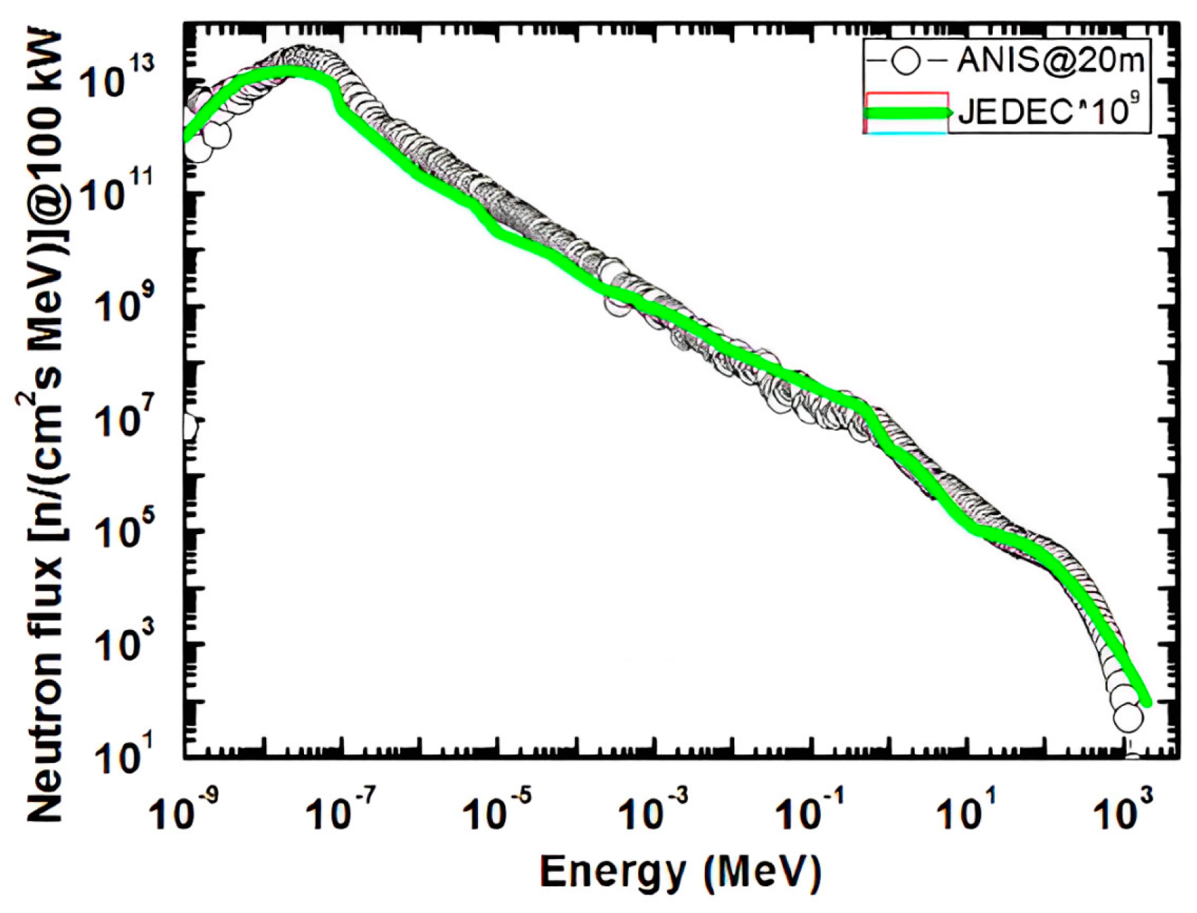
JEDEC standards refer to a series of standards established by the Joint Electron Device Engineering Council (JEDEC) to regulate semiconductor products, technologies, and testing methods [20]. According to the JEDEC Standard JESD89A, the integrated neutron flux at the terrestrial level is equal to 20 n/(cm2·h) in the energy range > 1 MeV. This value is referenced to New York City at sea level, under conditions of average solar activity. Figure 1 shows ANIS’s simulated differential neutron spectrum at 20 m, with 100 kW of proton beam power. The Joint Electron Device Engineering Council (JEDEC) neutron spectrum is also presented for comparison. The differential spectrum matches the JEDEC standard well in the full energy range. In addition, the neutron flux is approximately 109 greater than JEDEC standards. Therefore, it is very suitable for the study of atmospheric neutron SEE.

Figure 1.
The differential neutron spectrum compared with the JEDEC standard [19].
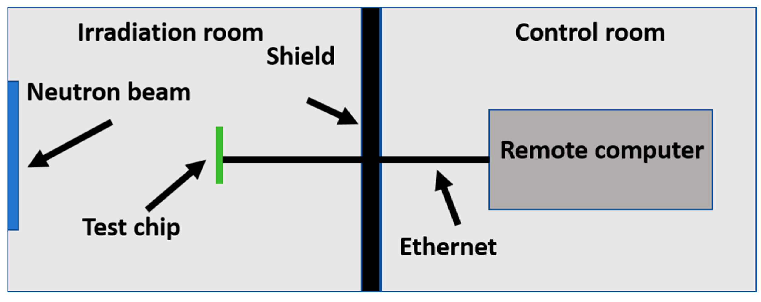
The experimental site consists of two parts: the irradiation room, and the control room, where the tester writes, reads, and detects the experimental data of the test system through the host computer. The irradiation and control rooms are connected via Ethernet, as shown in Figure 2.
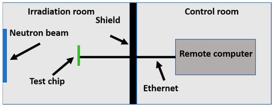
Figure 2.
Laboratory layout diagram.
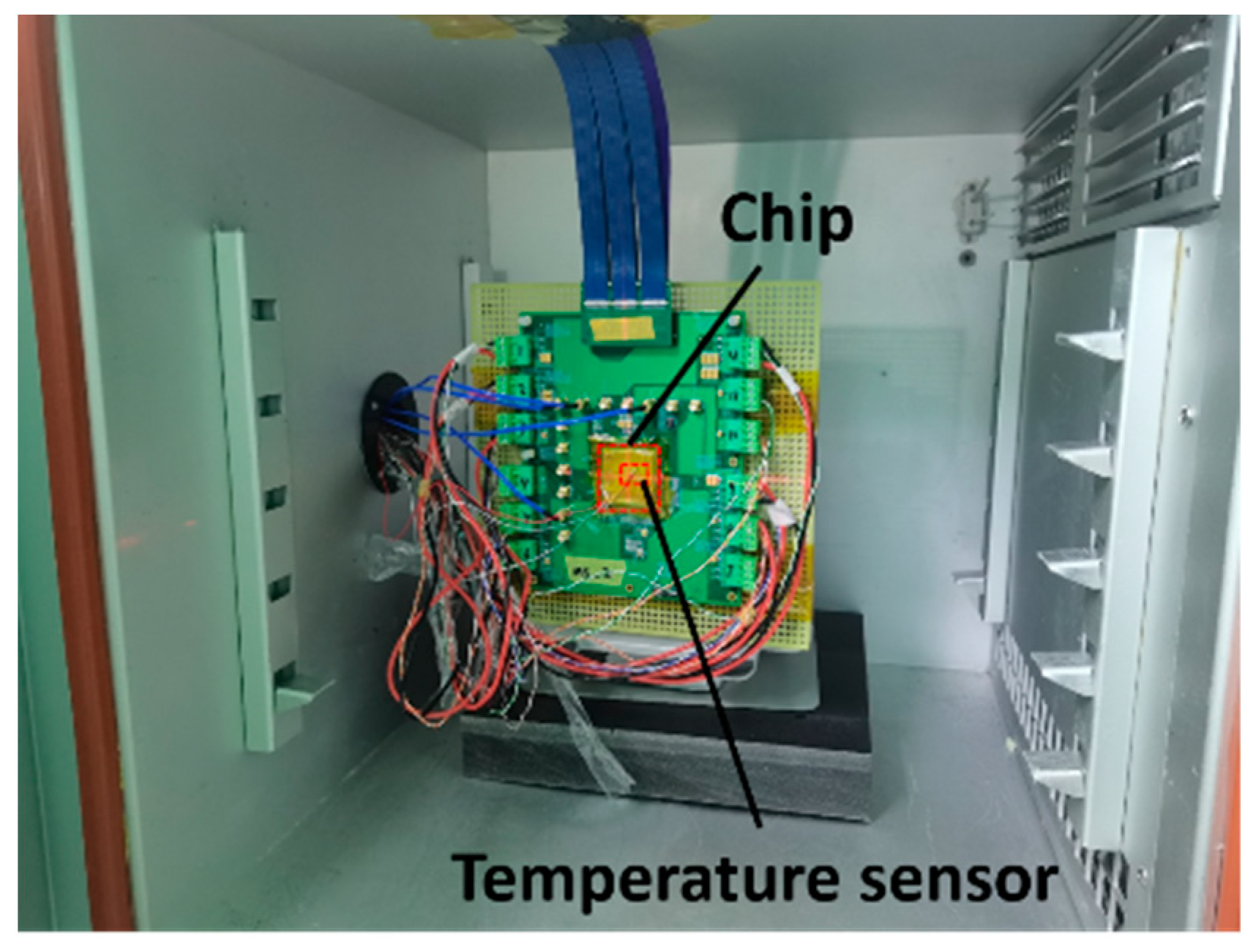
The experiments were conducted at room temperature as well as high temperature. The test board was placed in a thermal cycling chamber to heat it during the experiment. Considering the memory’s working temperature range, the temperature points selected for the thermal cycling chamber were 280, 300, 330, and 360 K, respectively. The control panel of the thermal cycling chamber is outside the irradiation room, so the temperature of the thermal cycling chamber can be controlled directly from the outside. Considering the heat of the chip, in order to detect the temperature of the test board in real-time, one side of the PT100 temperature sensor was pasted on the surface of the chip, and the other side was connected to the PID digital display temperature controller. The changes in the temperature figures on the digital display temperature controller can be observed from the monitoring of the control room. During the experiment, the chip’s temperature was 296, 322, 351, and 382 K. When the temperature of the chip is kept constant, the experiment can be started. Figure 3 and Figure 4 show the experimental field diagram and the thermal chamber.
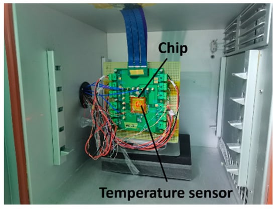
Figure 3.
Experimental field diagram.
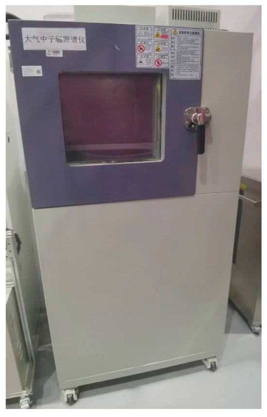
Figure 4.
Thermal chamber.
2.3. Experimental Method
The size of the neutron beam used in this experiment is 6 cm × 10 cm, and the flux rate of neutrons is about 0.85 × 10⁶ n/(cm2·s). During the experiment, the test board always faced the neutron source, and the neutrons in the experiments were vertically incident. Data 0xA5 was written during the experiment, and to ensure that the experimental data had reliability and ideal statistics, measurements were taken 2–3 times under the same conditions. The experiment was stopped when the number of errors reached 100 or more. The SEU detection includes static and dynamic tests; in order to detect whether the upsets occur in real-time, this experiment chose dynamic detection. The experimental data were written to the memory unit before irradiation, and the data in the memory were read back at intervals (Reading data every second). The number of error bits was counted by comparing the read-out data with the original data written one by one. The chip’s current was monitored in real-time during the experiment to avoid single event latch-up and burning the chip. The electric threshold was set. When the current of the chip exceeded the electric threshold, the single event latch-up was considered to have occurred. Then, it was necessary to repower up the daughter board and rewrite the experimental data.
2.4. Experimental Result
The experimental data are shown in Table 1.

Table 1.
Experimental data.
The SEU cross-section of SRAM is calculated as follows:
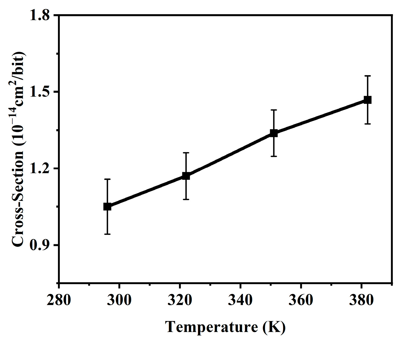
where is the SEU cross-section, NSEU is the number of upsets measured at the irradiated chip, C is the total capacity of the measured SRAM to store data, and φ is the total fluence of the atmospheric neutron. According to data provided by ANIS, the flux rate of atmospheric neutrons is 0.85 × 10⁶ n/(cm2·s). Figure 5 shows the variation of the SRAM SEU cross-section under different temperature conditions. When the temperature increases from 296 K to 382 K, the cross-section of SRAM increases from 1.05 × 10⁻¹⁴ cm2/bit to 1.468 × 10⁻¹⁴ cm2/bit, an increase of 39.8%. From the experimental results, the relationship between the upset cross-section and temperature appears to be approximately linear. Therefore, we conducted a linear fit and obtained the angular coefficient σ for the linear fit, which is 4.86 × 10⁻¹⁷ cm2/bit/K in this paper. The linear energy transfer (LET) value of secondary particles induced by atmospheric neutrons is very small, mainly causing soft errors, and no latch-up events were observed during the experiment, so it is considered that the experimental devices are not sensitive to latch-up under neutron irradiation. The SEU cross-section of the SRAM versus temperature depends on the transient pulse current and the electrical characteristics of the device, and the relationship between temperature and cross-section variation is approximately linear, which will be explained in the next section.
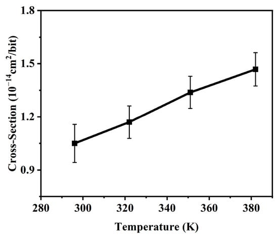
Figure 5.
Temperature dependence of SEU cross-section.
3. Discussion
In general, the impact of temperature on SEU depends firstly on the amount of charge deposited within the effective collection depth and secondly on the charge collection process as well as the electrical characteristics of the device, which are all functions of temperature [13,21]. The temperature changes the forbidden bandwidth of the material, which affects the amount of charge deposited by irradiated particle incidence in the adequate collection depth range. The physical mechanisms of charge collection include drift, diffusion, and bipolar amplification. Temperature changes the amount of charge collected by the three mechanisms [22]. Changing temperature changes the upset voltage of the device, and a decrease in the upset voltage reduces the critical charge of the device, thus affecting its SEU cross-section [10].
3.1. Temperature Dependence of Deposited Charge
An increase in temperature leads to a narrowing of the band-gap of Si, and a decrease in the band gap means that more electron-hole pairs are produced for the same linear energy transfer (LET) value of heavy ions. Therefore, the impact of temperature on the electron-hole pairs deposited by heavy ions into the device is mainly reflected in its impact on the band-gap. The variation of band-gap with temperature can be described by the following equation [23]:
where T is the absolute temperature, Eg(0) is the band-gap energy at 0 K, and α and β are material parameters. For silicon, α is 4.3 × 10⁻⁴ eV/K, and β is 636 K by default. We used default α and β values for all simulations, and the band-gap decreases from 1.1251 to 1.1018 eV when the temperature rises from 296 K to 382 K. According to [24], the average energy expended per ionized electron-hole pair in silicon is
As temperature increases from 296 K to 382 K, the average energy expended per ionized electron-hole pair in silicon decreases from 3.62 eV to 3.54 eV, suggesting that depositing the same energy increases the Coulomb charge by 2.26%.
3.2. Temperature Dependence of Charge Collection Efficiency
Changes in collected charge leads to variations in pulse current, which consists of two parts: pulse current peak and pulse current duration. Changes in the pulse current peak and duration will change the device’s LET threshold, thereby affecting the upset cross-section of the device. The total charge collected is the sum of the drift, diffusion, and bipolar amplification effect, and the impact of temperature on charge collection is reflected in the impact on each of these mechanisms [23]. Increased temperature leads to decreased mobility, and as a result, less charge is collected by drift. The drift charge determines the value of the peak pulse current. A change in temperature leads to a change in the diffusion length and change the charge collected by diffusion. The diffusion charge mainly determines the transient pulse current duration. An increase in temperature causes the bipolar amplification effect to be more significant, causing more charge to be collected. The bipolar amplification charge can affect the peak pulse value and the pulse current duration. The impact of temperature variation on the pulse current characteristics is investigated below from the above three points.
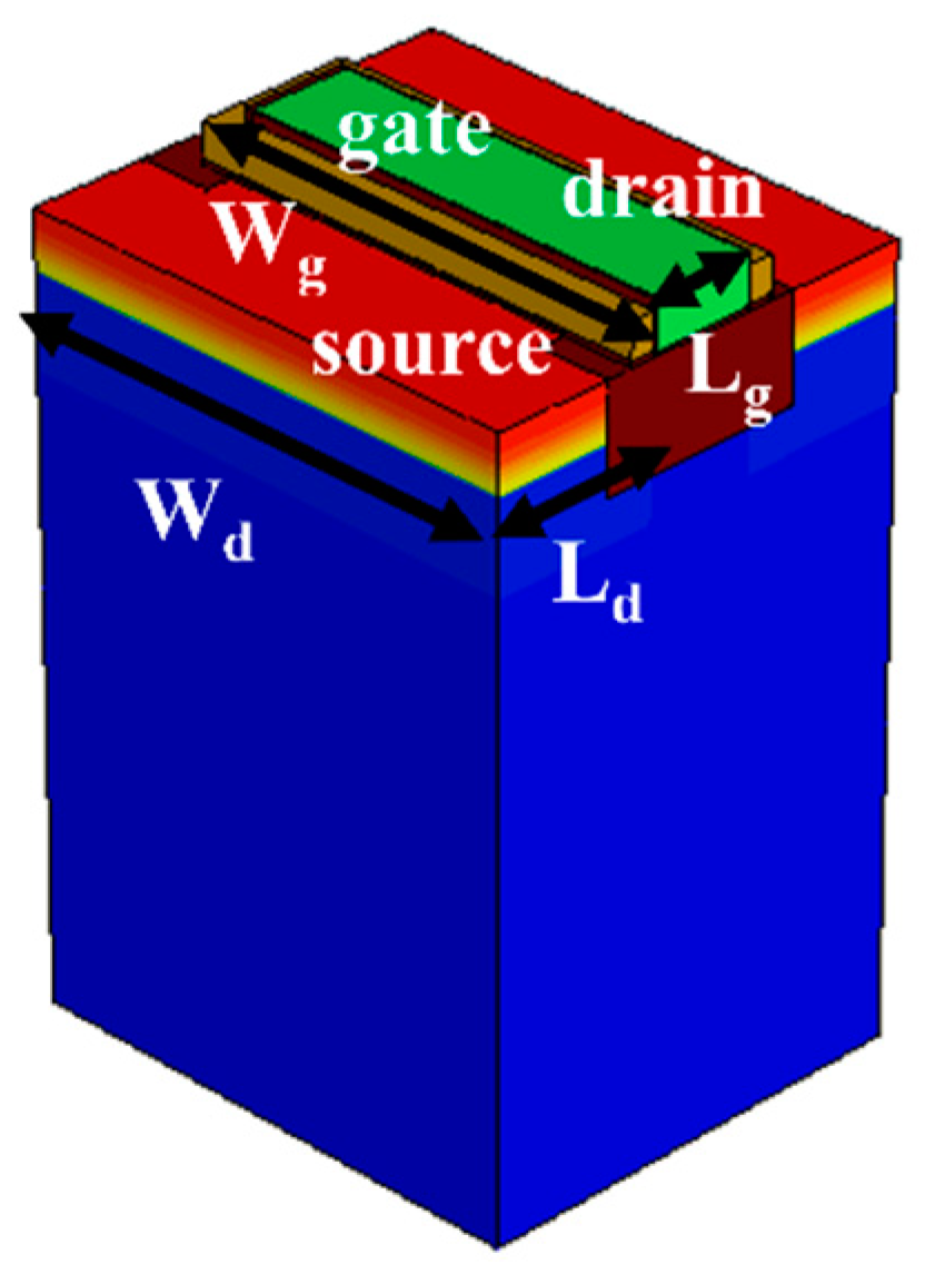
In this paper, Synopsys’ Sentaurus TCAD tool was used to analyze the single event charge collection mechanism of 28 nm MOSFET. The simulation model of the 3D device is given in Figure 6. The source/drain doping concentration of the device is 1 × 1019 cm−3, and the well doping concentration is 1 × 1017 cm−3. The relevant dimensional parameter values of the device are shown in Table 2. The single event transient response is most sensitive when the transistor is in the off state, so all simulations were performed with the device in the off state [25]. The model was calibrated to the SPICE model before the simulation started to make the established model closer to the physical characteristics of the actual device.

Figure 6.
3D physical model of the device.
Table 2.
Structural Parameters of Device.
The following physical models were used: (1) Fermi-Dirac statistics, (2) band-gap narrowing effect, (3) doping-dependent Shockley-Read-Hall (SRH) recombination and Auger recombination, (4) temperature, doping, electricfield and carrier-carrier-scattering impact on mobility, and (5) incident heavy ions were modeled using a Gaussian radial profile with a characteristic 1/e radius of 10 nm. A hydrodynamic model was used for carrier transport. Unless otherwise specified, default models and parameters provided by Sentaurus TCAD vN-2017.09-SP1 (Synopsys, Mountain View, CA, USA) were used.
Heavy ions were selected to incident vertically at the center of the drain region of the N-type device, and the temperature of the device was chosen to be 296, 322, 351, and 382 K, respectively. The LET values of secondary ions produced by the interaction of atmospheric neutrons with materials are relatively small. If the LET value is too small, it will not cause upset in the device. The number of ions with larger LET values is very limited, resulting in minimal impact on the devices. Therefore, ions with LET values of 1, 5, and 10 MeV·cm2/mg are selected for simulation. In studying the impact of bipolar amplification on the transient current of devices, the source is not doped. Therefore, the drain and channel can be approximated as a diode. Since the source electrode is not doped, it cannot inject electrons into the channel, eliminating the bipolar amplification effect. Therefore, the transient current of the diode represents drift diffusion current [22]. Subtracting the total charge from the drift-diffusion collected charge to get the bipolar amplification collected charge.
3.2.1. Temperature Dependence of Peak Pulse Current
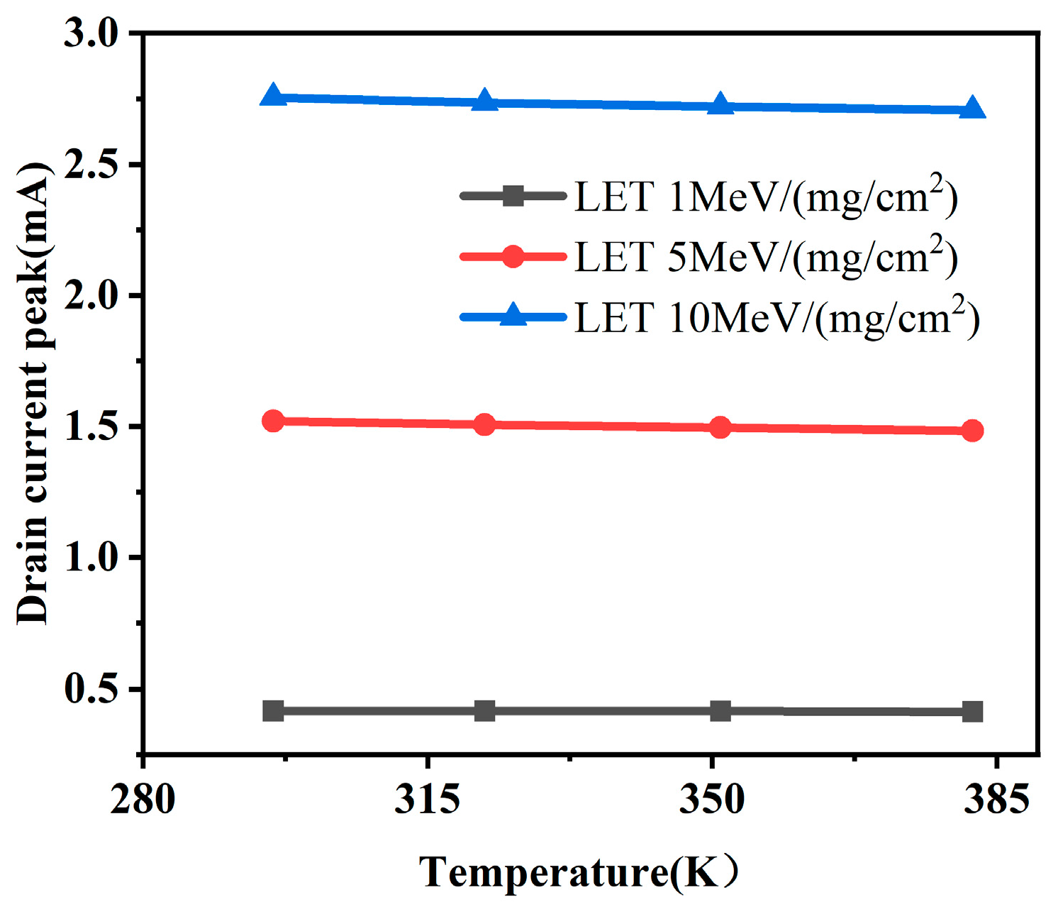
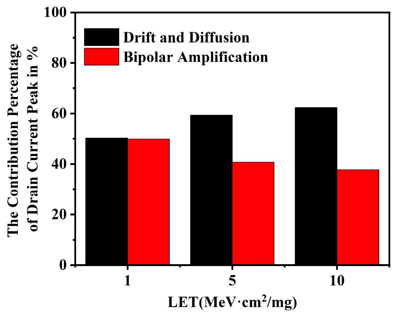
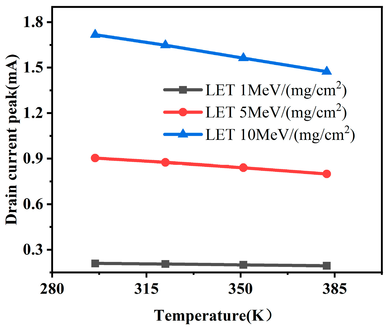
To visualize the relationship between peak pulse current and temperature, this paper plots the peak pulse current and the temperature as a curve in Figure 7. When the temperature increased from 296 K to 382 K, the peak pulse current with LET of 1, 5, and 10 Mev·cm2/mg decreased from 0.417, 1.521, and 2.755 mA to 0.414, 1.483, and 2.707 mA, which is a reduction of 0.7%, 2.5%, and 1.7%, respectively. As the LET increases, the total amount of peak pulse increases. To distinguish the contribution of bipolar amplification current and drift current to the current peak, the peak pulse current corresponding to the diode is divided by the peak pulse current of the overall device, as shown in Figure 8, with a temperature point of 296 K selected. As the LET value increases, the contribution of the drift current and the bipolar amplification current to the peak pulse current of the device shows different trends. When the LET value increases from 1 to 10 Mev·cm2/mg, the proportion of drift current increases from 50.2% to 62.3%, while the proportion of bipolar amplification current decreases from 49.8% to 37.7%.
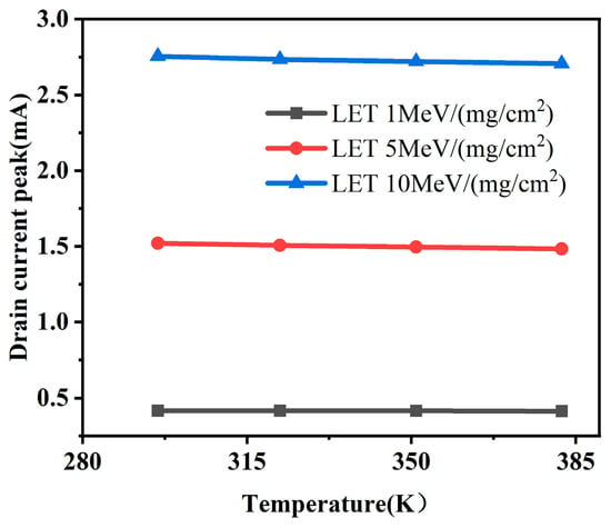
Figure 7.
Temperature dependence of peak pulse current.
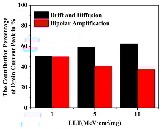
Figure 8.
Contribution of drift and bipolar amplification to pulse current peak (T = 296 K, Red: drift diffusion current, Black: bipolar amplification current).
Figure 9 shows the variation of the corresponding peak pulse current of the diode with temperature, which decreased from 0.209, 0.903, and 1.717 mA to 0.194, 0.799, and 1.473 mA for LET of 1, 5, and 10 Mev·cm2/mg when the temperature was increased from 296 K to 382 K. This is a reduction of 7.1%, 11.5%, and 14.2%, respectively. The impact of temperature on the peak current of the pulse is more significant when only drift current is considered. An explanation will be given below.
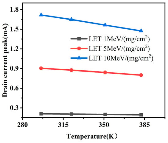
Figure 9.
Temperature dependence of drift pulse current.
The amount of charge collected by the drift is related to the carrier mobility, and the relationship between mobility and temperature can be given by the following equation:
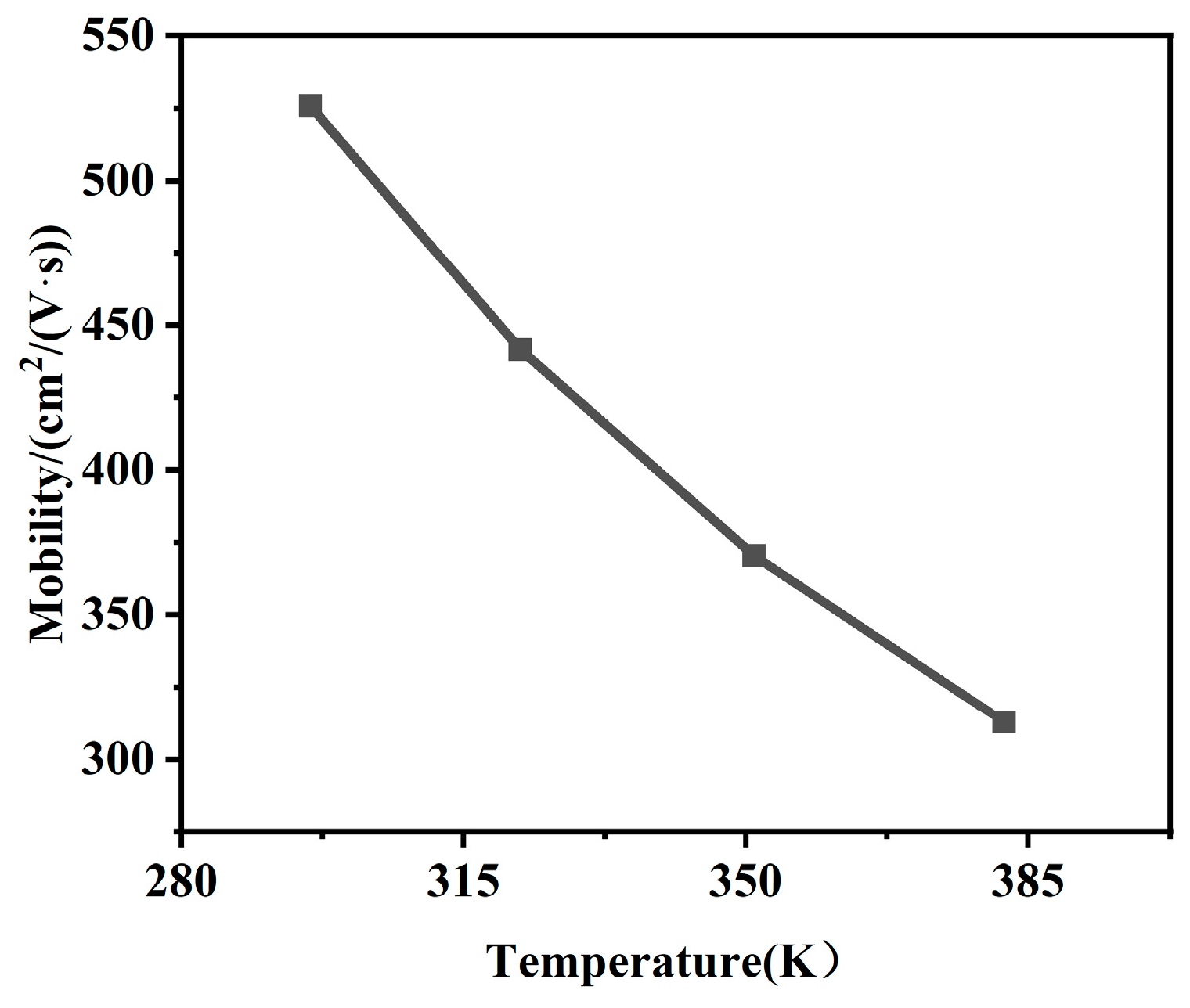
From the equation, it can be seen that mobility is inversely related to temperature. As the lattice vibration becomes more intense at higher temperatures, the probability of carriers receiving scattering increases, resulting in decreased mobility. As shown in Figure 10, the electron mobility around the drain decreases from 525.8 cm2/(V·s) to 313 cm2/(V·s) when the temperature increases from 296 K to 382 K. Thus, the amount of charge collected through the drift mechanism is consequently reduced, so the peak pulse current tends to decrease with increasing temperature for the overall device and the diode. As mentioned earlier, an increase in temperature will cause the bandgap of silicon to decrease, resulting in more electron-hole pairs being generated for the same amount of deposited energy. On the other hand, it will also cause the high energy hot carriers to create more holes through collisional ionization, and these extra holes will further elevate the potential after entering the well region, resulting in the bipolar amplification to collect more charges, which leads to a more significant bipolar amplification effect. Therefore, without considering the bipolar amplification effect, the peak pulse current is more significantly affected by temperature.
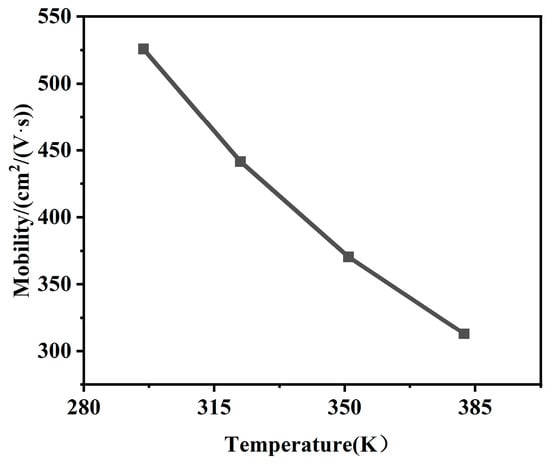
Figure 10.
Temperature dependence of electron mobility.
The smaller the pulse peak current, the larger the device’s LET threshold, resulting in a reduction in the upset cross-section of the device. From the analysis above, it can be inferred that an increase in temperature reduces drift current while increasing bipolar amplification current. A smaller drift current leads to a larger LET threshold, while a larger bipolar amplification current results in a smaller LET threshold, indicating a competitive relationship between the drift current and bipolar amplification current. From the simulation results, an increase in temperature raises the device’s LET threshold, thereby reducing the device’s upset cross-section.
3.2.2. Temperature Dependence of Pulse Current Duration
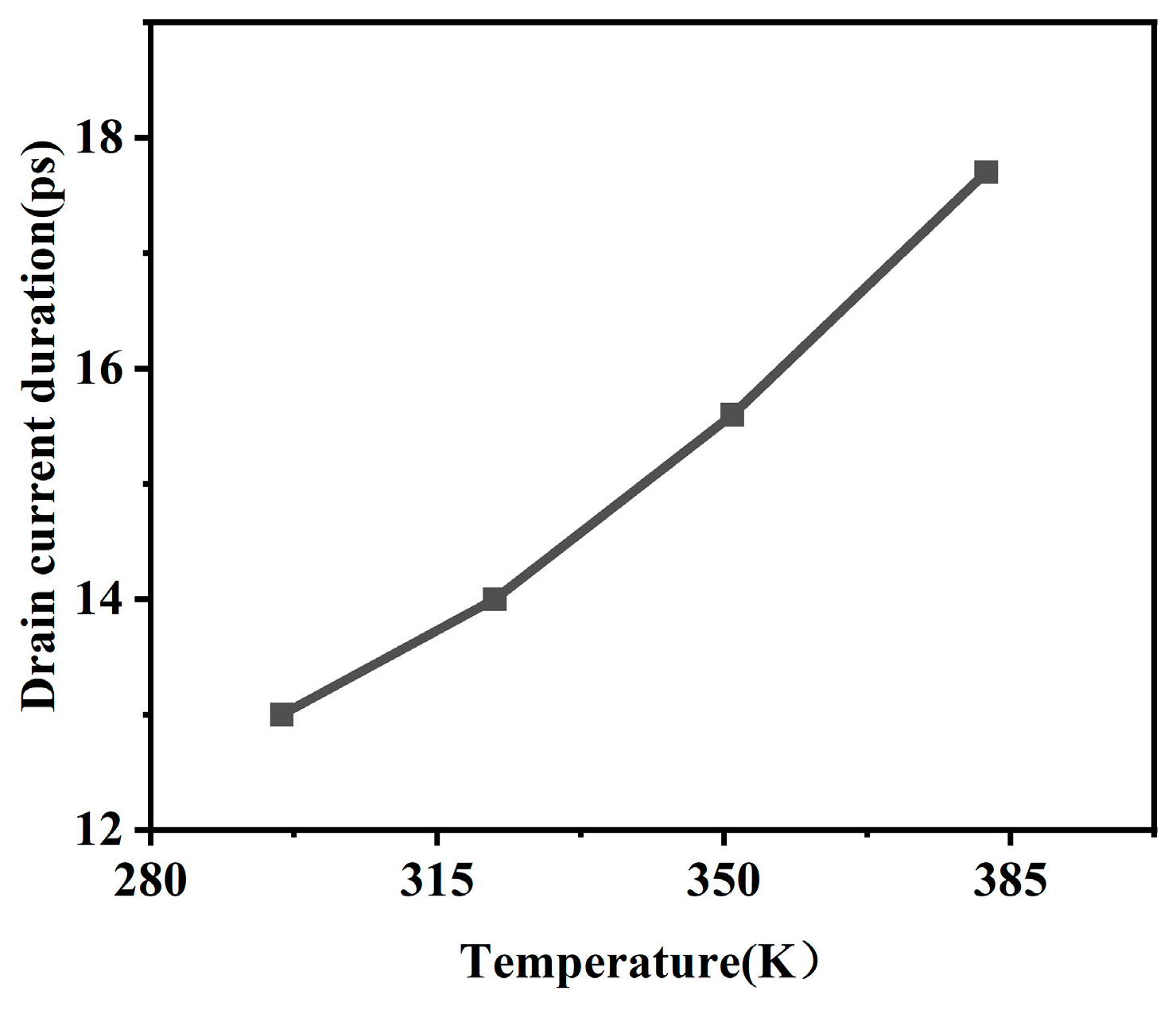
In this paper, the duration is defined as the time from the beginning of the pulse current until it first reaches 0 A. The relationship between pulse current duration and temperature is shown in Figure 11. The LET of the particles is 1 Mev·cm2/mg. When the temperature increased from 296 K to 382 K, the pulse current duration increased from 13 ps to 17.7 ps, an increase of 36%. The duration of the current is mainly determined by the diffusion mechanism and the bipolar amplification mechanism. As discussed previously, the bipolar amplification current increases with increasing temperature, which leads to an increase in duration. The variation of the diffusion coefficient with temperature can be derived from the following equation [26]:
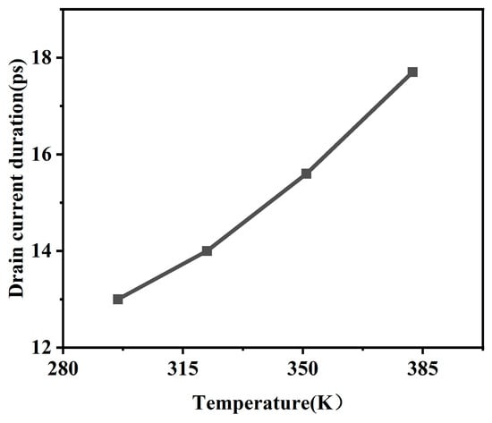
Figure 11.
Temperature dependence of pulse current duration.
When the temperature increases, the mobility and the diffusion coefficient decrease, which leads to an increase in the current duration. However, for SRAM, the current duration is up to tens of picoseconds, much longer than the upset time, so this duration will not be considered for SEU.
3.3. Temperature Dependence of Electrical Characteristics
Temperature changes will cause changes in the electrical characteristics of the device. When the particle is incident to the device, it will produce a transient voltage. If the transient voltage exceeds a specific value, it will cause the data to upset, called upset voltage. The upset voltage decreases with increasing temperature, while a decrease in the upset voltage decreases the LET threshold value of the device, which increases the SEU cross-section of the SRAM. The empirical relationship between upset voltage and temperature is as follows [10]:
T is the operating temperature of the device, K = dV⁄dT; Vupset0 is the upset voltage at 0 K, which is determined by the electrical characteristics of the device, and the linear relationship between the upset voltage and the temperature is −0.2 mV/k [10]. The critical charge can be estimated by the following equation:
Qc is the critical charge, is the gate capacitance, and the gate capacitance of the 28 nm transistor is generally 0.5 fF. According to Equation (7), it can be concluded that the relationship of the critical charge with the temperature is −1 × 10⁻³ fC/k. When the temperature rises from 296 K to 382 K, the critical charge decreases by 0.0086 fC. The relationship between critical charge and temperature is approximately linear, and the decrease in critical charge is the main reason for the increase in cross-section. Therefore, the relationship between temperature and cross-section variation also appears to be approximately linear.
Literature [27] based on a combination of large amounts of modeling and experimental data suggests that the critical charge and the characteristic dimensions of the transistor are squarely related:
Qc is the critical charge, and L is the feature size of the device. According to the above equation, the critical charge of 28 nm SRAM is 0.18 fC. When the temperature increased from 296 K to 382 K, the critical charge decreased by 4.8%. The critical charge of devices produced by different manufacturers will differ for the same feature size. Literature [28] gives that the critical charge of the device is about 0.8 fC for the 65 nm feature size and 0.1 fC for the 22 nm feature size, which is basically comparable to the above equations. The temperature dependence of the experimental device in this paper is more pronounced compared to the devices in the literature [12] (with a feature size of 180 nm), which is due to the fact that the critical charge decreases in square steps as the feature size decreases, and thus also leads to an increasingly severe effect of temperature on the critical charge, which is the main reason for the increase in the upset cross-section. As the feature size continues to decrease, the impact on the SEU cross-section of the decrease in critical charge from changing temperature will become more severe.
4. Conclusions
Based on the ANIS, the temperature dependence of the SEU cross-section in 28 nm embedded SRAM of SiP in the temperature range of 296–382 K was investigated. Under atmospheric neutron irradiation, the SEU cross-section increased from 1.05 × 10⁻¹⁴ cm2/bit to 1.468 × 10⁻¹⁴ cm2/bit, an increase of 39.8%, when the temperature was increased from 296 K to 382 K.
The variation of SEU cross-section with temperature is mainly caused by the combination of the variation of the electrical characteristics and the transient pulse current with temperature. The decrease of the peak pulse current increases the LET threshold, while the decrease of the critical charge decreases the LET threshold. Raising the LET threshold will decrease the upset cross-section, while lowering the LET threshold will increase the upset cross-section, both of which play a competitive relationship. TCAD simulation results show that when the temperature was increased from 296 K to 382 K, the transient pulse current of the device decreased by 0.7%, 2.5%, and 1.7% under the irradiation of particles with LET of 1, 5, and 10 Mev·cm2/mg, respectively. The temperature does not significantly impact it, which is mainly caused by the fact that the bipolar amplification effect becomes more significant with increasing temperature. By increasing the body contact, the bipolar amplification effect on the peak value of the transient pulse current can be reduced, which can enhance the upset resistance of the device and its reliability. The pulse current duration up to tens of picoseconds, which is much longer than the SEU time, is not considered. As the temperature increases from 296 K to 382 K, the critical charge of the device decreases by about 4.8%. As the feature size advances further, the impact of changing temperature on the critical charge will become more significant. The relationship between critical charge and temperature is linear, and the decrease in critical charge is the main reason for the growth of the upset cross-section. Therefore, the relationship between upset cross-section and temperature is approximately linear. The above conclusions provide a theoretical basis for the widespread use of SRAM in aerospace environments at temperatures of 296–382 K and for future development of advanced SRAM.
Author Contributions
Conceptualization, S.Z.; Methodology, S.Z.; Software, S.Z., X.L. and H.Z.; Validation, Z.L. (Zhili Liu), G.G. and Q.Z.; Formal analysis, S.Z.; Investigation, S.Z.; Data curation, S.Z. and J.Y.; Writing—original draft, S.Z.; Writing—review & editing, Z.Z.; Supervision, Z.Z., Z.L. (Zhili Liu), G.G., Q.Z. and H.L.; Project administration, Z.Z., Z.L. (Zhifeng Lei), Z.L. (Zhili Liu), G.G. and Q.Z.; Funding acquisition, Z.Z. and Z.L. (Zhifeng Lei). All authors have read and agreed to the published version of the manuscript.
Funding
This work was supported by the National Natural Science Foundation of China (Grant Nos. 12175045, 12075065), the Key-Area Research and Development Program of Guangdong Province (Grant No. 2022B0701180002) and the Opening Project of Science and Technology on Reliability Physics and Application Technology of Electronic Component Laboratory.
Data Availability Statement
Data are contained within the article.
Acknowledgments
The authors sincerely thank colleagues of China Spallation Neutron Source for their great support and assistance during the experiment.
Conflicts of Interest
Authors Zhili Liu, Gaoying Geng and Qi Zhang were employed by the company The 58th Institute of China Electronics Technology Group Corporation. The remaining authors declare that the research was conducted in the absence of any commercial or financial relationships that could be construed as a potential conflict of interest.
References
- Abe, S.; Watanabe, Y. Analysis of Charge Deposition and Collection Caused by Low Energy Neutrons in a 25-Nm Bulk CMOS Technology. IEEE Trans. Nucl. Sci. 2014, 61, 3519–3526. [Google Scholar] [CrossRef]
- Hubert, G.; Bezerra, F.; Nicot, J.-M.; Artola, L.; Cheminet, A.; Valdivia, J.-N.; Mouret, J.-M.; Meyer, J.-R.; Cocquerez, P. Atmospheric Radiation Environment Effects on Electronic Balloon Board Observed During Polar Vortex and Equatorial Operational Campaigns. IEEE Trans. Nucl. Sci. 2014, 61, 1703–1709. [Google Scholar] [CrossRef]
- Dyer, C.; Hands, A.; Ryden, K.; Lei, F. Extreme Atmospheric Radiation Environments and Single Event Effects. IEEE Trans. Nucl. Sci. 2018, 65, 432–438. [Google Scholar] [CrossRef]
- Normand, E. Single Event Upset at Ground Level. IEEE Trans. Nucl. Sci. 1996, 43, 2742–2750. [Google Scholar] [CrossRef]
- Normand, E. Single-Event Effects in Avionics. IEEE Trans. Nucl. Sci. 1996, 43, 461–474. [Google Scholar] [CrossRef]
- Gadlage, M.J.; Ahlbin, J.R.; Ramachandran, V.; Gouker, P.; Dinkins, C.A.; Bhuva, B.L.; Narasimham, B.; Schrimpf, R.D.; McCurdy, M.W.; Alles, M.L.; et al. Temperature Dependence of Digital Single-Event Transients in Bulk and Fully-Depleted SOI Technologies. IEEE Trans. Nucl. Sci. 2009, 56, 3115–3121. [Google Scholar] [CrossRef]
- Laird, J.S.; Hirao, T.; Onoda, S.; Mori, H.; Itoh, H. Temperature Dependence of Heavy Ion-Induced Current Transients in Si Epilayer Devices. IEEE Trans. Nucl. Sci. 2002, 49, 1389–1395. [Google Scholar] [CrossRef]
- Guo, G.; Hirao, T.; Laird, J.S.; Onoda, S.; Wakasa, T.; Yamakawa, T.; Kamiya, T. Temperature Dependence of Single-Event Transient Current Induced by Heavy-Ion Microbeam on p/Sup +//n/n/Sup +/ Epilayer Junctions. IEEE Trans. Nucl. Sci. 2004, 51, 2834–2839. [Google Scholar] [CrossRef]
- Liu, T.; Liu, J.; Geng, C.; Zhang, Z.; Zhao, F.; Tong, T.; Sun, Y.; Su, H.; Yao, H.; Gu, S.; et al. Influence of Deposited Energy in Sensitive Volume on Temperature Dependence of SEU Sensitivity in SRAM Devices. In Proceedings of the 2013 14th European Conference on Radiation and Its Effects on Components and Systems (RADECS), Oxford, UK, 23–27 September 2013; IEEE: Oxford, UK, 2013; pp. 1–6. [Google Scholar]
- Cai, L.; Guo, G.; Liu, J.-C.; Fan, H.; Shi, S.-T.; Wang, H.; Wang, G.-L.; Shen, D.-J.; Hui, N.; He, A.-L. Experimental Study of Temperature Dependence of Single-Event Upset in SRAMs. Nucl. Sci. Tech. 2016, 27, 16. [Google Scholar] [CrossRef]
- Liu, B.; Chen, S.; Liang, B.; Liu, Z.; Zhao, Z. Temperature Dependency of Charge Sharing and MBU Sensitivity in 130-nm CMOS Technology. IEEE Trans. Nucl. Sci. 2009, 56, 2473–2479. [Google Scholar] [CrossRef]
- Bagatin, M.; Gerardin, S.; Paccagnella, A.; Andreani, C.; Gorini, G.; Frost, C.D. Temperature Dependence of Neutron-Induced Soft Errors in SRAMs. Microelectron. Reliab. 2012, 52, 289–293. [Google Scholar] [CrossRef]
- Cao, J.; Xu, L.; Wen, S.-J.; Fung, R.; Narasimham, B.; Massengill, L.W.; Bhuva, B.L. Temperature Dependence of Single-Event Transient Pulse Widths for 7-Nm Bulk FinFET Technology. In Proceedings of the 2020 IEEE International Reliability Physics Symposium (IRPS), Dallas, TX, USA, 28 April–30 May 2020; pp. 1–5. [Google Scholar]
- Cai, L.; Chi, Y.-Q.; Ye, B.; Liu, Y.-Z.; He, Z.; Wang, H.-B.; Sun, Q.; Sun, R.-Q.; Gao, S.; Hu, P.-P.; et al. Effect of Temperature on Heavy Ion-Induced Single Event Transient on 16-Nm FinFET Inverter Chains. Chin. Phys. B 2023, 32, 046101. [Google Scholar] [CrossRef]
- Olsen, J.; Becher, P.E.; Fynbo, P.B.; Raaby, P.; Schultz, J. Neutron-Induced Single Event Upsets in Static RAMS Observed a 10 km Flight Attitude. IEEE Trans. Nucl. Sci. 1993, 40, 74–77. [Google Scholar] [CrossRef]
- Taber, A.; Normand, E. Single Event Upset in Avionics. IEEE Trans. Nucl. Sci. 1993, 40, 120–126. [Google Scholar] [CrossRef]
- Zhang, Z.-G.; Lei, Z.-F.; Tong, T.; Li, X.-H.; Wang, S.-L.; Liang, T.-J.; Xi, K.; Peng, C.; He, Y.-J.; Huang, Y.; et al. Comparison of Neutron Induced Single Event Upsets in 14 Nm FinFET and 65 Nm Planar Static Random Access Memory Devices. Acta Phys. Sin. 2020, 69, 056101. [Google Scholar] [CrossRef]
- Yang, W.; Li, Y.; Li, Y.; Hu, Z.; Xie, F.; He, C.; Wang, S.; Zhou, B.; He, H.; Khan, W.; et al. Atmospheric Neutron Single Event Effect Test on Xilinx 28 Nm System on Chip at CSNS-BL09. Microelectron. Reliab. 2019, 99, 119–124. [Google Scholar] [CrossRef]
- Yu, Q.; Shen, F.; Yuan, L.; Lin, L.; Hu, Z.; Zhou, B.; Liang, T. Physical Design of an Atmospheric Neutron Irradiation Spectrometer at China Spallation Neutron Source. Nucl. Eng. Des. 2022, 386, 111579. [Google Scholar] [CrossRef]
- JESD89A; Measurement and Reporting of Alpha Particle and Terrestrial Cosmic Ray-Induced Soft Errors in Semiconductor Devices. JEDEC: Arlington County, VA, USA, 2006.
- Kauppila, J.S.; Kay, W.H.; Haeffner, T.D.; Rauch, D.L.; Assis, T.R.; Mahatme, N.N.; Gaspard, N.J.; Bhuva, B.L.; Alles, M.L.; Holman, W.T.; et al. Single-Event Upset Characterization Across Temperature and Supply Voltage for a 20-Nm Bulk Planar CMOS Technology. IEEE Trans. Nucl. Sci. 2015, 62, 2613–2619. [Google Scholar] [CrossRef]
- Amusan, O.A.; Witulski, A.F.; Massengill, L.W.; Bhuva, B.L.; Fleming, P.R.; Alles, M.L.; Sternberg, A.L.; Black, J.D.; Schrimpf, R.D. Charge Collection and Charge Sharing in a 130 Nm CMOS Technology. IEEE Trans. Nucl. Sci. 2006, 53, 3253–3258. [Google Scholar] [CrossRef]
- Shuming, C.; Bin, L.; Biwei, L.; Zheng, L. Temperature Dependence of Digital SET Pulse Width in Bulk and SOI Technologies. IEEE Trans. Nucl. Sci. 2008, 55, 2914–2920. [Google Scholar] [CrossRef]
- Emery, F.E.; Rabson, T.A. Average Energy Expended Per Ionized Electron-Hole Pair in Silicon and Germanium as a Function of Temperature. Phys. Rev. 1965, 140, A2089–A2093. [Google Scholar] [CrossRef]
- Xu, J.; Guo, Y.; Song, R.; Liang, B.; Chi, Y. Supply Voltage and Temperature Dependence of Single-Event Transient in 28-nm FDSOI MOSFETs. Symmetry 2019, 11, 793. [Google Scholar] [CrossRef]
- Truyen, D.; Boch, J.; Sagnes, B.; Renaud, N.; Leduc, E.; Arnal, S.; Saigne, F. Temperature Effect on Heavy-Ion Induced Parasitic Current on SRAM by Device Simulation: Effect on SEU Sensitivity. IEEE Trans. Nucl. Sci. 2007, 54, 1025–1029. [Google Scholar] [CrossRef]
- Warren, K.M.; Weller, R.A.; Mendenhall, M.H.; Reed, R.A.; Ball, D.R.; Howe, C.L.; Olson, B.D.; Alles, M.L.; Massengill, L.W.; Schrimpf, R.D.; et al. The Contribution of Nuclear Reactions to Heavy Ion Single Event Upset Cross-Section Measurements in a High-Density SEU Hardened SRAM. IEEE Trans. Nucl. Sci. 2005, 52, 2125–2131. [Google Scholar] [CrossRef]
- Ibe, E.; Taniguchi, H.; Yahagi, Y.; Shimbo, K.; Toba, T. Impact of Scaling on Neutron-Induced Soft Error in SRAMs From a 250 Nm to a 22 Nm Design Rule. IEEE Trans. Electron. Devices 2010, 57, 1527–1538. [Google Scholar] [CrossRef]

Disclaimer/Publisher’s Note: The statements, opinions and data contained in all publications are solely those of the individual author(s) and contributor(s) and not of MDPI and/or the editor(s). MDPI and/or the editor(s) disclaim responsibility for any injury to people or property resulting from any ideas, methods, instructions or products referred to in the content. |
© 2024 by the authors. Licensee MDPI, Basel, Switzerland. This article is an open access article distributed under the terms and conditions of the Creative Commons Attribution (CC BY) license (https://creativecommons.org/licenses/by/4.0/).