1. Introduction
In recent years, the ubiquity of flexible electronic devices, characterized by portability and durability, has surged alongside the advancements in artificial intelligence (AI) and the internet of things (IoT) [
1,
2,
3,
4,
5]. These devices exhibit vast application potential in various domains, and the escalating data impact resulting from these applications necessitates flexible electronic devices with enhanced data storage and processing capabilities, emphasizing the need for memory solutions that combine ultrahigh storage capacity, energy efficiency, light weight, and cost-effectiveness [
6,
7,
8,
9]. Ferroelectric memory devices of HfO
2-based ferroelectric materials have been seamlessly integrated into existing CMOS processes and have improved competitiveness in the field of data storage due to their high storage density and low-power consumption [
10,
11]. The incorporation of bending properties in flexible ferroelectric devices further amplifies their advantages [
12,
13]. For instance, Xiao et al. [
14] reported the successful integration of a Hf
0.5Zr
0.5O
2 (HZO) ferroelectric thin film on a flexible mica substrate, demonstrating a minimum bending radius of 7.5 mm and a 5% decrease in remnant polarization (Pr) after 10
5 bending cycles. Nevertheless, the poor thermal stability of organic substrates poses a significant challenge for widespread CMOS process adaptation. By contrast, the integration of ferroelectric materials on flexible Si substrates has matured, electronic response characteristics even under specific bending conditions [
15].
One of the primary challenges in manufacturing flexible Si-based ferroelectric devices is the necessity to thin the Si substrate to below 50 μm. Various methods, including wet or dry etching, have been proposed for thinning Si substrates, but they often introduce defects and regional stress concentrations, leading to cracks that grow over time and compromise the bending limit and ferroelectric properties [
16,
17]. To address these issues, Liu et al. [
18] employed a solution of 90% HF and 10% HNO
3 to reduce stress concentration and improve the bending limit by mitigating surface defects through strong acid etching. However, this approach’s drawbacks include potential adverse effects on device performance and an uncontrollable etching rate for industrial production. Consequently, there is a growing interest in exploring simple and efficient physical methods to enhance the bending limit and preserve ferroelectric performance.
In this work, we propose a solution involving the addition of an ultra-thin Al buffer layer on the back of a device after etching the Si substrate using a simple and adjustable reactive ion etching (RIE) process. Bending resistance was comprehensively evaluated through stress–strain mechanical curves, and the impact of Si substrate etching and Al layer evaporation on ferroelectricity was systematically analyzed. Additionally, the variations in ferroelectric properties concerning outward (inward) bending, such as radius, cycles, and times were investigated. Finally, through an examination of W/HZO/W cross-sectional images, we elucidated the mechanisms underlying ferroelectric degradation and the role of the Al buffer layer in mitigating crack growth and enhancing mechanical properties. This work provides a practical and viable solution for fabricating high-performance flexible Si-based ferroelectric devices.
3. Results
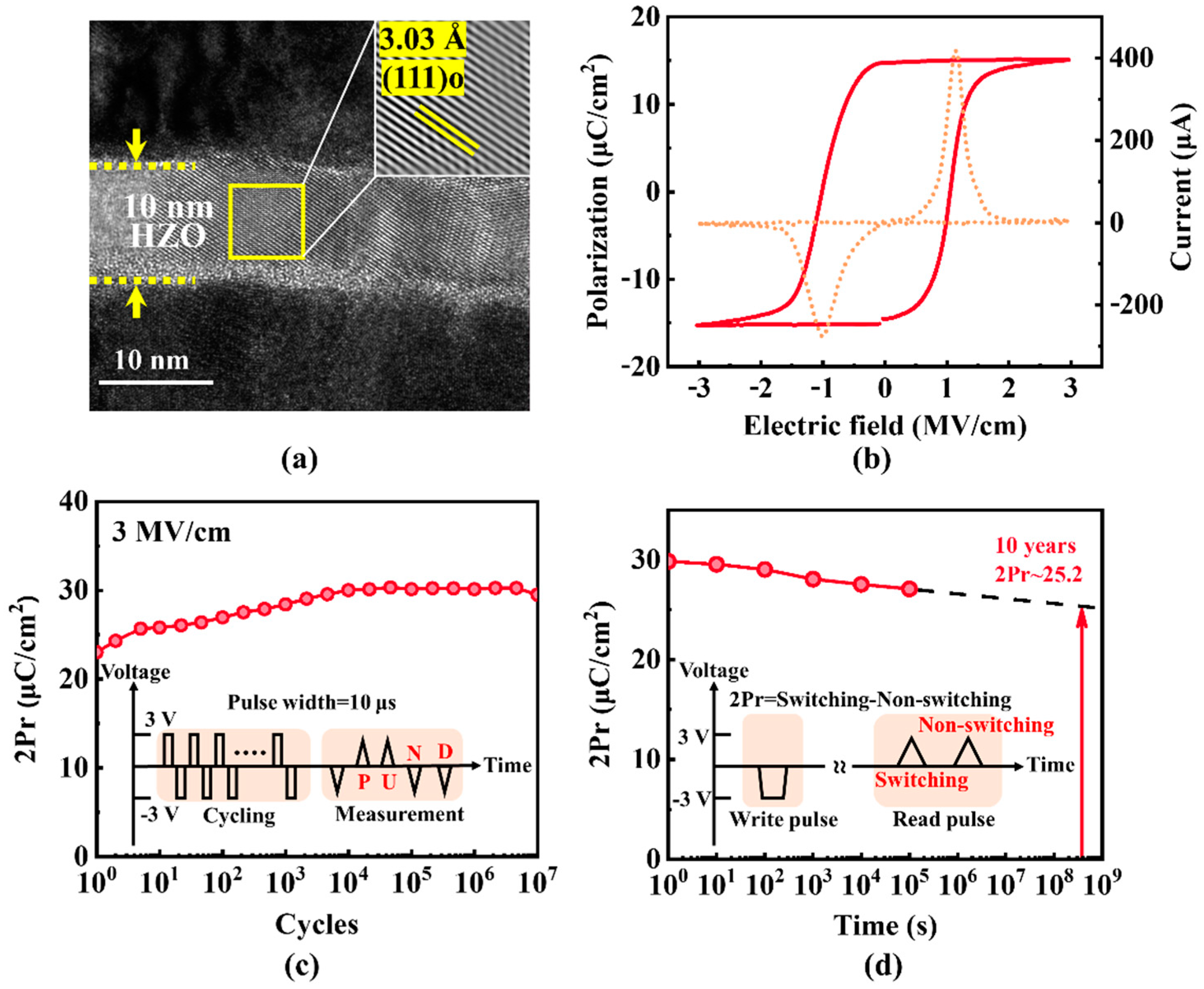
To elucidate the exemplary performance of the 10 nm thick HZO MFM rigid device, a comprehensive analysis of both structural and electrical properties, including remnant polarization, endurance, and retention, is presented in
Figure 2. The cross-sectional HRTEM image in
Figure 2a depicts a smooth and well-defined interface between HZO and W, confirming a film thickness of 10 nm. Additionally, different crystalline structures, including o- and t-phases, are evident in the crystallized HZO film; the interplanar spacing of o(111) is 3.03 Å.
Figure 2b exhibits P-E curves after a wake-up of 10
4 cycles, portraying a ferroelectric P-E loop with large Pr and a minimal coercive field (Ec). Notably, the 2Pr value reaches 30.1 μC/cm
2.
Endurance characterization, as depicted in
Figure 2c, underscores the robust properties of the HZO thin film. Endurance tests, under the same switching conditions as P-E measurements, reveal a stable 2Pr over 10
7 cycles at cycling pulses of ±3 MV/cm without dielectric breakdown. Even at 10
7 cycles, the 2Pr value experiences only a marginal decrease of 1.8% compared to that at 10
4 cycles.
Figure 2d shows data retention, with 2Pr remaining at 27.1 μC/cm
2 for up to 10
5 s, demonstrating slight degradation extended over 10 years. The retention measurement predicts that the 2Pr remains at 25.2 μC/cm
2 after 10 years. These results substantiate the outstanding performance of the rigid ferroelectric device, showing advantages over the existing HZO devices [
21], paving the way for the fabrication of flexible devices.
To assess the crystallinity of the HZO film in both rigid and flexible capacitors, GIXRD measurements at an incidence angle of 0.5° were conducted (
Figure 3a). The measurements were performed at 40 kV voltage and a 40 mA current with a scanning rate of 0.5°/min. Notably, the absence of peaks associated with the m-phase in both capacitors, coupled with the presence of o(111) and t(011) peaks, attested to the preserved crystallinity. In the case of t- and o-phases, the peaks associated with o(111) and t(011) phases were observed at the same angle, as these phases could not be distinguished, owing to their structural similarity. To distinguish between o- and t-phases, a Gaussian peak fitting for devices was performed. Each phase ratio was calculated from the ratio of the integrated peak intensity corresponding to the o- and t-phase in GIXRD patterns. The decrease in the o(111)/t(011) peak was due to the reduction in the t-phase caused by stress during ICP etching [
10]. The o-phase directly affected ferroelectricity in HZO ferroelectric films. We can conclude that the crystalline structure is not affected by etching when the crystalline structure of the o-phase remains unchanged. In other words, the diffraction peaks in both capacitors indicate that ICP etching does not compromise the crystalline structure of the film. Therefore, the electrical properties of the devices were also explored, which more directly indicates the effect of etching on the HZO film.
With a silicon substrate thickness of approximately 50 μm, the device possesses inherent flexibility but is susceptible to fracture due to a limited bending threshold. Introducing a metal buffer layer at the back of the silicon substrate effectively enhances the bending limit. The mechanical advantage of flexible devices with different metal buffer layers are elucidated through stress–strain curves. In
Figure 3b, the stress–strain curves for devices without a buffer layer, with Ni, with W, and with an Al buffer layer are compared. The curves delineate the internal stress and strain distribution under uniform applied load conditions. Notably, the flexible devices exhibit elastic deformation before reaching a certain degree of deformation, after which they fracture instantly. Devices without the buffer layer break at a strain of 0.056, corresponding to a maximum stress of 0.26 MPa. The flexible devices with Ni and W buffer layers break at slightly higher strains of 0.061 and 0.059, with maximum stresses of 0.29 MPa and 0.27 MPa, respectively. Notably, the flexible device with an Al buffer layer showcases significantly improved mechanical properties, particularly in the bending limit, breaking at a strain of 0.084, corresponding to a maximum stress of 0.46 MPa. These findings underscore the pronounced mechanical enhancements conferred by the Al buffer layer, signifying its efficacy in augmenting the flexibility and durability of the flexible device. This outstanding property can be attributed to the small elastic modulus of Al. The elastic modulus of W is 410 GPa and 200 GPa for Ni. Both of the elastic moduli are larger than Si (130–190 GPa). Materials with a large elastic modulus are not prone to deformation, which is unfavorable for flexible devices. However, the elastic modulus of Al is only 70 GPa, improving the bending limit of flexible devices.
The thinning of the Si substrate is accomplished through RIE etching, utilizing ion energy to form a readily etched damage layer on the Si substrate’s surface. The F plasma group produced by the etching gas reacts with Si to generate SiF4 gas. Simultaneously, a 50 nm Al buffer layer is grown through the evaporation process. Al, a common and cost-effective conductive material in semiconductor manufacturing, forms a robust combination with Si. However, the high etching power of ICP, especially in prolonged and high-power processes, may exert irreversible effects on ferroelectricity. Additionally, the ultrathin silicon substrate resulting from RIE etching and the evaporation process can potentially compromise device reliability. Therefore, an exploration of the impact of RIE etching and evaporation on ferroelectricity is imperative through electrical tests.
Figure 3c compares the P-E loop of the rigid device (pre-thinning), the flexible device without the Al buffer layer, and the flexible device with the Al buffer layer. The positive remnant polarization (Pr
+) value is 16.3 μC/cm
2, 15.4 μC/cm
2, and 15.5 μC/cm
2, respectively, while the negative remnant polarization (Pr
−) is −15.5 μC/cm
2, −15.1 μC/cm
2, and −14.1 μC/cm
2, respectively. Similarly, positive coercive electric (Ec
+) and negative coercive electric (Ec
−) values exhibit comparable trends.
Figure 3d illustrates the C-V curves at 100 kHz for these capacitors, revealing typical ferroelectric characteristics with analogous “butterfly” peaks. These results affirm that the critical steps of RIE etching and evaporating do not compromise device performance, establishing their utility in the preparation of flexible devices.
Figure 3d shows the C-V curves at 100 kHz for these three devices, revealing typical ferroelectric characteristics with analogous “butterfly” peaks [
22]. The buffer layer device shows differences from other devices in capacitance change in the positive voltage region, and the decrease in the capacitance value results from the measurement method. Since the resistance of the n-Si substrate is only 0.01 Ω, the voltage is input from the top electrode in C-V measurement, and the substrate is grounded. Additionally, the Al layer of the buffer layer device is grounded in the measurement method. The altered interface affects the response of the polarization charge to the voltage; the capacitance value in the positive voltage region exhibits differences. But the curve exhibits the typical ferroelectric characteristics with analogous “butterfly” peaks. Therefore, the results affirm that the critical steps of etching and evaporating do not compromise device performance, establishing their utility in the preparation of flexible devices.
To investigate the electrical performance of the flexible devices under various bending states, biases of ±3V were applied to the top electrode using the PUND measurement. Flexible devices, fixed on the molds with distinct bending radii, were subjected to a different outward bending radius (18 mm, 15 mm, 12 mm, 8 mm, and 5 mm).
Figure 4a illustrates the variation in 2Pr (without a buffer layer) from 29.2 μC/cm
2 to 28.3 μC/cm
2 as the outward bending radius decreases from 18 mm to 5 mm. Conversely, the flexible device with the Al buffer layer maintains a consistent 2Pr at 29.5± 0.5 μC/cm
2 despite changes in the bending radius from 18 mm to 5 mm, which is similar to the flexible HZO devices on organic substrates [
23]. The performance of the device with the Al layer significantly improves under outward bending. To further investigate the flexibility of flexible devices, a series of tests were conducted, subjecting them to an outward bending radius of 12 mm for varying cycles. The variations in 2Pr with increasing outward bending cycles are depicted in
Figure 4b. Irrespective of the presence of the Al buffer layer on the back of the device, both configurations exhibited a decline in 2Pr after 6000 bending cycles, settling at 23.4 μC/cm
2 and 22.1 μC/cm
2, respectively. This observed ferroelectric degradation is likely attributable to the continuous bending, which induced changes in the crystalline structure within the film.
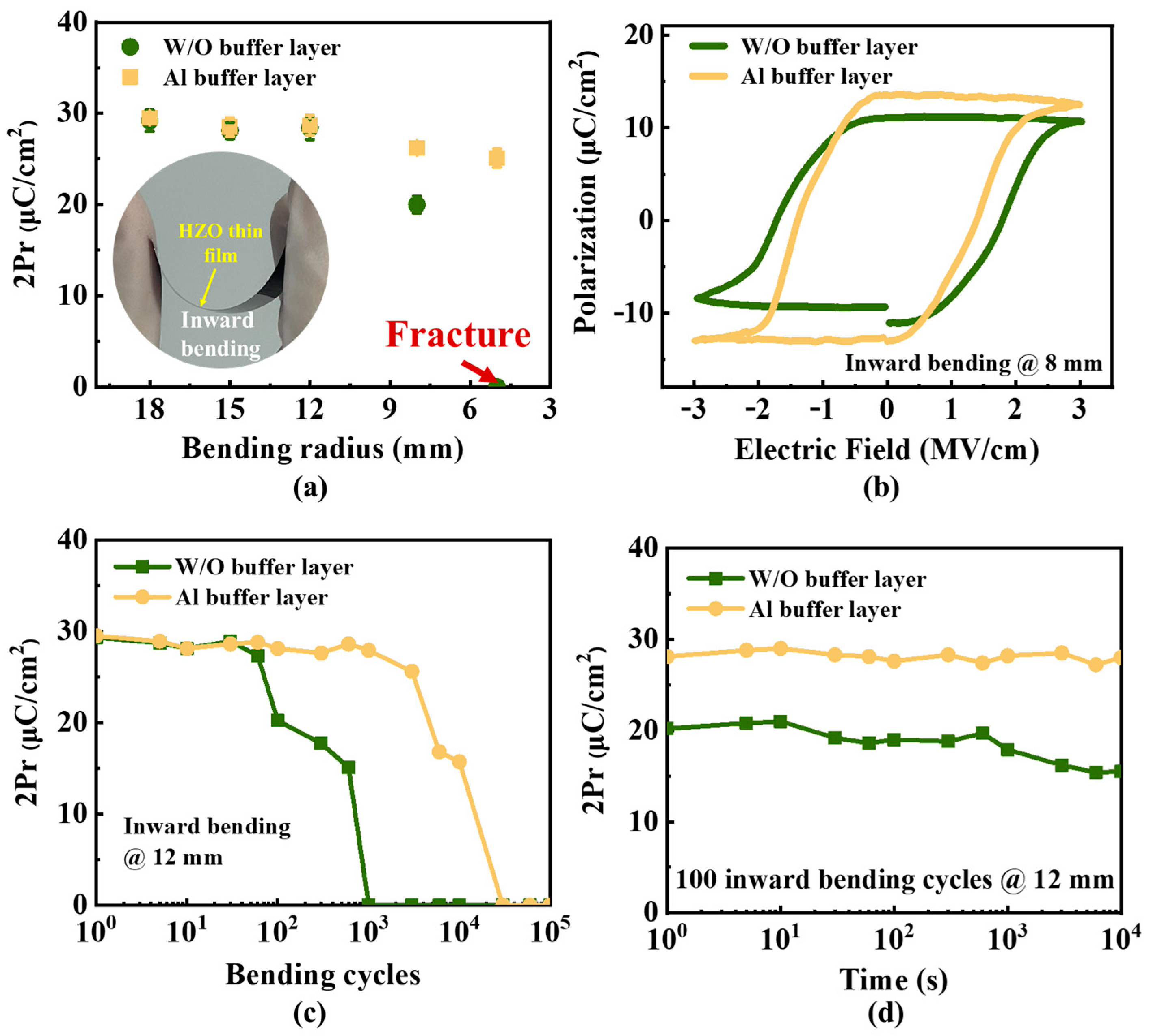
Figure 5a shows the variations in 2Pr as the inward bending radius decreases, subjecting the device to tensile stress on the substrate. For the device without the Al buffer layer, 2Pr remains relatively consistent with the flat state at larger bending radii, recording values of 29.2 μC/cm
2, 28.1 μC/cm
2, and 28.4 μC/cm
2 at 18 mm, 15 mm, and 12 mm inward bending radii, respectively. However, a substantial decrease to 20 μC/cm
2 is observed at an inward bending radius of 8 mm, reflecting a 31% reduction. The device fractures outright when the bending radius is further reduced to 5 mm. Conversely, devices equipped with the Al buffer layer exhibit 2Pr values of 26.2 μC/cm
2 and 25.1 μC/cm
2 at inward bending radii of 8 mm and 5 mm, respectively. This outcome highlights the capacity of the Al buffer layer to enhance the bending limit, allowing the capacitor to maintain stable ferroelectric properties even at small inward bending radii.
Figure 5b presents the P-E loops for devices with and without the Al buffer layer at an inward bending radius of 8 mm. The device without the buffer layer exhibits Pr
+ of 11.1 μC/cm
2, Pr
− of −9.3 μC/cm
2, Ec
+ of 1.8 MV/cm, and Ec
− of −1.7 MV/cm. In comparison, the device with the Al buffer layer demonstrates superior ferroelectric characteristics, featuring Pr
+ of 13.5 μC/cm
2, Pr
− of −12.7 μC/cm
2, Ec
+ of 1.4 MV/cm, and Ec
− of −1.4 MV/cm.
The evolution of 2Pr with increasing inward bending cycles is presented in
Figure 5c. The device without the Al buffer layer experiences a decrease to 20.2 μC/cm
2 after 100 bending cycles at a 12 mm inward radius, ultimately leading to fracture after 1000 bending cycles. By contrast, the device with the Al buffer layer exhibits a decrease to 16.8 μC/cm
2 after 6000 bending cycles, with brittle breaking observed after 30,000 bending cycles. This underscores the substantial improvement in the bending limit and stress resistance conferred by the Al buffer layer. Finally,
Figure 5d depicts the retention performance after 100 cycles at an inward bending radius of 12 mm, revealing that the capacitor with the Al layer maintains 2Pr at 28.1 μC/cm
2 up to 10
4 s, demonstrating stable polarization retention.
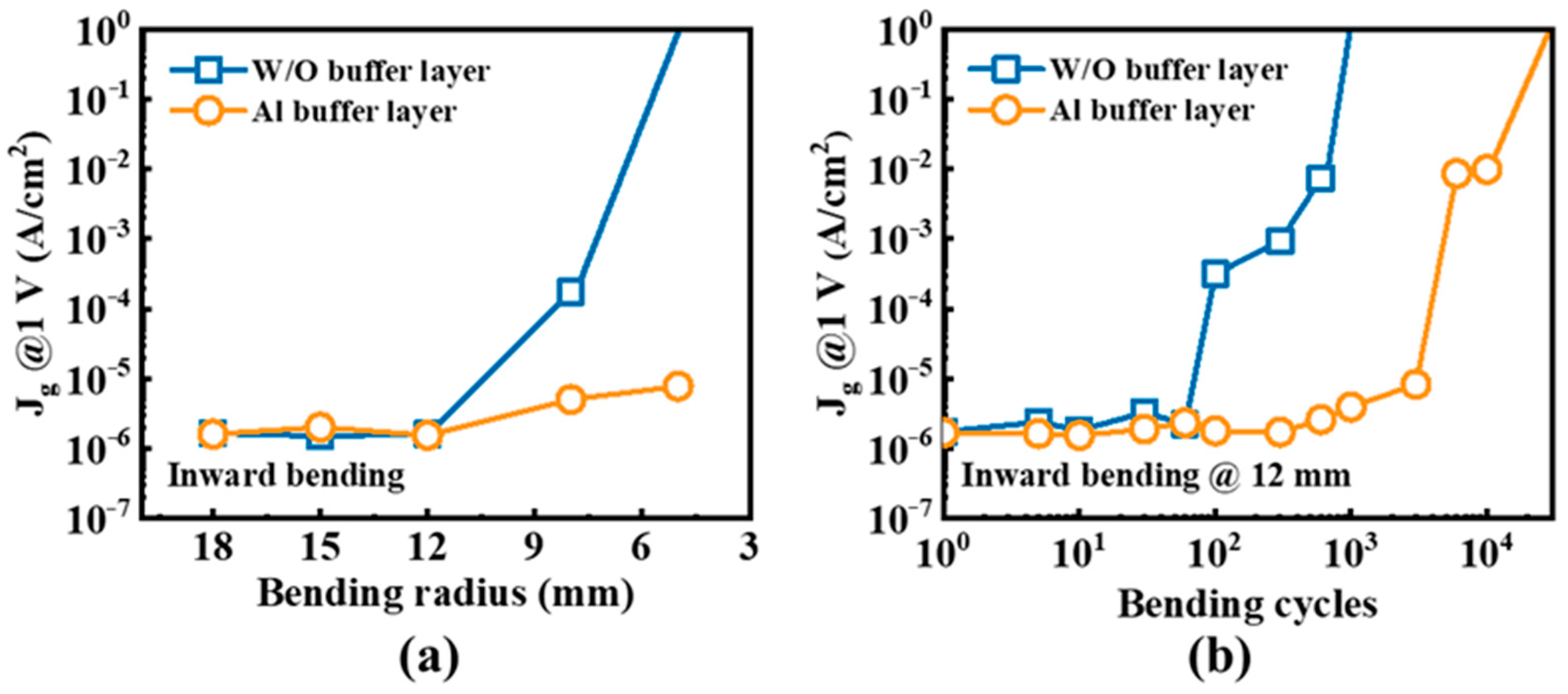
Ferroelectric films, theoretically belonging to insulating materials with high dielectric constants, may exhibit substantial leakage current due to inherent defects. The analysis involves applying a voltage with a specified step and recording the corresponding current values. In
Figure 6a, the variation in leakage current density with an inward bending radius is depicted. For the device without the Al buffer layer, the leakage current (at 1 V) stands at 1.6 × 10
−6 A/cm
2, 1.5 × 10
−6 A/cm
2, 1.6 × 10
−6 A/cm
2, 1.7 × 10
−4 A/cm
2, and 0 A/cm
2 at inward bending radii of 18 mm, 15 mm, 12 mm, 8 mm, and 5 mm, respectively. The flexible device with the Al buffer shows successive leakage current values of 1.6 × 10
−6 A/cm
2, 2.0 × 10
−6 A/cm
2, 1.5 × 10
−6 A/cm
2, 5.0 × 10
−6 A/cm
2, and 7.8 × 10
−6 A/cm
2 at the corresponding bending radii. Correlating with the trends observed in 2Pr (
Figure 5a), the substantial leakage current in HZO thin films indicates degradation in remanent polarization.
Figure 6b illustrates the relationship between leakage current density and inward bending cycles. For the device without the Al buffer layer, the leakage current density reaches 3.2 × 10
−4 A/cm
2 after 100 bending cycles. By contrast, the flexible device with the Al buffer layer exhibits an increased leakage current of 8.7 × 10
−4 A/cm
2 after 6000 bending cycles. The stress induced during bending contributes to damage within the HZO ferroelectric film, a phenomenon that the Al buffer layer helps mitigate. It is hypothesized that the heightened leakage current may stem from the formation cracks in the HZO ferroelectric film during bending [
24].
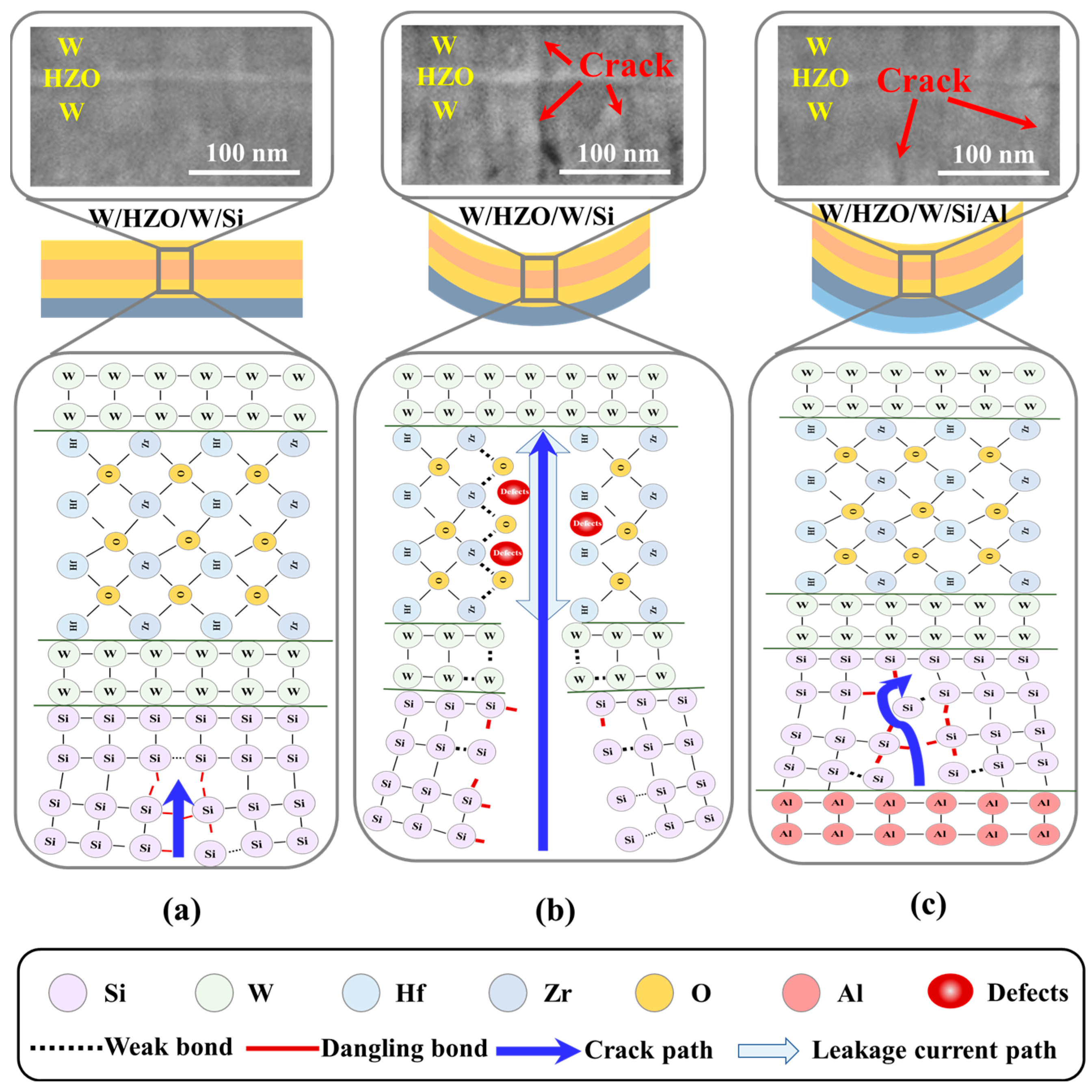
The results indicate a decline in ferroelectricity for the flexible device without the Al buffer layer at the inward bending radius of 8 mm, with 2Pr diminishing to 20.2 μC/cm
2 after 100 inward bending cycles. This degradation is attributed to crack formation within the ferroelectric thin film, primarily stemming from the expansion of the Si substrate toward the film’s interior. To investigate further, focused ion beam (FIB) cutting was employed on both the unbent flexible device and the one without the buffer layer after 100 inward bending cycles. The subsequent scanning electron microscope (SEM) analysis of the W/HZO/W section is illustrated in
Figure 7a,b.
In the absence of bending stress, the W/HZO/W section appears relatively flat with minimal visible cracks (
Figure 7a). However, for the flexible device without the buffer layer after 100 inward bending cycles, numerous cracks are evident, perpendicular to the HZO film. Notably, the cracks in the bottom electrode area are denser, reaching a size of 20 nm. These observations suggest that cracks penetrating the HZO film from the bottom electrode to the top electrode induce damage to the internal crystalline structure and chemical bond of HZO, leading to ferroelectricity degradation and an increase in leakage current. The high-power RIE etching process is acknowledged to introduce defects, and, when the flexible device undergoes inward bending, the tensile load applied to the substrate results in extensive crack formation at these defects. As the bending radius decreases or bending cycles increase, stress-induced cracks expand from the substrate to the ferroelectric film, as shown in
Figure 7b. These cracks emerge as primary contributors to ferroelectric degradation in HZO thin films. Thus, impeding crack growth into HZO through alternative methods can effectively enhance the bending limit and preserve ferroelectric properties.
The incorporation of the Al buffer layer on the back of the flexible device proves highly effective in improving the bending limit. Even at an inward radius of 8 mm, the 2Pr remains at 25.1 μC/cm
2, experiencing only a modest decrease to 16.8 μC/cm
2 after 6000 inward bending cycles. The performance improvement can be attributed to the inhibition of the crack growth by the Al layer. To validate this inhibitory effect, FIB cutting is performed on the device after 100 inward bending cycles, and SEM analysis of the W/HZO/W section is presented in
Figure 7c. The section with the Al buffer layer exhibits only a few cracks at the interface between the bottom electrode and the Si substrate, resembling the section of the unbent device. This observation supports the conclusion that the Al buffer layer effectively suppresses crack growth, thereby preventing the destruction of ferroelectric film.
Mechanical properties offer insight into the effectiveness of the Al buffer layer. With an elastic modulus 70 GPa for Al and the 130–190 GPa for Si, differences in their ability to resist bending deformation are present [
25,
26]. The Al buffer layer and the Si substrate undergo different degrees of deformation during inward bending, generating internal forces to resist the bending stress and maintain balance (referred to as additional stress). This additional stress generated by the dense Al buffer layer is transmitted to the Si substrate, which reduces the bending-induced stress on the Si substrate. Consequently, the diminished bending stress leads to a reduced crack growth, and, in some cases, the suppression of crack growth. The positions of the two ends of the crack, with one end at the interface between the Al buffer layer and the Si substrate and other end located inside the Si substrate, further contribute to the non-equilibrium state of Al buffer layer and the substrate during inward bending. This mismatch in elastic modulus affects the path of crack growth, as illustrated in
Figure 7c.
